EP4492469A1 - Verfahren zur herstellung einer lichtemittierenden vorrichtung - Google Patents
Verfahren zur herstellung einer lichtemittierenden vorrichtung Download PDFInfo
- Publication number
- EP4492469A1 EP4492469A1 EP24184462.0A EP24184462A EP4492469A1 EP 4492469 A1 EP4492469 A1 EP 4492469A1 EP 24184462 A EP24184462 A EP 24184462A EP 4492469 A1 EP4492469 A1 EP 4492469A1
- Authority
- EP
- European Patent Office
- Prior art keywords
- dielectric layer
- pixels
- layer
- etching
- substrate
- Prior art date
- Legal status (The legal status is an assumption and is not a legal conclusion. Google has not performed a legal analysis and makes no representation as to the accuracy of the status listed.)
- Granted
Links
Images




Classifications
-
- H—ELECTRICITY
- H10—SEMICONDUCTOR DEVICES; ELECTRIC SOLID-STATE DEVICES NOT OTHERWISE PROVIDED FOR
- H10H—INORGANIC LIGHT-EMITTING SEMICONDUCTOR DEVICES HAVING POTENTIAL BARRIERS
- H10H20/00—Individual inorganic light-emitting semiconductor devices having potential barriers, e.g. light-emitting diodes [LED]
- H10H20/01—Manufacture or treatment
- H10H20/011—Manufacture or treatment of bodies, e.g. forming semiconductor layers
- H10H20/013—Manufacture or treatment of bodies, e.g. forming semiconductor layers having light-emitting regions comprising only Group III-V materials
- H10H20/0133—Manufacture or treatment of bodies, e.g. forming semiconductor layers having light-emitting regions comprising only Group III-V materials with a substrate not being Group III-V materials
- H10H20/01335—Manufacture or treatment of bodies, e.g. forming semiconductor layers having light-emitting regions comprising only Group III-V materials with a substrate not being Group III-V materials the light-emitting regions comprising nitride materials
-
- H—ELECTRICITY
- H10—SEMICONDUCTOR DEVICES; ELECTRIC SOLID-STATE DEVICES NOT OTHERWISE PROVIDED FOR
- H10H—INORGANIC LIGHT-EMITTING SEMICONDUCTOR DEVICES HAVING POTENTIAL BARRIERS
- H10H20/00—Individual inorganic light-emitting semiconductor devices having potential barriers, e.g. light-emitting diodes [LED]
- H10H20/80—Constructional details
- H10H20/81—Bodies
- H10H20/811—Bodies having quantum effect structures or superlattices, e.g. tunnel junctions
- H10H20/812—Bodies having quantum effect structures or superlattices, e.g. tunnel junctions within the light-emitting regions, e.g. having quantum confinement structures
-
- H—ELECTRICITY
- H10—SEMICONDUCTOR DEVICES; ELECTRIC SOLID-STATE DEVICES NOT OTHERWISE PROVIDED FOR
- H10H—INORGANIC LIGHT-EMITTING SEMICONDUCTOR DEVICES HAVING POTENTIAL BARRIERS
- H10H20/00—Individual inorganic light-emitting semiconductor devices having potential barriers, e.g. light-emitting diodes [LED]
- H10H20/80—Constructional details
- H10H20/81—Bodies
- H10H20/813—Bodies having a plurality of light-emitting regions, e.g. multi-junction LEDs or light-emitting devices having photoluminescent regions within the bodies
-
- H—ELECTRICITY
- H10—SEMICONDUCTOR DEVICES; ELECTRIC SOLID-STATE DEVICES NOT OTHERWISE PROVIDED FOR
- H10H—INORGANIC LIGHT-EMITTING SEMICONDUCTOR DEVICES HAVING POTENTIAL BARRIERS
- H10H20/00—Individual inorganic light-emitting semiconductor devices having potential barriers, e.g. light-emitting diodes [LED]
- H10H20/80—Constructional details
- H10H20/81—Bodies
- H10H20/819—Bodies characterised by their shape, e.g. curved or truncated substrates
-
- H—ELECTRICITY
- H10—SEMICONDUCTOR DEVICES; ELECTRIC SOLID-STATE DEVICES NOT OTHERWISE PROVIDED FOR
- H10H—INORGANIC LIGHT-EMITTING SEMICONDUCTOR DEVICES HAVING POTENTIAL BARRIERS
- H10H20/00—Individual inorganic light-emitting semiconductor devices having potential barriers, e.g. light-emitting diodes [LED]
- H10H20/80—Constructional details
- H10H20/81—Bodies
- H10H20/819—Bodies characterised by their shape, e.g. curved or truncated substrates
- H10H20/821—Bodies characterised by their shape, e.g. curved or truncated substrates of the light-emitting regions, e.g. non-planar junctions
-
- H—ELECTRICITY
- H10—SEMICONDUCTOR DEVICES; ELECTRIC SOLID-STATE DEVICES NOT OTHERWISE PROVIDED FOR
- H10H—INORGANIC LIGHT-EMITTING SEMICONDUCTOR DEVICES HAVING POTENTIAL BARRIERS
- H10H20/00—Individual inorganic light-emitting semiconductor devices having potential barriers, e.g. light-emitting diodes [LED]
- H10H20/80—Constructional details
- H10H20/81—Bodies
- H10H20/822—Materials of the light-emitting regions
- H10H20/824—Materials of the light-emitting regions comprising only Group III-V materials, e.g. GaP
- H10H20/825—Materials of the light-emitting regions comprising only Group III-V materials, e.g. GaP containing nitrogen, e.g. GaN
-
- H—ELECTRICITY
- H10—SEMICONDUCTOR DEVICES; ELECTRIC SOLID-STATE DEVICES NOT OTHERWISE PROVIDED FOR
- H10H—INORGANIC LIGHT-EMITTING SEMICONDUCTOR DEVICES HAVING POTENTIAL BARRIERS
- H10H20/00—Individual inorganic light-emitting semiconductor devices having potential barriers, e.g. light-emitting diodes [LED]
- H10H20/80—Constructional details
- H10H20/84—Coatings, e.g. passivation layers or antireflective coatings
-
- H—ELECTRICITY
- H10—SEMICONDUCTOR DEVICES; ELECTRIC SOLID-STATE DEVICES NOT OTHERWISE PROVIDED FOR
- H10H—INORGANIC LIGHT-EMITTING SEMICONDUCTOR DEVICES HAVING POTENTIAL BARRIERS
- H10H29/00—Integrated devices, or assemblies of multiple devices, comprising at least one light-emitting semiconductor element covered by group H10H20/00
- H10H29/01—Manufacture or treatment
- H10H29/011—Manufacture or treatment of integrated devices comprising at least one light-emitting semiconductor component covered by group H10H20/00
-
- H—ELECTRICITY
- H10—SEMICONDUCTOR DEVICES; ELECTRIC SOLID-STATE DEVICES NOT OTHERWISE PROVIDED FOR
- H10H—INORGANIC LIGHT-EMITTING SEMICONDUCTOR DEVICES HAVING POTENTIAL BARRIERS
- H10H29/00—Integrated devices, or assemblies of multiple devices, comprising at least one light-emitting semiconductor element covered by group H10H20/00
- H10H29/01—Manufacture or treatment
- H10H29/034—Manufacture or treatment of coatings
-
- H—ELECTRICITY
- H10—SEMICONDUCTOR DEVICES; ELECTRIC SOLID-STATE DEVICES NOT OTHERWISE PROVIDED FOR
- H10H—INORGANIC LIGHT-EMITTING SEMICONDUCTOR DEVICES HAVING POTENTIAL BARRIERS
- H10H29/00—Integrated devices, or assemblies of multiple devices, comprising at least one light-emitting semiconductor element covered by group H10H20/00
- H10H29/01—Manufacture or treatment
- H10H29/036—Manufacture or treatment of packages
- H10H29/0362—Manufacture or treatment of packages of encapsulations
-
- H—ELECTRICITY
- H10—SEMICONDUCTOR DEVICES; ELECTRIC SOLID-STATE DEVICES NOT OTHERWISE PROVIDED FOR
- H10H—INORGANIC LIGHT-EMITTING SEMICONDUCTOR DEVICES HAVING POTENTIAL BARRIERS
- H10H29/00—Integrated devices, or assemblies of multiple devices, comprising at least one light-emitting semiconductor element covered by group H10H20/00
- H10H29/10—Integrated devices comprising at least one light-emitting semiconductor component covered by group H10H20/00
- H10H29/14—Integrated devices comprising at least one light-emitting semiconductor component covered by group H10H20/00 comprising multiple light-emitting semiconductor components
- H10H29/142—Two-dimensional arrangements, e.g. asymmetric LED layout
-
- H—ELECTRICITY
- H10—SEMICONDUCTOR DEVICES; ELECTRIC SOLID-STATE DEVICES NOT OTHERWISE PROVIDED FOR
- H10H—INORGANIC LIGHT-EMITTING SEMICONDUCTOR DEVICES HAVING POTENTIAL BARRIERS
- H10H29/00—Integrated devices, or assemblies of multiple devices, comprising at least one light-emitting semiconductor element covered by group H10H20/00
- H10H29/80—Constructional details
- H10H29/842—Coatings, e.g. passivation layers or antireflective coatings
-
- H—ELECTRICITY
- H10—SEMICONDUCTOR DEVICES; ELECTRIC SOLID-STATE DEVICES NOT OTHERWISE PROVIDED FOR
- H10H—INORGANIC LIGHT-EMITTING SEMICONDUCTOR DEVICES HAVING POTENTIAL BARRIERS
- H10H29/00—Integrated devices, or assemblies of multiple devices, comprising at least one light-emitting semiconductor element covered by group H10H20/00
- H10H29/80—Constructional details
- H10H29/85—Packages
- H10H29/852—Encapsulations
- H10H29/854—Encapsulations characterised by their material, e.g. epoxy or silicone resins
-
- H—ELECTRICITY
- H10—SEMICONDUCTOR DEVICES; ELECTRIC SOLID-STATE DEVICES NOT OTHERWISE PROVIDED FOR
- H10H—INORGANIC LIGHT-EMITTING SEMICONDUCTOR DEVICES HAVING POTENTIAL BARRIERS
- H10H20/00—Individual inorganic light-emitting semiconductor devices having potential barriers, e.g. light-emitting diodes [LED]
- H10H20/01—Manufacture or treatment
- H10H20/034—Manufacture or treatment of coatings
-
- H—ELECTRICITY
- H10—SEMICONDUCTOR DEVICES; ELECTRIC SOLID-STATE DEVICES NOT OTHERWISE PROVIDED FOR
- H10H—INORGANIC LIGHT-EMITTING SEMICONDUCTOR DEVICES HAVING POTENTIAL BARRIERS
- H10H20/00—Individual inorganic light-emitting semiconductor devices having potential barriers, e.g. light-emitting diodes [LED]
- H10H20/80—Constructional details
- H10H20/81—Bodies
- H10H20/813—Bodies having a plurality of light-emitting regions, e.g. multi-junction LEDs or light-emitting devices having photoluminescent regions within the bodies
- H10H20/8132—Laterally arranged light-emitting regions, e.g. nano-rods
-
- H—ELECTRICITY
- H10—SEMICONDUCTOR DEVICES; ELECTRIC SOLID-STATE DEVICES NOT OTHERWISE PROVIDED FOR
- H10H—INORGANIC LIGHT-EMITTING SEMICONDUCTOR DEVICES HAVING POTENTIAL BARRIERS
- H10H20/00—Individual inorganic light-emitting semiconductor devices having potential barriers, e.g. light-emitting diodes [LED]
- H10H20/80—Constructional details
- H10H20/81—Bodies
- H10H20/817—Bodies characterised by the crystal structures or orientations, e.g. polycrystalline, amorphous or porous
- H10H20/818—Bodies characterised by the crystal structures or orientations, e.g. polycrystalline, amorphous or porous within the light-emitting regions
-
- H—ELECTRICITY
- H10—SEMICONDUCTOR DEVICES; ELECTRIC SOLID-STATE DEVICES NOT OTHERWISE PROVIDED FOR
- H10H—INORGANIC LIGHT-EMITTING SEMICONDUCTOR DEVICES HAVING POTENTIAL BARRIERS
- H10H29/00—Integrated devices, or assemblies of multiple devices, comprising at least one light-emitting semiconductor element covered by group H10H20/00
- H10H29/01—Manufacture or treatment
- H10H29/012—Manufacture or treatment of active-matrix LED displays
-
- H—ELECTRICITY
- H10—SEMICONDUCTOR DEVICES; ELECTRIC SOLID-STATE DEVICES NOT OTHERWISE PROVIDED FOR
- H10H—INORGANIC LIGHT-EMITTING SEMICONDUCTOR DEVICES HAVING POTENTIAL BARRIERS
- H10H29/00—Integrated devices, or assemblies of multiple devices, comprising at least one light-emitting semiconductor element covered by group H10H20/00
- H10H29/01—Manufacture or treatment
- H10H29/036—Manufacture or treatment of packages
- H10H29/0361—Manufacture or treatment of packages of wavelength conversion means
-
- H—ELECTRICITY
- H10—SEMICONDUCTOR DEVICES; ELECTRIC SOLID-STATE DEVICES NOT OTHERWISE PROVIDED FOR
- H10H—INORGANIC LIGHT-EMITTING SEMICONDUCTOR DEVICES HAVING POTENTIAL BARRIERS
- H10H29/00—Integrated devices, or assemblies of multiple devices, comprising at least one light-emitting semiconductor element covered by group H10H20/00
- H10H29/80—Constructional details
- H10H29/85—Packages
- H10H29/851—Wavelength conversion means
- H10H29/8511—Wavelength conversion means characterised by their material, e.g. binder
- H10H29/8512—Wavelength conversion materials
-
- H—ELECTRICITY
- H10—SEMICONDUCTOR DEVICES; ELECTRIC SOLID-STATE DEVICES NOT OTHERWISE PROVIDED FOR
- H10H—INORGANIC LIGHT-EMITTING SEMICONDUCTOR DEVICES HAVING POTENTIAL BARRIERS
- H10H29/00—Integrated devices, or assemblies of multiple devices, comprising at least one light-emitting semiconductor element covered by group H10H20/00
- H10H29/80—Constructional details
- H10H29/85—Packages
- H10H29/8517—Colour filters
Definitions
- the invention relates to the technical field of manufacturing electroluminescent devices.
- the invention finds its application in particular in the manufacture of light-emitting diodes based on nanowires, in particular gallium nitride GaN.
- the encapsulation layer can be made of silicon nitride Si 3 N 4 .
- the dielectric layer is generally made of silicon dioxide SiO 2 .
- step B Such a prior art method is not entirely satisfactory since the strong bombardment of ionized gas in step B) is likely to cause significant degradation of the pixels. This degradation is all the more marked as the form factor (ratio between the height and the width of the pixels) of the pixels is high. It has been observed experimentally that the upper part of the pixels can become beveled at the end of step B).
- step B) is conventionally performed with a fluorinated plasma, such as a carbon tetrafluoride CF 4 plasma.
- a fluorinated plasma such as a carbon tetrafluoride CF 4 plasma.
- the etching depth depends strongly on the carbon/fluorine ratio of the plasma.
- a variation in the relative surface area of the carbon mask can cause an etching stop (“ etch stop ” in English), this undesirable phenomenon being all the more marked as the thickness of the dielectric layer to be etched is significant.
- step b) makes it possible to better protect the columnar pixels compared to the state of the art, thanks to steps b) and c).
- the directional etching (e.g. plasma) carried out during step b) only concerns inter-pixel areas.
- the upper part of the pixels is preserved from a possible strong ionized bombardment, because the part of the dielectric layer overhanging the upper part of the pixels is not etched during step b).
- the selective chemical etching carried out during step c) makes it possible to etch the remaining part of the dielectric layer without significantly affecting the upper part of the pixels, unlike an ionized gas bombardment.
- step c) makes it possible to overcome the etching stoppage problems of the state of the art, linked to plasma etching, when the dielectric layer has a high thickness (e.g. 8 ⁇ m to 10 ⁇ m).
- the method according to the invention may comprise one or more of the following characteristics.
- the method comprises a step d) of forming at least one colored resin on the encapsulation layer at the end of step c), said at least one colored resin being suitable for filtering an emission spectrum of an underlying pixel.
- an advantage provided is to protect the upper part of the pixels during step b).
- the part of the dielectric layer overhanging the upper part of the pixels is not etched during step b), thanks to the photolithography mask having patterns arranged to face the pixels of the pixel matrices.
- one advantage of a trench formed between two adjacent pixel arrays is to limit crosstalk effects.
- the barrier layer allows for better control over the extent of selective (isotropic) chemical etching performed in step c).
- the chemical etching agent with which step c) is carried out is hydrofluoric acid HF in the vapor phase.
- hydrofluoric acid HF in vapor phase is to be compatible, in terms of etching selectivity, with several materials including aluminum Al, alumina Al 2 O 3 , aluminum nitride AlN, which allows a greater choice than wet etching for the materials of the barrier layer and the encapsulation layer.
- the barrier layer deposited during step b02 ) is made of at least one material chosen from aluminum Al, alumina Al2O3 , aluminum nitride AlN.
- step b) is preceded by a step b03 ) of filling the tungsten trench W at the end of step b02 ).
- one advantage provided is to reinforce the mechanical strength of the trenches.
- step b) is preceded by an initial directional etching, following the normal to the surface of the substrate, of a superficial part of the dielectric layer so as to reach a position of the stack located above the pixels of the pixel matrices, at a distance from the encapsulation layer.
- an advantage provided is to limit the operation time of the selective chemical etching carried out during step c), the superficial part of the dielectric layer being already etched beforehand.
- the position reached at the end of the initial directional etching e.g. plasma etching
- the encapsulation layer of the stack used during step a) is made of at least one material chosen from aluminum Al, alumina Al 2 O 3 , aluminum nitride AlN.
- the dielectric layer of the stack used during step a) is made of silicon dioxide SiO 2 .
- the substrate 1 is advantageously made of a semiconductor material.
- the substrate 1 can be made of silicon Si.
- the pixels 2 may be nanowires, in particular made of gallium nitride GaN.
- the pixels 2 advantageously form periodic patterns.
- the encapsulation layer 3 of the stack used during step a) is advantageously made of at least one material chosen from aluminum Al, alumina Al 2 O 3 , aluminum nitride AlN.
- at least one material it is meant that the encapsulation layer 3 can be made of a multilayer material comprising at least one material chosen from aluminum Al, alumina Al 2 O 3 , aluminum nitride AlN.
- the encapsulation layer 3 of the stack used during step a) can have a thickness of the order of 1 ⁇ m.
- the dielectric layer 4 of the stack used during step a) is advantageously made of silicon dioxide SiO 2 .
- the dielectric layer 4 of the stack used during step a) may have a thickness of between 8 ⁇ m and 10 ⁇ m.
- the directional etching carried out during step b) is a directional etching, following the normal to the surface 10 of the substrate 1, of a part of the dielectric layer 4 extending between the pixels 2 of the pixel matrices 2.
- the directional etching carried out during step b) is a dry plasma etching.
- step b) can be carried out with a fluorinated plasma, such as a carbon tetrafluoride CF 4 plasma.
- step b) is advantageously carried out with a photolithography mask M1 having patterns arranged to face the pixels 2 of the pixel matrices 2.
- the patterns of the photolithography mask M1 overhang the pixels 2 of the pixel matrices 2.
- the dielectric layer 4 has a remaining portion 40 at the end of step b).
- the remaining portion 40 of the dielectric layer 4 extends under the patterns of the photolithography mask M1.
- step b 01 can be performed by dry plasma etching.
- step b 01 can include etching by a C 4 F 8 plasma.
- step b 01 ) can include etching of the encapsulation layer 3, for example by a chlorine plasma (eg Cl 2 or BCl 3 ) when the encapsulation layer 3 is made of aluminum Al or alumina Al 2 O 3 .
- Step b 01 ) is advantageously performed by directional etching along the normal to the surface 10 of the substrate 1.
- Step b 02 is performed by a deposition technique allowing the barrier layer 6 to follow the surface topology of the stack. It is not strictly necessary for the deposition technique to produce a conformal deposit (conformity rate equal to 100%). In other words, the deposition technique is chosen to have a conformity rate (ratio between the width of the sides of the deposited barrier layer 6 and the surface thickness of the deposited barrier layer 6) allowing the surface topology of the stack to be followed.
- the barrier layer 6 may be formed during step b 02 ) by chemical vapor deposition or by atomic layer deposition (ALD), these deposition techniques having a good conformity rate.
- the barrier layer 6 deposited during step b 02 ) is advantageously made of at least one material chosen from aluminum Al, alumina Al 2 O 3 , aluminum nitride AlN.
- at least one material it is meant that the barrier layer 6 can be made of a multilayer material comprising at least one material chosen from aluminum Al, alumina Al 2 O 3 , aluminum nitride AlN.
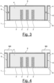
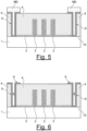
- a portion of the barrier layer 6 (extending between the trenches 5) is etched using a photolithography mask M0 (as illustrated in figures 4 And 5 ) whose patterns cover the trenches 5.
- the photolithography mask M0 can be a photosensitive resin which is then removed from the stack by a removal technique (“ stripping ” in English), as illustrated in figure 6 .
- step b) is advantageously preceded by a step b03 ) of filling the trench 5 with a material 52 of the tungsten W type at the end of step b02 ).
- Step b03 ) is advantageously followed by a step of mechanical-chemical polishing so that the material 52 of the tungsten W type is flush with the stack.
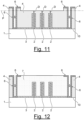
- Step b) is advantageously preceded by an initial directional etching, following the normal to the surface 10 of the substrate 1, of a superficial part of the dielectric layer 4 so as to reach a position P of the stack located above the pixels 2 of the pixel matrices 2, at a distance D from the encapsulation layer 3.
- the position P reached at the end of the initial directional etching eg dry plasma etching
- the distance D can be of the order of a hundred nanometers. More precisely, it is possible to consider a distance D greater than or equal to 100 nm with an etching uniformity of the order of 3%.
- the selective chemical etching performed in step c) is a selective chemical etching of the remaining portion 40 of the dielectric layer 4.
- the selective chemical etching carried out during step c) is an isotropic etching, but may not be total in the sense that certain portions 400 of the remaining part 40 of the dielectric layer 4 (in particular at the ends of the pixel matrices 2) may remain at the end of step c).
- the selective chemical etching carried out during step c) may be total or almost total in the sense that all or almost all of the remaining part 40 of the dielectric layer 4 is removed at the end of step c).
- Step c) is carried out with a chemical etching agent allowing selective etching of the remaining part 40 of the dielectric layer 4 relative to the encapsulation layer 3.
- the chemical etching agent with which step c) is carried out is advantageously hydrofluoric acid HF in the vapor phase.
- step c) is advantageously preceded by a step c0 ) of removing the photolithography mask M1 with which step b) can be carried out.
- the photolithography mask M1 can be a photosensitive resin which is removed from the stack during step c0 ) by a removal technique (“ stripping ” in English).
- the method advantageously comprises a step d) of forming at least one colored resin 7 on the encapsulation layer 3 at the end of step c).
- Said at least one colored resin 7 is suitable for filtering an emission spectrum of an underlying pixel 2.
- Said at least one colored resin 7 may be a resin of the polymer matrix type with quantum dot .
- Said at least one colored resin 7 may be a resin with pigments that can act as a colored filter.
Landscapes
- Electroluminescent Light Sources (AREA)
Applications Claiming Priority (1)
| Application Number | Priority Date | Filing Date | Title |
|---|---|---|---|
| FR2307326A FR3150905B1 (fr) | 2023-07-09 | 2023-07-09 | Procédé de fabrication d’un dispositif électroluminescent |
Publications (2)
| Publication Number | Publication Date |
|---|---|
| EP4492469A1 true EP4492469A1 (de) | 2025-01-15 |
| EP4492469B1 EP4492469B1 (de) | 2025-12-03 |
Family
ID=88413439
Family Applications (1)
| Application Number | Title | Priority Date | Filing Date |
|---|---|---|---|
| EP24184462.0A Active EP4492469B1 (de) | 2023-07-09 | 2024-06-25 | Verfahren zur herstellung einer lichtemittierenden vorrichtung |
Country Status (3)
| Country | Link |
|---|---|
| US (1) | US12272762B2 (de) |
| EP (1) | EP4492469B1 (de) |
| FR (1) | FR3150905B1 (de) |
Citations (2)
| Publication number | Priority date | Publication date | Assignee | Title |
|---|---|---|---|---|
| US20190333963A1 (en) * | 2016-12-29 | 2019-10-31 | Aledia | Optoelectronic device with light-emitting diodes |
| WO2022043053A1 (fr) * | 2020-08-31 | 2022-03-03 | Aledia | Procédé de fabrication d'un dispositif optoélectronique |
Family Cites Families (1)
| Publication number | Priority date | Publication date | Assignee | Title |
|---|---|---|---|---|
| US10553767B2 (en) * | 2017-01-09 | 2020-02-04 | Glo Ab | Light emitting diodes with integrated reflector for a direct view display and method of making thereof |
-
2023
- 2023-07-09 FR FR2307326A patent/FR3150905B1/fr active Active
-
2024
- 2024-06-25 EP EP24184462.0A patent/EP4492469B1/de active Active
- 2024-07-08 US US18/766,529 patent/US12272762B2/en active Active
Patent Citations (2)
| Publication number | Priority date | Publication date | Assignee | Title |
|---|---|---|---|---|
| US20190333963A1 (en) * | 2016-12-29 | 2019-10-31 | Aledia | Optoelectronic device with light-emitting diodes |
| WO2022043053A1 (fr) * | 2020-08-31 | 2022-03-03 | Aledia | Procédé de fabrication d'un dispositif optoélectronique |
Also Published As
| Publication number | Publication date |
|---|---|
| US20250015224A1 (en) | 2025-01-09 |
| EP4492469B1 (de) | 2025-12-03 |
| FR3150905A1 (fr) | 2025-01-10 |
| US12272762B2 (en) | 2025-04-08 |
| FR3150905B1 (fr) | 2025-05-23 |
Similar Documents
| Publication | Publication Date | Title |
|---|---|---|
| EP3826068B1 (de) | Verfahren zum erzeugen einer gemeinsamen elektrode für eine vielzahl von optoelektronischen vorrichtungen | |
| FR2992473A1 (fr) | Procede de fabrication de structures de led ou de cellules solaires | |
| WO2016202899A1 (fr) | Procédé permettant d'obtenir sur un substrat cristallin une couche semi-polaire de nitrure obtenu avec l'un au moins parmi les matériaux suivants :gallium (ga), indium (in) et aluminium (al) | |
| EP3384521B1 (de) | Verfahren zur herstellung einer halbpolaren nitridschicht auf einem kristallinen substrat | |
| EP3987574A1 (de) | Verfahren zur herstellung von nitrid-kacheln zur herstellung einer elektronischen oder optoelektronischen vorrichtung | |
| EP4492469B1 (de) | Verfahren zur herstellung einer lichtemittierenden vorrichtung | |
| EP4539101B1 (de) | Verfahren zur herstellung einer zusammenhängenden nitridschicht | |
| EP3836235B1 (de) | Verfahren zum aufbringen einer strukturierten materialschicht | |
| EP2339616A1 (de) | Hybridsubstrat mit verbesserter Isolierung, und vereinfachtes Herstellungsverfahren eines Hybridsubstrats | |
| EP4020525A1 (de) | Verfahren zur herstellung einer nitridschicht | |
| FR3009430A1 (fr) | Procede de realisation d'un motif dans un circuit integre et circuit integre correspondant | |
| WO2022043053A1 (fr) | Procédé de fabrication d'un dispositif optoélectronique | |
| EP4427260B1 (de) | Oberflächenbehandlungsverfahren | |
| EP4391082B1 (de) | Verfahren zur herstellung einer halbleiteranordnung mit einem rückgitter | |
| EP4248500A1 (de) | Verfahren zur herstellung einer led-vorrichtung | |
| EP3939935B1 (de) | Nanometrisches elektromechanisches stellglied und sein herstellungsverfahren | |
| WO2024126599A1 (fr) | Procédé de préparation d'un empilement en vue d'un collage | |
| EP4730952A1 (de) | Verfahren zur herstellung vertikaler gan-transistoren | |
| FR3150340A1 (fr) | Procédé de formation de motifs ayant des dimensions critiques différentes | |
| WO2025078609A1 (fr) | Dispositif optoélectronique à extraction lumineuse améliorée | |
| EP4299506A1 (de) | Verfahren zur herstellung von konkaven mikrokavitäten | |
| EP4730953A1 (de) | Verfahren zur herstellung vertikaler mikroelektronischer bauelemente auf gan-basis | |
| FR3066316A1 (fr) | Procede de formation d'une structure de planarisation |
Legal Events
| Date | Code | Title | Description |
|---|---|---|---|
| PUAI | Public reference made under article 153(3) epc to a published international application that has entered the european phase |
Free format text: ORIGINAL CODE: 0009012 |
|
| STAA | Information on the status of an ep patent application or granted ep patent |
Free format text: STATUS: REQUEST FOR EXAMINATION WAS MADE |
|
| 17P | Request for examination filed |
Effective date: 20240625 |
|
| AK | Designated contracting states |
Kind code of ref document: A1 Designated state(s): AL AT BE BG CH CY CZ DE DK EE ES FI FR GB GR HR HU IE IS IT LI LT LU LV MC ME MK MT NL NO PL PT RO RS SE SI SK SM TR |
|
| REG | Reference to a national code |
Ipc: H10H0029010000 Ref country code: DE Ref legal event code: R079 Ref document number: 602024001506 Country of ref document: DE Free format text: PREVIOUS MAIN CLASS: H01L0027150000 Ipc: H10H0029010000 |
|
| GRAP | Despatch of communication of intention to grant a patent |
Free format text: ORIGINAL CODE: EPIDOSNIGR1 |
|
| STAA | Information on the status of an ep patent application or granted ep patent |
Free format text: STATUS: GRANT OF PATENT IS INTENDED |
|
| RIC1 | Information provided on ipc code assigned before grant |
Ipc: H10H 29/01 20250101AFI20250718BHEP Ipc: H10H 29/14 20250101ALI20250718BHEP Ipc: H10H 29/80 20250101ALI20250718BHEP Ipc: H10H 29/854 20250101ALI20250718BHEP Ipc: H10H 20/01 20250101ALI20250718BHEP Ipc: H10H 20/819 20250101ALI20250718BHEP Ipc: H10H 29/85 20250101ALN20250718BHEP Ipc: H10H 29/851 20250101ALN20250718BHEP Ipc: H10H 20/813 20250101ALN20250718BHEP Ipc: H10H 20/818 20250101ALN20250718BHEP Ipc: H10H 20/825 20250101ALN20250718BHEP |
|
| INTG | Intention to grant announced |
Effective date: 20250818 |
|
| RIN1 | Information on inventor provided before grant (corrected) |
Inventor name: SOMMER, ROMAIN Inventor name: MEHREZ, ZOUHIR |
|
| GRAS | Grant fee paid |
Free format text: ORIGINAL CODE: EPIDOSNIGR3 |
|
| GRAA | (expected) grant |
Free format text: ORIGINAL CODE: 0009210 |
|
| STAA | Information on the status of an ep patent application or granted ep patent |
Free format text: STATUS: THE PATENT HAS BEEN GRANTED |
|
| AK | Designated contracting states |
Kind code of ref document: B1 Designated state(s): AL AT BE BG CH CY CZ DE DK EE ES FI FR GB GR HR HU IE IS IT LI LT LU LV MC ME MK MT NL NO PL PT RO RS SE SI SK SM TR |
|
| REG | Reference to a national code |
Ref country code: CH Ref legal event code: F10 Free format text: ST27 STATUS EVENT CODE: U-0-0-F10-F00 (AS PROVIDED BY THE NATIONAL OFFICE) Effective date: 20251203 Ref country code: GB Ref legal event code: FG4D Free format text: NOT ENGLISH |
|
| REG | Reference to a national code |
Ref country code: DE Ref legal event code: R096 Ref document number: 602024001506 Country of ref document: DE |
|
| REG | Reference to a national code |
Ref country code: IE Ref legal event code: FG4D Free format text: LANGUAGE OF EP DOCUMENT: FRENCH |
|
| REG | Reference to a national code |
Ref country code: NL Ref legal event code: MP Effective date: 20251203 |
|
| PG25 | Lapsed in a contracting state [announced via postgrant information from national office to epo] |
Ref country code: ES Free format text: LAPSE BECAUSE OF FAILURE TO SUBMIT A TRANSLATION OF THE DESCRIPTION OR TO PAY THE FEE WITHIN THE PRESCRIBED TIME-LIMIT Effective date: 20251203 |
|
| REG | Reference to a national code |
Ref country code: LT Ref legal event code: MG9D |
|
| PG25 | Lapsed in a contracting state [announced via postgrant information from national office to epo] |
Ref country code: NO Free format text: LAPSE BECAUSE OF FAILURE TO SUBMIT A TRANSLATION OF THE DESCRIPTION OR TO PAY THE FEE WITHIN THE PRESCRIBED TIME-LIMIT Effective date: 20260303 |
|
| PG25 | Lapsed in a contracting state [announced via postgrant information from national office to epo] |
Ref country code: FI Free format text: LAPSE BECAUSE OF FAILURE TO SUBMIT A TRANSLATION OF THE DESCRIPTION OR TO PAY THE FEE WITHIN THE PRESCRIBED TIME-LIMIT Effective date: 20251203 Ref country code: HR Free format text: LAPSE BECAUSE OF FAILURE TO SUBMIT A TRANSLATION OF THE DESCRIPTION OR TO PAY THE FEE WITHIN THE PRESCRIBED TIME-LIMIT Effective date: 20251203 |
|
| PG25 | Lapsed in a contracting state [announced via postgrant information from national office to epo] |
Ref country code: RS Free format text: LAPSE BECAUSE OF FAILURE TO SUBMIT A TRANSLATION OF THE DESCRIPTION OR TO PAY THE FEE WITHIN THE PRESCRIBED TIME-LIMIT Effective date: 20260303 |
|
| PG25 | Lapsed in a contracting state [announced via postgrant information from national office to epo] |
Ref country code: PL Free format text: LAPSE BECAUSE OF FAILURE TO SUBMIT A TRANSLATION OF THE DESCRIPTION OR TO PAY THE FEE WITHIN THE PRESCRIBED TIME-LIMIT Effective date: 20251203 |
|
| PG25 | Lapsed in a contracting state [announced via postgrant information from national office to epo] |
Ref country code: LV Free format text: LAPSE BECAUSE OF FAILURE TO SUBMIT A TRANSLATION OF THE DESCRIPTION OR TO PAY THE FEE WITHIN THE PRESCRIBED TIME-LIMIT Effective date: 20251203 |