EP4492658A1 - Dispositifs de gestion d'énergie comprenant de multiples ports d'entrée, et systèmes et procédés associés - Google Patents
Dispositifs de gestion d'énergie comprenant de multiples ports d'entrée, et systèmes et procédés associés Download PDFInfo
- Publication number
- EP4492658A1 EP4492658A1 EP24186671.4A EP24186671A EP4492658A1 EP 4492658 A1 EP4492658 A1 EP 4492658A1 EP 24186671 A EP24186671 A EP 24186671A EP 4492658 A1 EP4492658 A1 EP 4492658A1
- Authority
- EP
- European Patent Office
- Prior art keywords
- capacitor
- energy
- converter
- inductor
- electrically coupled
- Prior art date
- Legal status (The legal status is an assumption and is not a legal conclusion. Google has not performed a legal analysis and makes no representation as to the accuracy of the status listed.)
- Pending
Links
Images








Classifications
-
- H—ELECTRICITY
- H02—GENERATION; CONVERSION OR DISTRIBUTION OF ELECTRIC POWER
- H02J—ELECTRIC POWER NETWORKS; CIRCUIT ARRANGEMENTS OR SYSTEMS FOR SUPPLYING OR DISTRIBUTING ELECTRIC POWER; SYSTEMS FOR STORING ELECTRIC ENERGY
- H02J7/00—Circuit arrangements for charging or discharging batteries or for supplying loads from batteries
- H02J7/34—Parallel operation in networks using both storage and other DC sources, e.g. providing buffering
- H02J7/342—The other DC source being a battery actively interacting with the first one, i.e. battery to battery charging
-
- H—ELECTRICITY
- H02—GENERATION; CONVERSION OR DISTRIBUTION OF ELECTRIC POWER
- H02M—APPARATUS FOR CONVERSION BETWEEN AC AND AC, BETWEEN AC AND DC, OR BETWEEN DC AND DC, AND FOR USE WITH MAINS OR SIMILAR POWER SUPPLY SYSTEMS; CONVERSION OF DC OR AC INPUT POWER INTO SURGE OUTPUT POWER; CONTROL OR REGULATION THEREOF
- H02M1/00—Details of apparatus for conversion
- H02M1/0083—Converters characterised by their input or output configuration
- H02M1/009—Converters characterised by their input or output configuration having two or more independently controlled outputs
-
- H—ELECTRICITY
- H02—GENERATION; CONVERSION OR DISTRIBUTION OF ELECTRIC POWER
- H02J—ELECTRIC POWER NETWORKS; CIRCUIT ARRANGEMENTS OR SYSTEMS FOR SUPPLYING OR DISTRIBUTING ELECTRIC POWER; SYSTEMS FOR STORING ELECTRIC ENERGY
- H02J7/00—Circuit arrangements for charging or discharging batteries or for supplying loads from batteries
- H02J7/80—Circuit arrangements for charging or discharging batteries or for supplying loads from batteries including monitoring or indicating arrangements
- H02J7/82—Control of state of charge [SOC]
-
- H—ELECTRICITY
- H02—GENERATION; CONVERSION OR DISTRIBUTION OF ELECTRIC POWER
- H02M—APPARATUS FOR CONVERSION BETWEEN AC AND AC, BETWEEN AC AND DC, OR BETWEEN DC AND DC, AND FOR USE WITH MAINS OR SIMILAR POWER SUPPLY SYSTEMS; CONVERSION OF DC OR AC INPUT POWER INTO SURGE OUTPUT POWER; CONTROL OR REGULATION THEREOF
- H02M1/00—Details of apparatus for conversion
- H02M1/0095—Hybrid converter topologies, e.g. NPC mixed with flying capacitor, thyristor converter mixed with MMC or charge pump mixed with buck
-
- H—ELECTRICITY
- H02—GENERATION; CONVERSION OR DISTRIBUTION OF ELECTRIC POWER
- H02J—ELECTRIC POWER NETWORKS; CIRCUIT ARRANGEMENTS OR SYSTEMS FOR SUPPLYING OR DISTRIBUTING ELECTRIC POWER; SYSTEMS FOR STORING ELECTRIC ENERGY
- H02J7/00—Circuit arrangements for charging or discharging batteries or for supplying loads from batteries
- H02J7/34—Parallel operation in networks using both storage and other DC sources, e.g. providing buffering
- H02J7/345—Parallel operation in networks using both storage and other DC sources, e.g. providing buffering using capacitors as storage or buffering devices
-
- H—ELECTRICITY
- H02—GENERATION; CONVERSION OR DISTRIBUTION OF ELECTRIC POWER
- H02J—ELECTRIC POWER NETWORKS; CIRCUIT ARRANGEMENTS OR SYSTEMS FOR SUPPLYING OR DISTRIBUTING ELECTRIC POWER; SYSTEMS FOR STORING ELECTRIC ENERGY
- H02J7/00—Circuit arrangements for charging or discharging batteries or for supplying loads from batteries
- H02J7/60—Circuit arrangements for charging or discharging batteries or for supplying loads from batteries including safety or protection arrangements
- H02J7/62—Circuit arrangements for charging or discharging batteries or for supplying loads from batteries including safety or protection arrangements against overcurrent
-
- H—ELECTRICITY
- H02—GENERATION; CONVERSION OR DISTRIBUTION OF ELECTRIC POWER
- H02J—ELECTRIC POWER NETWORKS; CIRCUIT ARRANGEMENTS OR SYSTEMS FOR SUPPLYING OR DISTRIBUTING ELECTRIC POWER; SYSTEMS FOR STORING ELECTRIC ENERGY
- H02J7/00—Circuit arrangements for charging or discharging batteries or for supplying loads from batteries
- H02J7/90—Regulation of charging or discharging current or voltage
- H02J7/96—Regulation of charging or discharging current or voltage in response to battery voltage
-
- H—ELECTRICITY
- H02—GENERATION; CONVERSION OR DISTRIBUTION OF ELECTRIC POWER
- H02M—APPARATUS FOR CONVERSION BETWEEN AC AND AC, BETWEEN AC AND DC, OR BETWEEN DC AND DC, AND FOR USE WITH MAINS OR SIMILAR POWER SUPPLY SYSTEMS; CONVERSION OF DC OR AC INPUT POWER INTO SURGE OUTPUT POWER; CONTROL OR REGULATION THEREOF
- H02M1/00—Details of apparatus for conversion
- H02M1/0003—Details of control, feedback or regulation circuits
- H02M1/0032—Control circuits allowing low power mode operation, e.g. in standby mode
-
- H—ELECTRICITY
- H02—GENERATION; CONVERSION OR DISTRIBUTION OF ELECTRIC POWER
- H02M—APPARATUS FOR CONVERSION BETWEEN AC AND AC, BETWEEN AC AND DC, OR BETWEEN DC AND DC, AND FOR USE WITH MAINS OR SIMILAR POWER SUPPLY SYSTEMS; CONVERSION OF DC OR AC INPUT POWER INTO SURGE OUTPUT POWER; CONTROL OR REGULATION THEREOF
- H02M1/00—Details of apparatus for conversion
- H02M1/0083—Converters characterised by their input or output configuration
-
- H—ELECTRICITY
- H02—GENERATION; CONVERSION OR DISTRIBUTION OF ELECTRIC POWER
- H02M—APPARATUS FOR CONVERSION BETWEEN AC AND AC, BETWEEN AC AND DC, OR BETWEEN DC AND DC, AND FOR USE WITH MAINS OR SIMILAR POWER SUPPLY SYSTEMS; CONVERSION OF DC OR AC INPUT POWER INTO SURGE OUTPUT POWER; CONTROL OR REGULATION THEREOF
- H02M3/00—Conversion of DC power input into DC power output
- H02M3/02—Conversion of DC power input into DC power output without intermediate conversion into AC
- H02M3/04—Conversion of DC power input into DC power output without intermediate conversion into AC by static converters
-
- H—ELECTRICITY
- H02—GENERATION; CONVERSION OR DISTRIBUTION OF ELECTRIC POWER
- H02M—APPARATUS FOR CONVERSION BETWEEN AC AND AC, BETWEEN AC AND DC, OR BETWEEN DC AND DC, AND FOR USE WITH MAINS OR SIMILAR POWER SUPPLY SYSTEMS; CONVERSION OF DC OR AC INPUT POWER INTO SURGE OUTPUT POWER; CONTROL OR REGULATION THEREOF
- H02M3/00—Conversion of DC power input into DC power output
- H02M3/02—Conversion of DC power input into DC power output without intermediate conversion into AC
- H02M3/04—Conversion of DC power input into DC power output without intermediate conversion into AC by static converters
- H02M3/06—Conversion of DC power input into DC power output without intermediate conversion into AC by static converters using resistors or capacitors, e.g. potential divider
- H02M3/07—Conversion of DC power input into DC power output without intermediate conversion into AC by static converters using resistors or capacitors, e.g. potential divider using capacitors charged and discharged alternately by semiconductor devices with control electrode, e.g. charge pumps
-
- H—ELECTRICITY
- H02—GENERATION; CONVERSION OR DISTRIBUTION OF ELECTRIC POWER
- H02M—APPARATUS FOR CONVERSION BETWEEN AC AND AC, BETWEEN AC AND DC, OR BETWEEN DC AND DC, AND FOR USE WITH MAINS OR SIMILAR POWER SUPPLY SYSTEMS; CONVERSION OF DC OR AC INPUT POWER INTO SURGE OUTPUT POWER; CONTROL OR REGULATION THEREOF
- H02M3/00—Conversion of DC power input into DC power output
- H02M3/02—Conversion of DC power input into DC power output without intermediate conversion into AC
- H02M3/04—Conversion of DC power input into DC power output without intermediate conversion into AC by static converters
- H02M3/10—Conversion of DC power input into DC power output without intermediate conversion into AC by static converters using discharge tubes with control electrode or semiconductor devices with control electrode
- H02M3/145—Conversion of DC power input into DC power output without intermediate conversion into AC by static converters using discharge tubes with control electrode or semiconductor devices with control electrode using devices of a triode or transistor type requiring continuous application of a control signal
- H02M3/155—Conversion of DC power input into DC power output without intermediate conversion into AC by static converters using discharge tubes with control electrode or semiconductor devices with control electrode using devices of a triode or transistor type requiring continuous application of a control signal using semiconductor devices only
- H02M3/156—Conversion of DC power input into DC power output without intermediate conversion into AC by static converters using discharge tubes with control electrode or semiconductor devices with control electrode using devices of a triode or transistor type requiring continuous application of a control signal using semiconductor devices only with automatic control of output voltage or current, e.g. switching regulators
- H02M3/158—Conversion of DC power input into DC power output without intermediate conversion into AC by static converters using discharge tubes with control electrode or semiconductor devices with control electrode using devices of a triode or transistor type requiring continuous application of a control signal using semiconductor devices only with automatic control of output voltage or current, e.g. switching regulators including plural semiconductor devices as final control devices for a single load
- H02M3/1582—Buck-boost converters
-
- H—ELECTRICITY
- H02—GENERATION; CONVERSION OR DISTRIBUTION OF ELECTRIC POWER
- H02J—ELECTRIC POWER NETWORKS; CIRCUIT ARRANGEMENTS OR SYSTEMS FOR SUPPLYING OR DISTRIBUTING ELECTRIC POWER; SYSTEMS FOR STORING ELECTRIC ENERGY
- H02J2207/00—Details of circuit arrangements for charging or discharging batteries or supplying loads from batteries
- H02J2207/20—Charging or discharging characterised by the power electronics converter
-
- H—ELECTRICITY
- H02—GENERATION; CONVERSION OR DISTRIBUTION OF ELECTRIC POWER
- H02J—ELECTRIC POWER NETWORKS; CIRCUIT ARRANGEMENTS OR SYSTEMS FOR SUPPLYING OR DISTRIBUTING ELECTRIC POWER; SYSTEMS FOR STORING ELECTRIC ENERGY
- H02J2207/00—Details of circuit arrangements for charging or discharging batteries or supplying loads from batteries
- H02J2207/50—Charging of capacitors, supercapacitors, ultra-capacitors or double layer capacitors
-
- Y—GENERAL TAGGING OF NEW TECHNOLOGICAL DEVELOPMENTS; GENERAL TAGGING OF CROSS-SECTIONAL TECHNOLOGIES SPANNING OVER SEVERAL SECTIONS OF THE IPC; TECHNICAL SUBJECTS COVERED BY FORMER USPC CROSS-REFERENCE ART COLLECTIONS [XRACs] AND DIGESTS
- Y02—TECHNOLOGIES OR APPLICATIONS FOR MITIGATION OR ADAPTATION AGAINST CLIMATE CHANGE
- Y02B—CLIMATE CHANGE MITIGATION TECHNOLOGIES RELATED TO BUILDINGS, e.g. HOUSING, HOUSE APPLIANCES OR RELATED END-USER APPLICATIONS
- Y02B70/00—Technologies for an efficient end-user side electric power management and consumption
- Y02B70/10—Technologies improving the efficiency by using switched-mode power supplies [SMPS], i.e. efficient power electronics conversion e.g. power factor correction or reduction of losses in power supplies or efficient standby modes
Definitions
- Batteries are commonly used to provide power to electronic devices, such as mobile electronic devices. It is frequently desirable that a mobile electronic device have a small form factor. As such, batteries in mobile electronic devices often need to have a small form factor.
- a power management device including multiple input ports includes (a) a first input port configured to be electrically coupled to an energy source, (b) a second input port configured to be electrically coupled to a first capacitor, (c) a first output port configured to be electrically coupled to a first load, and (d) a direct-current-to-direct-current (DC-to-DC) converter configured to (i) charge the first capacitor from energy from the energy source and (ii) provide energy to the first output port at least partially using energy stored in the first capacitor.
- DC-to-DC direct-current-to-direct-current
- a method for powering one or more loads using a power management device includes (a) charging a first capacitor using energy from an energy source, using an inductor of a first direct-current-to-direct-current (DC-to-DC) converter, (b) providing energy to a first load from energy stored in the first capacitor, using the inductor of the first DC-to-DC converter, and (c) transferring energy stored in a second capacitor to the first capacitor, using the inductor of first DC-to-DC converter, the second capacitor being electrically coupled to the first load.
- DC-to-DC direct-current-to-direct-current
- Batteries having a small form factor may be used in size-sensitive applications, such as in wearable electronic device applications and in Internet of Things (IoT) applications.
- Example of batteries that may have a small form factor include, but are not limited to, silver oxide batteries, lithium thionyl chloride batteries, lithium manganese dioxide batteries, and zinc air batteries.
- batteries having a small form factor typically exhibit a high impedance and low specific power, which may be problematic in some applications.
- a wellness wearable electronic device implementing photoplethysmography may have peak loads of 250 milliamperes (mA) or more, and motors in wearable drug delivery pumps may have peak loads in excess of 800 mA.
- IoT Internet of Things
- Nb narrowband radios
- FIGS. 2A and 2B are graphs 200 and 202, respectively, which collectively illustrate one example of operation of battery 100 when subjected to a large peak current load.
- Graph 200 is a graph of current I bat versus time
- graph 202 is a graph of voltage V bat versus time.
- Graphs 200 and 202 have a common time base.
- Current I bat initially has a magnitude of I 1 , but current I bat jumps to a magnitude of I 2 at time t 1 for a short period of time in response to a peak load.
- the spike in current at time t 1 causes voltage V bat to momentarily drop from a magnitude of V 3 to a magnitude of V 1 , and voltage V bat subsequently rebounds to a magnitude of V 3 .
- V 2 the drop in battery voltage V bat at time t 1 will cause voltage supplied to the load to be out of specification, possibly resulting in improper operation of the load. Accordingly, high impedance of a battery in an electronic device may cause improper operation of the electronic device when the battery is subjected to large peak loads. Additionally, certain battery types may be damaged by large peak currents.
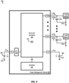
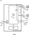
- FIG. 3 is a block diagram of an electrical system 300 including a power management device 302, an energy source 304, a capacitor 306, N loads 308, and N capacitors 310, where N is an integer greater than or equal to one.
- N is an integer greater than or equal to one.
- specific instances of an item may be referred to by use of a numeral in parentheses (e.g. load 308(1)) while numerals without parentheses refer to any such item (e.g. loads 308). While FIG. 3 depicts N being greater than one, it is understood that N could be equal to one.
- Power management device 302, which is one embodiment of the new power management devices disclosed herein, includes a first input port 312, a second input port 314, and N output ports 316.
- First input port 312 is configured to be electrically coupled to energy source 304
- second input port 314 is configured to be electrically coupled to capacitor 306.
- energy source 304 is electrically coupled between first input port 312 and a reference node 318
- capacitor 306 is electrically coupled between second input port 314 and reference node 318.
- Reference node 318 is depicted as being a ground node, such as an earth ground node or a chassis ground node. It is understood, though, that reference node 318 need not be a ground node, and reference node 318 accordingly could be at a different electrical potential than an earth ground or a chassis ground.
- first input port 312, second input port 314, and output ports 316 are discrete elements, such as integrated circuit pins, integrated circuit solder balls or solder tabs, electrical terminals, etc. In some other embodiments, first input port 312, second input port 314, and output ports 316 are respective electrical nodes that optionally encompass a plurality of electrical conductors.
- Energy source 304 could be replaced with a plurality of energy sources electrically coupled in series and/or in parallel, such as to achieve higher energy source capacity than can be practically achieved using a single energy source and/or to achieve a higher energy source voltage than can be practically achieved by using a single energy source. In embodiments including a plurality of energy sources, each energy source need not have the same configuration. Additionally, capacitor 306 could be replaced with a plurality of capacitors electrically coupled in series and/or in parallel, such as to achieve a higher capacitor voltage rating and/or a larger capacitance value than can be practically achieved using a single capacitor. One or more capacitors (not shown) are optionally electrically coupled in parallel with energy source 304.
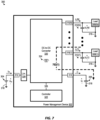
- Controller 322 is configured to cause DC-to-DC converter 320 to operate in one several possible energy transfer modes, such as according to needs electrical system 300. Discussed below with respect to FIGS. 4-8 are several example energy transfer modes of DC-to-DC converter 320 in power management device 302. It is understood, though, that DC-to-DC converter 320 need not be capable of supporting all of the example energy transfer modes. Additionally, DC-to-DC converter 320 could be configured to support alternative and/or additional energy transfer modes without departing from the scope hereof.
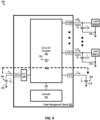
- FIG. 4 is a block diagram of electrical system 300 illustrating an example of controller 322 causing DC-to-DC converter 320 to operate in an input energy transfer mode 402, with an energy transfer path symbolically shown in FIG. 4 by heavy dashed lines, where DC-to-DC converter 320 transfers energy from first input port 312 to second input port 314. Consequently, capacitor 306 is charged from energy of energy source 304 in input energy transfer mode 402 of DC-to-DC converter 320.
- controller 322 controls DC-to-DC converter 320 such that capacitor 306 is charged to a voltage V T that has a larger magnitude than energy source voltage V es , to promote large energy storage in capacitor 306 without requiring a large capacitance value of capacitor 306.
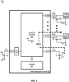
- controller 322 are configured to cause DC-to-DC converter 320 to quickly switch between energy transfer modes. For example, particular embodiments of controller 322 are configured to cause DC-to-DC converter 320 to repeatedly switch between input energy transfer mode 402 and one or more output energy transfer modes 502, such as to simultaneously regulate both voltage V T and one or more load voltages V L under light load conditions of electrical system 300. Additionally, certain embodiments of controller 322 are configured to give an output energy transfer mode 502 priority over input energy transfer mode 402 to promote accurate regulation of load voltage V L and/or load current I L .
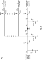
- Buck-boost converter 900 includes an input capacitor 902, a switching device 904, a switching device 906, a switching device 908, a switching device 910, N switching devices 912, and an inductor 914.
- Inductor 914 is an embodiment of inductor 324 ( FIG. 3 )
- Switching devices 904, 906, 908, 912 and 912 are controlled by respective control signals ⁇ 1, ⁇ 2, ⁇ 3, ⁇ 4, and ⁇ 5, generated by controller 322 (not shown in FIG. 9 ).
- each switching device 904, 906, 908, 912 and 912 includes one or more transistors, and each switching device 904, 906, 908, 912 and 912 optionally further includes driving circuitry for driving the one or more transistors.
- Input capacitor 902 is electrically coupled between first input port 312 and reference node 318, and switching device 904 is electrically coupled between first input port 312 and a first switching node 916.
- Switching device 906 is electrically coupled between first switching node 916 and reference node 318, and inductor 914 is electrically coupled between first switching node 916 and a second switching node 918.
- Switching device 908 is electrically coupled between second switching node 918 and reference node 318, and switching device 910 is electrically coupled between second switching node 918 and second input port 314.
- Each switching device 912 is electrically coupled between first switching node 916 and a respective output port 316.
- Each switching device 904-912 of buck-boost converter 900 is not necessarily used in each energy transfer mode.
- switching devices 912 remain in their off-states in input energy transfer mode 402.
- switching device 904 remains in its off-state in any output energy transfer mode 502 as well as in any discharge energy transfer mode 702.
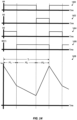
- controller 322 may generate control signals ⁇ 1, ⁇ 2, ⁇ 3, ⁇ 4, and ⁇ 5, to control operation of buck-boost converter 900. It is understood, though, that buck-boost converter 900 is not limited in operating according to examples of FIGS. 10-17 .
- phase P2 a switching devices 904 and 910 are in their on-states, and switching devices 906 and 908 are in their off-states. Consequently, voltage V ind across inductor 914 is equal to V bat - V T . Voltage V es is greater than voltage V T in the FIG. 10 example, and current I ind therefore continues to ramp upward in phase P2 a , albeit at a slower rate than in phase P1 a . Inductor 914 continues to be charged with energy from energy source 304, as well as deliver energy to capacitor 306, in phase P2 a . In phase P3 a , switching devices 906 and 910 are in their on-states, and switching devices 904 and 908 are in their off-states.
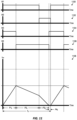
- FIG. 11 illustrates another example of controller 322 generating control signals ⁇ 1, ⁇ 2, ⁇ 3, and ⁇ 4 to cause buck-boost converter 900 to operate in input energy transfer mode 402.
- FIG. 11 includes graphs 1100, 1102, 1104, 1106, and 1108 which are analogous to graphs 1000, 1002, 1004, 1006, and 1008 of FIG. 10 , respectively.
- Controller 322 has a period T b , and each period T b is broken up into four phases P1 b , P2 b , P3 b , and P4 b , in the FIG. 11 example.
- Controller 322 determines relative durations of the phases of period T b , for example, to regulate one or more parameters of electrical system 300.
- phase P1 b switching devices 904 and 908 are in their on-states, and switching devices 906 and 910 are in their off-states. Consequently, voltage V ind across inductor 914 is equal to V es , and inductor 914 is charged with energy from energy source 304.
- phase P2 b switching devices 904 and 910 are in their on-states, and switching devices 906 and 908 are in their off-states. Consequently, voltage V ind across inductor 914 is equal to V es - V T .
- voltage V es is less than voltage V T in the FIG. 11 example, and current I ind therefore ramps downward in phase P2 b .
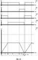
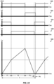
- FIG. 12 illustrates an additional example of controller 322 generating control signals ⁇ 1, ⁇ 2, ⁇ 3, and ⁇ 4 to cause buck-boost converter 900 to operate in input energy transfer mode 402.
- FIG. 12 includes graphs 1200, 1202, 1204, 1206, and 1208 which are analogous to graphs 1000, 1002, 1004, 1006, and 1008 of FIG. 10 , respectively.
- Controller 322 has a period T c , and each period T c is broken up into four phases P1 c , P2 c , P3 c , and P4 c , in the FIG. 12 example.
- Controller 322 determines relative durations of the phases of period T c , for example, to regulate one or more parameters of electrical system 300.
- phase P1 c switching devices 904 and 908 are in their on-states, and switching devices 906 and 910 are in their off-states. Consequently, voltage V ind across inductor 914 is equal to V es , and inductor 914 is charged with energy from energy source 304.
- phase P2 c switching devices 904 and 910 are in their on-states, and switching devices 906 and 908 are in their off-states. Consequently, voltage V ind across inductor 914 is equal to V bat - V T .
- voltage V es is equal to voltage V T in the FIG. 11 example, and current I ind is therefore flat in phase P2 c .
- Graph 1300 illustrates control signal ⁇ 4 versus time
- graph 1302 illustrates control signal ⁇ 3 versus time
- graph 1304 illustrates control signal ⁇ 2 versus time
- graph 1306 illustrates control signal ⁇ 5(1) versus time
- graph 1308 illustrates inductor current I ind versus time.
- Graphs 1300-1308 have a common time base.
- Controller 322 has a switching period T d , and each period T d is broken up into four phases Ph, P2 d , P3 d , and P4 d , in the FIG. 13 example.
- Controller 322 determines relative durations of the phases of period T d , for example, to regulate one or more parameters of electrical system 300.
- inductor current I ind is negative in the FIG. 13 example due to the direction of energy flow in output energy transfer mode 502(1), i.e., energy flows away from capacitor 306, instead of to capacitor 306, in output energy transfer mode 502(1).
- phase P1 d switching devices 910 and 906 are in their on-states, and switching devices 908 and 912(1) are in their off-states. Consequently, a voltage V ind across inductor 914 is equal to -V T , inductor current I ind ramps downward, and inductor 914 is charged with energy from capacitor 306.
- phase P2 d switching devices 910 and 912(1) are in their on-states, and switching devices 908 and 906 are in their off-states. Consequently, voltage V ind across inductor 914 is equal to V L (1) - V T . Voltage V T is greater than voltage V L (1) in the FIG.
- phase P3 d switching devices 908 and 912(1) are in their on-states, and switching devices 910 and 906 are in their off-states.
- FIG. 14 includes graphs 1400, 1402, 1404, 1406, and 1408 illustrating an example of controller 322 generating control signals ⁇ 4, ⁇ 3, ⁇ 2, and ⁇ 5(1) to cause buck-boost converter 900 to operate in discharge energy transfer mode 702(1) where buck-boost converter 900 transfers energy from output port 316(1) to second input port 314.
- Switching device 904 remains in its off-state in discharge energy transfer mode 702(1), and control signal ⁇ 1 is therefore not shown in FIG. 14 .
- N is greater than one
- all switching devices 912 except for switching device 912(1) also remain in their off-states in discharge energy transfer mode 702(1). Therefore, no control signals ⁇ 5 other than control signal ⁇ 5(1) are shown in FIG. 14 .
- phase P1 e switching devices 910 and 906 are in their on-states, and switching devices 908 and 912(1) are in their off-states. Consequently, a voltage V ind across inductor 914 is equal to -V T , inductor current I ind ramps downward, and capacitor 306 is charged with energy from inductor 914.
- phase P2 e switching devices 910 and 912(1) are in their on-states, and switching devices 908 and 906 are in their off-states. Consequently, voltage V ind across inductor 914 is equal to V L (1) - V T . Voltage V T is greater than voltage V L (1) in the FIG.
- FIGS. 10-15 could be modified, such as to omit one or more phases per period, add one or more phases per period, change characteristics of inductor current I ind (e.g., cause inductor current I ind to be continuous, cause inductor current I ind to be discontinuous, cause inductor current I ind to change directions, etc.).
- a third phase is omitted, such as in cases where a voltage at a port receiving is energy is greater than a voltage at a port providing energy. For instance, FIG.
- FIG. 16 illustrates an additional example of controller 322 generating control signals ⁇ 1, ⁇ 2, ⁇ 3, and ⁇ 4 to cause buck-boost converter 900 to operate in input energy transfer mode 402.
- the example of FIG. 16 is similar to the example of FIG. 11 , but with a third phase omitted.
- FIG. 16 includes graphs 1600, 1602, 1604, 1606, and 1608 which are analogous to graphs 1000, 1002, 1004, 1006, and 1008 of FIG. 10 , respectively.
- Controller 322 has a period T g , and each period T g is broken up into three phases P1 g , P2 g , and P4 g , in the FIG. 16 example. Controller 322 determines relative durations of the phases of period T g , for example, to regulate one or more parameters of electrical system 300.
- phase P1 g switching devices 904 and 908 are in their on-states, and switching devices 906 and 910 are in their off-states. Consequently, voltage V ind across inductor 914 is equal to V es , and inductor 914 is charged with energy from energy source 304.
- phase P4 g of FIG. 16 proceeds immediately from phase P2 g to phase P4 g , where switching devices 906 and 908 are in their on-states, and switching devices 904 and 910 are in their off-states, such that inductor 914 is short-circuited.
- phase P4 g of FIG. 16 is analogous to phase P4 b of FIG. 11 .
- FIG. 17 illustrates an alternate embodiment of the FIG. 13 example omitting a fourth phase.
- FIG. 17 includes graphs 1700, 1702, 1704, 1706, and 1708 illustrating another example of controller 322 generating controls signals ⁇ 4, ⁇ 3, ⁇ 2, and ⁇ 5(1) to cause buck-boost converter 900 to operate in output energy transfer mode 502(1) where buck-boost converter 900 transfers energy from second input port 314 to output port 316(1).
- Switching device 904 remains in its off-state in output energy transfer mode 502(1), and control signal ⁇ 1 is therefore not shown in FIG. 17 . Additionally, in embodiments where N is greater than one, all switching devices 912 except for switching device 912(1) also remain in their off-states in output energy transfer mode 502(1). Therefore, no control signals ⁇ 5 other than control signal ⁇ 5(1) are shown in FIG. 17 .
- Graph 1700 illustrates control signal ⁇ 4 versus time
- graph 1702 illustrates control signal ⁇ 3 versus time
- graph 1704 illustrates control signal ⁇ 2 versus time
- graph 1706 illustrates control signal ⁇ 5(1) versus time
- graph 1708 illustrates inductor current I ind versus time.
- Graphs 1700-1708 have a common time base.
- Controller 322 has a switching period T h , and each period T h is broken up into three phases P1 h , P2 h , and P3 h , in the FIG. 17 example.
- Controller 322 determines relative durations of the phases of period T h , for example, to regulate one or more parameters of electrical system 300. It should be noted that inductor current I ind is continuous in the FIG. 17 example.
- phase P1 h switching devices 910 and 906 are in their on-states, and switching devices 908 and 912(1) are in their off-states. Consequently, a voltage V ind across inductor 914 is equal to -V T , inductor current I ind ramps downward, and inductor 914 is charged with energy from capacitor 306.
- phase P2 h switching devices 910 and 912(1) are in their on-states, and switching devices 908 and 906 are in their off-states. Consequently, voltage V ind across inductor 914 is equal to V L (1) - V T . Voltage V T is greater than voltage V L (1) in the FIG.
- phase P2 h current I ind therefore continues to ramp downward in phase P2 h , albeit at a slower rate than in phase P1 h .
- Inductor 914 continues to be charged with energy from capacitor 306, as well as deliver energy to output port 316(1), in phase P2 h . It is understood, though, that if voltage V L (1) were instead greater than voltage V T , inductor current I ind would ramp upward, instead of ramping downward, in phase P2 h . Additionally, inductor current I ind would be flat in phase P2 h if voltage V T were equal to voltage V L (1).
- switching devices 908 and 912(1) are in their on-states, and switching devices 910 and 906 are in their off-states.
- controller 322 is configured to cause DC-to-DC converter 320 to switch between energy transfer modes at least partially in response to magnitude of voltage and/or current at a port of power management device 302 crossing a threshold value.
- FIG. 18 is a state diagram 1800 illustrating how some embodiments of controller 322 cause DC-to-DC converter 320 to transition between output energy transfer mode 502(1) and input energy transfer mode 402.
- state decision C is higher priority that state decision D, as shown in FIG. 18 by state decision C having a priority designation "1" and state decision D having a priority designation "2.” Accordingly, DC-to-DC converter 320 transitions from input energy transfer mode 402 to output energy transfer mode 502(1) whenever voltage V L (1) is less than V ref1 . On the other hand, if V L (1) is not less than V ref1 , and voltage V T is less than V ref2 , DC-to-DC converter 320 remains in input energy transfer mode 402, as illustrated in state diagram 1800.
- state diagram 1800 only addresses a transition between output energy transfer mode 502(1) and input energy transfer mode 402, state diagram 1800 could be modified to address a transition between input energy transfer mode 402 and one or more other output energy transfer modes 502. Additionally, two or more output energy transfer modes 502 could be prioritized. Furthermore, state diagram 1800 could be modified to further include one or more transitions into or out of a discharge energy transfer mode 702.
- DC-to-DC converter 320 can only transfer energy between two ports at a time. State differently, in these embodiments, DC-to-DC converter 320 can only operate in one energy transfer mode at a time. For example, DC-to-DC converter 320 cannot operate in output energy transfer mode 502(1) while operating in input energy transfer mode 402. As another example, DC-to-DC converter 320 cannot operate in output energy transfer mode 502(N) while operating in output energy transfer mode 502(1) (unless corresponding voltages V L (N) and V L (1) are identical).
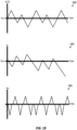
- FIG. 19 includes three graphs 1900, 1902, and 1904 illustrating one example of operation of electrical system 300 in an embodiment where controller 322 is configured to operate according to state diagram 1800 of FIG. 18 .
- Graph 1900 is of voltage V L (1) versus time
- graph 1902 is of voltage V T versus time
- graph 1904 is of inductor current I ind versus time.
- crosstalk associated with servicing second input port 314, i.e., operating DC-to-DC converter 320 in input energy transfer mode 402 to charge capacitor 306, may create significant ripple in voltage V L (1), although an average value of voltage V L (1) is approximately equal to V ref1 .
- FIG. 21 includes three graphs 2100, 2102, and 2104 illustrating one example of operation of electrical system 300 in an embodiment where controller 322 is configured to operate according to state diagram 2000 of FIG. 20 .
- Graph 2100 is of voltage V L (1) versus time
- graph 2102 is of voltage V T versus time
- graph 2104 is of inductor current I ind versus time.
- implementation of the timeout period in state diagram 2000 significantly reduced ripple of voltage V L (1), with a cost of greater variation in voltage V T , as evident when comparing graph 2102 to graph 1902 ( FIG. 19 ).
- a power management device including multiple input ports, the power management device including (1) a first input port configured to be electrically coupled to an energy source, (2) a second input port configured to be electrically coupled to a first capacitor, (3) a first output port configured to be electrically coupled to a first load, and (4) a direct-current-to-direct-current (DC-to-DC) converter configured to (i) charge the first capacitor from energy from the energy source and (ii) provide energy to the first output port at least partially using energy stored in the first capacitor.
- DC-to-DC direct-current-to-direct-current
- the DC-to-DC converter may be further configured to transfer energy stored in a second capacitor to the first capacitor, where the second capacitor is electrically coupled to the first output port.
- the DC-to-DC converter may be further configured to (1) charge the first capacitor from energy from the energy source, (2) provide energy to the first output port at least partially using energy stored in the first capacitor, and (3) transfer energy from the second capacitor to the first capacitor, using a common inductor of the DC-to-DC converter.
- the DC-to-DC converter may be further configured to (1) charge the first capacitor from energy from the energy source and (2) provide energy to the first output port at least partially using energy stored in the first capacitor, using a common inductor of the DC-to-DC converter.
- any one of the power management devices denoted as (A1) through (A4) may further include a second output port, and the DC-to-DC converter may be further configured to provide energy to the second output port at least partially using energy stored in the first capacitor.
- the DC-to-DC converter may include (1) a first switching device electrically coupled between the first input port and a first switching node, (2) a second switching device electrically coupled between the first switching node and a reference node, (3) an inductor electrically coupled between the first switching node and a second switching node, (4) a third switching device electrically coupled between the second switching node and the reference node, (5) a fourth switching device electrically coupled between the second switching node and the second input port, and (6) a fifth switching device electrically coupled between the first switching node and the first output port.
- the DC-to-DC converter may include a buck-boost converter.
- a method for powering one or more loads using a power management device includes (1) charging a first capacitor using energy from an energy source, using an inductor of a first direct-current-to-direct-current (DC-to-DC) converter, (2) providing energy to a first load from energy stored in the first capacitor, using the inductor of the first DC-to-DC converter, and (3) transferring energy stored in a second capacitor to the first capacitor, using the inductor of first DC-to-DC converter, where the second capacitor is electrically coupled to the first load.
- DC-to-DC direct-current-to-direct-current
- the method denoted as (B1) may further include limiting of magnitude of current flowing from the energy source to the first capacitor, when charging the first capacitor using energy from the energy source.
- a magnitude of a voltage across the first capacitor may be greater than a magnitude of a voltage across the energy source.
- Any one of the methods denoted as (B1) through (B3) may further include providing energy to the first load from energy stored in the first capacitor in response to a voltage at the first load crossing a first threshold value.
- Any one of the methods denoted as (B1) through (B4) may further include charging the first capacitor using energy from the energy source in response to both of (1) a voltage of the first capacitor crossing a second threshold value and (2) a timeout period expiring.
- Any one of the methods denoted as (B1) through (B5) may further include providing energy to a second load from energy stored in the first capacitor, using the inductor of the first DC-to-DC converter.
- the method denoted as (B6) may further include transferring energy stored in a third capacitor to the first capacitor, using the inductor of first DC-to-DC converter, where the third capacitor is electrically coupled to the second load.
- the energy source may include a battery.
- the energy source may include a buck-boost converter.
- An electrical system includes (1) an energy source, (2) a first capacitor, (3) a first load, and (4) a power management device.
- the power management device includes (i) a first input port electrically coupled to the energy source, (ii) a second input port electrically coupled to the first capacitor, (iii) a first output port electrically coupled to the first load, and (iv) a direct-current-to-direct-current (DC-to-DC) converter configured to (a) charge the first capacitor from energy of the energy source, and (b) provide energy to the first load at least partially using energy stored in the first capacitor.
- DC-to-DC direct-current-to-direct-current
- the DC-to-DC converter may be further configured to (a) charge the first capacitor from energy of the energy source, (b) provide energy to the first load at least partially using energy stored in the first capacitor, and (c) transfer energy from the second capacitor to the first capacitor, using a common inductor of the DC-to-DC converter.
- the DC-to-DC converter may be further configured to (a) charge the first capacitor from energy of the energy source and (b) provide energy to the first load at least partially using energy stored in the first capacitor, using a common inductor of the DC-to-DC converter.
- the electrical system may further include a second load
- the DC-to-DC converter may be further configured to provide energy to the second load at least partially using energy stored in the first capacitor.
- the DC-to-DC converter may include (1) a first switching device electrically coupled between the energy source and a first switching node, (2) a second switching device electrically coupled between the first switching node and a reference node, (3) an inductor electrically coupled between the first switching node and a second switching node, (4) a third switching device electrically coupled between the second switching node and the reference node, (5) a fourth switching device electrically coupled between the second switching node and the first capacitor, and (6) a fifth switching device electrically coupled between the first switching node and the first load.
- any one of the electrical systems denoted as (C1) through (C6) may further include a controller configured to control operation of the DC-to-DC converter at least partially according (a) a voltage across the first capacitor and (b) a voltage at the first load.
- the energy source may include a battery.
- the DC-to-DC converter may include a buck-boost converter.
Landscapes
- Engineering & Computer Science (AREA)
- Power Engineering (AREA)
- Dc-Dc Converters (AREA)
Applications Claiming Priority (2)
| Application Number | Priority Date | Filing Date | Title |
|---|---|---|---|
| US202363513084P | 2023-07-11 | 2023-07-11 | |
| US18/762,862 US20250023379A1 (en) | 2023-07-11 | 2024-07-03 | Power management devices including multiple input ports, and associated systems and methods |
Publications (1)
| Publication Number | Publication Date |
|---|---|
| EP4492658A1 true EP4492658A1 (fr) | 2025-01-15 |
Family
ID=91853208
Family Applications (1)
| Application Number | Title | Priority Date | Filing Date |
|---|---|---|---|
| EP24186671.4A Pending EP4492658A1 (fr) | 2023-07-11 | 2024-07-04 | Dispositifs de gestion d'énergie comprenant de multiples ports d'entrée, et systèmes et procédés associés |
Country Status (4)
| Country | Link |
|---|---|
| US (1) | US20250023379A1 (fr) |
| EP (1) | EP4492658A1 (fr) |
| KR (1) | KR20250009911A (fr) |
| CN (1) | CN119315658A (fr) |
Citations (1)
| Publication number | Priority date | Publication date | Assignee | Title |
|---|---|---|---|---|
| US20200409442A1 (en) * | 2019-06-25 | 2020-12-31 | Rohm Co., Ltd. | Power supply circuit and power supply voltage supply method |
-
2024
- 2024-07-03 US US18/762,862 patent/US20250023379A1/en active Pending
- 2024-07-04 EP EP24186671.4A patent/EP4492658A1/fr active Pending
- 2024-07-05 CN CN202410895861.4A patent/CN119315658A/zh active Pending
- 2024-07-05 KR KR1020240088641A patent/KR20250009911A/ko not_active Ceased
Patent Citations (1)
| Publication number | Priority date | Publication date | Assignee | Title |
|---|---|---|---|---|
| US20200409442A1 (en) * | 2019-06-25 | 2020-12-31 | Rohm Co., Ltd. | Power supply circuit and power supply voltage supply method |
Non-Patent Citations (1)
| Title |
|---|
| WU HONGFEI ET AL: "A Family of Multiport Buck-Boost Converters Based on DC-Link-Inductors (D", IEEE TRANSACTIONS ON POWER ELECTRONICS, INSTITUTE OF ELECTRICAL AND ELECTRONICS ENGINEERS, USA, vol. 30, no. 2, 1 February 2015 (2015-02-01), pages 735 - 746, XP011560847, ISSN: 0885-8993, [retrieved on 20141007], DOI: 10.1109/TPEL.2014.2307883 * |
Also Published As
| Publication number | Publication date |
|---|---|
| US20250023379A1 (en) | 2025-01-16 |
| CN119315658A (zh) | 2025-01-14 |
| KR20250009911A (ko) | 2025-01-20 |
Similar Documents
| Publication | Publication Date | Title |
|---|---|---|
| US10693302B2 (en) | DC-DC Conversion for Multi-Cell Batteries | |
| US10727747B2 (en) | Hybrid buck-boost converter | |
| US10298124B2 (en) | Hybrid DCDC power converter with increased efficiency | |
| US10790742B1 (en) | Multi-level power converter with improved transient load response | |
| US7522435B2 (en) | Power supply converter/s with controller/s responsive to voltage, current, and power | |
| US20150069958A1 (en) | Battery charger with buck-boost operation | |
| US6906497B2 (en) | Enabling circuit for avoiding negative voltage transients | |
| US6198645B1 (en) | Buck and boost switched capacitor gain stage with optional shared rest state | |
| KR20110137386A (ko) | 2차 전지 스택을 위한 전력 관리 회로 | |
| KR20170005127A (ko) | 휴대용 전자 디바이스를 위한 단일 인덕터 다중-출력 배터리 충전기 | |
| JP2009247145A (ja) | 電源システム | |
| US20230361582A1 (en) | Control circuit apparatus of battery system and battery management system | |
| US12316219B1 (en) | Switched capacitor recirculating converter circuits | |
| US6949912B2 (en) | Enabling circuit for avoiding negative voltage transients | |
| US20230275452A1 (en) | Power system, charging method, and discharging method | |
| US20180091056A1 (en) | Integrated bi-directional driver with modulated signals | |
| JP2009148110A (ja) | 充放電器とこれを用いた電源装置 | |
| CN112583102A (zh) | 一种不间断电源及充放电控制方法 | |
| US20250023379A1 (en) | Power management devices including multiple input ports, and associated systems and methods | |
| JP2003158828A (ja) | 組電池用の電圧レベル均等化装置 | |
| CN117578882B (zh) | 单模式双电流通路的降压-升压转换器的控制电路及方法 | |
| CN114498838A (zh) | 一种供电系统 | |
| JP7631638B2 (ja) | 保護回路、dc-dcコンバータ、バッテリー充電器及び電気車両 | |
| US20250088024A1 (en) | Charging systems including a multi-function dc-to-dc converter, and associated methods | |
| CN212517041U (zh) | 一种电表拉合闸电路 |
Legal Events
| Date | Code | Title | Description |
|---|---|---|---|
| PUAI | Public reference made under article 153(3) epc to a published international application that has entered the european phase |
Free format text: ORIGINAL CODE: 0009012 |
|
| STAA | Information on the status of an ep patent application or granted ep patent |
Free format text: STATUS: REQUEST FOR EXAMINATION WAS MADE |
|
| 17P | Request for examination filed |
Effective date: 20240704 |
|
| AK | Designated contracting states |
Kind code of ref document: A1 Designated state(s): AL AT BE BG CH CY CZ DE DK EE ES FI FR GB GR HR HU IE IS IT LI LT LU LV MC ME MK MT NL NO PL PT RO RS SE SI SK SM TR |