EP4495935A2 - Zusammensetzung für eine speicherzelle mit einer chalcogenverbindung, struktur davon, verfahren zur herstellung davon und verfahren zum betrieb davon - Google Patents
Zusammensetzung für eine speicherzelle mit einer chalcogenverbindung, struktur davon, verfahren zur herstellung davon und verfahren zum betrieb davon Download PDFInfo
- Publication number
- EP4495935A2 EP4495935A2 EP24217924.0A EP24217924A EP4495935A2 EP 4495935 A2 EP4495935 A2 EP 4495935A2 EP 24217924 A EP24217924 A EP 24217924A EP 4495935 A2 EP4495935 A2 EP 4495935A2
- Authority
- EP
- European Patent Office
- Prior art keywords
- layer
- electrode
- functional
- electrode line
- functional electrode
- Prior art date
- Legal status (The legal status is an assumption and is not a legal conclusion. Google has not performed a legal analysis and makes no representation as to the accuracy of the status listed.)
- Granted
Links
Images




Classifications
-
- H—ELECTRICITY
- H10—SEMICONDUCTOR DEVICES; ELECTRIC SOLID-STATE DEVICES NOT OTHERWISE PROVIDED FOR
- H10N—ELECTRIC SOLID-STATE DEVICES NOT OTHERWISE PROVIDED FOR
- H10N70/00—Solid-state devices having no potential barriers, and specially adapted for rectifying, amplifying, oscillating or switching
- H10N70/801—Constructional details of multistable switching devices
- H10N70/881—Switching materials
- H10N70/882—Compounds of sulfur, selenium or tellurium, e.g. chalcogenides
- H10N70/8825—Selenides, e.g. GeSe
-
- H—ELECTRICITY
- H10—SEMICONDUCTOR DEVICES; ELECTRIC SOLID-STATE DEVICES NOT OTHERWISE PROVIDED FOR
- H10B—ELECTRONIC MEMORY DEVICES
- H10B63/00—Resistance change memory devices, e.g. resistive RAM [ReRAM] devices
- H10B63/20—Resistance change memory devices, e.g. resistive RAM [ReRAM] devices comprising selection components having two electrodes, e.g. diodes
-
- G—PHYSICS
- G11—INFORMATION STORAGE
- G11C—STATIC STORES
- G11C13/00—Digital stores characterised by the use of storage elements not covered by groups G11C11/00, G11C23/00, or G11C25/00
- G11C13/0002—Digital stores characterised by the use of storage elements not covered by groups G11C11/00, G11C23/00, or G11C25/00 using resistive RAM [RRAM] elements
- G11C13/0004—Digital stores characterised by the use of storage elements not covered by groups G11C11/00, G11C23/00, or G11C25/00 using resistive RAM [RRAM] elements comprising amorphous/crystalline phase transition cells
-
- G—PHYSICS
- G11—INFORMATION STORAGE
- G11C—STATIC STORES
- G11C13/00—Digital stores characterised by the use of storage elements not covered by groups G11C11/00, G11C23/00, or G11C25/00
- G11C13/0002—Digital stores characterised by the use of storage elements not covered by groups G11C11/00, G11C23/00, or G11C25/00 using resistive RAM [RRAM] elements
- G11C13/0021—Auxiliary circuits
- G11C13/0069—Writing or programming circuits or methods
-
- G—PHYSICS
- G11—INFORMATION STORAGE
- G11C—STATIC STORES
- G11C13/00—Digital stores characterised by the use of storage elements not covered by groups G11C11/00, G11C23/00, or G11C25/00
- G11C13/0002—Digital stores characterised by the use of storage elements not covered by groups G11C11/00, G11C23/00, or G11C25/00 using resistive RAM [RRAM] elements
- G11C13/0021—Auxiliary circuits
- G11C13/0097—Erasing, e.g. resetting, circuits or methods
-
- H—ELECTRICITY
- H10—SEMICONDUCTOR DEVICES; ELECTRIC SOLID-STATE DEVICES NOT OTHERWISE PROVIDED FOR
- H10B—ELECTRONIC MEMORY DEVICES
- H10B63/00—Resistance change memory devices, e.g. resistive RAM [ReRAM] devices
- H10B63/10—Phase change RAM [PCRAM, PRAM] devices
-
- H—ELECTRICITY
- H10—SEMICONDUCTOR DEVICES; ELECTRIC SOLID-STATE DEVICES NOT OTHERWISE PROVIDED FOR
- H10B—ELECTRONIC MEMORY DEVICES
- H10B63/00—Resistance change memory devices, e.g. resistive RAM [ReRAM] devices
- H10B63/80—Arrangements comprising multiple bistable or multi-stable switching components of the same type on a plane parallel to the substrate, e.g. cross-point arrays
-
- H—ELECTRICITY
- H10—SEMICONDUCTOR DEVICES; ELECTRIC SOLID-STATE DEVICES NOT OTHERWISE PROVIDED FOR
- H10N—ELECTRIC SOLID-STATE DEVICES NOT OTHERWISE PROVIDED FOR
- H10N70/00—Solid-state devices having no potential barriers, and specially adapted for rectifying, amplifying, oscillating or switching
- H10N70/011—Manufacture or treatment of multistable switching devices
-
- H—ELECTRICITY
- H10—SEMICONDUCTOR DEVICES; ELECTRIC SOLID-STATE DEVICES NOT OTHERWISE PROVIDED FOR
- H10N—ELECTRIC SOLID-STATE DEVICES NOT OTHERWISE PROVIDED FOR
- H10N70/00—Solid-state devices having no potential barriers, and specially adapted for rectifying, amplifying, oscillating or switching
- H10N70/011—Manufacture or treatment of multistable switching devices
- H10N70/061—Shaping switching materials
- H10N70/063—Shaping switching materials by etching of pre-deposited switching material layers, e.g. lithography
-
- H—ELECTRICITY
- H10—SEMICONDUCTOR DEVICES; ELECTRIC SOLID-STATE DEVICES NOT OTHERWISE PROVIDED FOR
- H10N—ELECTRIC SOLID-STATE DEVICES NOT OTHERWISE PROVIDED FOR
- H10N70/00—Solid-state devices having no potential barriers, and specially adapted for rectifying, amplifying, oscillating or switching
- H10N70/011—Manufacture or treatment of multistable switching devices
- H10N70/061—Shaping switching materials
- H10N70/066—Shaping switching materials by filling of openings, e.g. damascene method
-
- H—ELECTRICITY
- H10—SEMICONDUCTOR DEVICES; ELECTRIC SOLID-STATE DEVICES NOT OTHERWISE PROVIDED FOR
- H10N—ELECTRIC SOLID-STATE DEVICES NOT OTHERWISE PROVIDED FOR
- H10N70/00—Solid-state devices having no potential barriers, and specially adapted for rectifying, amplifying, oscillating or switching
- H10N70/20—Multistable switching devices, e.g. memristors
-
- H—ELECTRICITY
- H10—SEMICONDUCTOR DEVICES; ELECTRIC SOLID-STATE DEVICES NOT OTHERWISE PROVIDED FOR
- H10N—ELECTRIC SOLID-STATE DEVICES NOT OTHERWISE PROVIDED FOR
- H10N70/00—Solid-state devices having no potential barriers, and specially adapted for rectifying, amplifying, oscillating or switching
- H10N70/20—Multistable switching devices, e.g. memristors
- H10N70/231—Multistable switching devices, e.g. memristors based on solid-state phase change, e.g. between amorphous and crystalline phases, Ovshinsky effect
-
- H—ELECTRICITY
- H10—SEMICONDUCTOR DEVICES; ELECTRIC SOLID-STATE DEVICES NOT OTHERWISE PROVIDED FOR
- H10N—ELECTRIC SOLID-STATE DEVICES NOT OTHERWISE PROVIDED FOR
- H10N70/00—Solid-state devices having no potential barriers, and specially adapted for rectifying, amplifying, oscillating or switching
- H10N70/801—Constructional details of multistable switching devices
- H10N70/821—Device geometry
-
- H—ELECTRICITY
- H10—SEMICONDUCTOR DEVICES; ELECTRIC SOLID-STATE DEVICES NOT OTHERWISE PROVIDED FOR
- H10N—ELECTRIC SOLID-STATE DEVICES NOT OTHERWISE PROVIDED FOR
- H10N70/00—Solid-state devices having no potential barriers, and specially adapted for rectifying, amplifying, oscillating or switching
- H10N70/801—Constructional details of multistable switching devices
- H10N70/821—Device geometry
- H10N70/826—Device geometry adapted for essentially vertical current flow, e.g. sandwich or pillar type devices
-
- H—ELECTRICITY
- H10—SEMICONDUCTOR DEVICES; ELECTRIC SOLID-STATE DEVICES NOT OTHERWISE PROVIDED FOR
- H10N—ELECTRIC SOLID-STATE DEVICES NOT OTHERWISE PROVIDED FOR
- H10N70/00—Solid-state devices having no potential barriers, and specially adapted for rectifying, amplifying, oscillating or switching
- H10N70/801—Constructional details of multistable switching devices
- H10N70/841—Electrodes
-
- H—ELECTRICITY
- H10—SEMICONDUCTOR DEVICES; ELECTRIC SOLID-STATE DEVICES NOT OTHERWISE PROVIDED FOR
- H10N—ELECTRIC SOLID-STATE DEVICES NOT OTHERWISE PROVIDED FOR
- H10N70/00—Solid-state devices having no potential barriers, and specially adapted for rectifying, amplifying, oscillating or switching
- H10N70/801—Constructional details of multistable switching devices
- H10N70/881—Switching materials
- H10N70/882—Compounds of sulfur, selenium or tellurium, e.g. chalcogenides
-
- G—PHYSICS
- G11—INFORMATION STORAGE
- G11C—STATIC STORES
- G11C13/00—Digital stores characterised by the use of storage elements not covered by groups G11C11/00, G11C23/00, or G11C25/00
- G11C13/0002—Digital stores characterised by the use of storage elements not covered by groups G11C11/00, G11C23/00, or G11C25/00 using resistive RAM [RRAM] elements
- G11C13/0021—Auxiliary circuits
- G11C13/004—Reading or sensing circuits or methods
-
- G—PHYSICS
- G11—INFORMATION STORAGE
- G11C—STATIC STORES
- G11C13/00—Digital stores characterised by the use of storage elements not covered by groups G11C11/00, G11C23/00, or G11C25/00
- G11C13/0002—Digital stores characterised by the use of storage elements not covered by groups G11C11/00, G11C23/00, or G11C25/00 using resistive RAM [RRAM] elements
- G11C13/0021—Auxiliary circuits
- G11C13/0069—Writing or programming circuits or methods
- G11C2013/0083—Write to perform initialising, forming process, electro forming or conditioning
Definitions
- the present invention relates to a method for manufacturing a memory cell containing a chalcogen compound.
- a phase-change material for storing a logic state and a two-terminal switching selector for selecting a memory cell are connected to form a memory cell
- the recent U.S. Patent No. 10134470 describes a memory device with a cross-point structure which utilizes a memory cell including a single chalcogen compound layer which simultaneously serves as a two-terminal switching selector and a memory by using a chalcogen compound instead of a phase-change material, and an operation method of the memory device.
- a memory cell 1S including a selective memory element represents logic states divided into a set state, which is a low resistance state, and a reset state, which is a high resistance state.
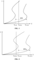
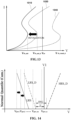
- FIG. 1 The change in current according to voltage in the memory cell 1S or 1S1P is shown in FIG. 1 , wherein a memory cell in the set state flows only a low current as the current is applied, but shows a sharp increase in current at a threshold voltage V th_set or greater, which is expressed as being turned-on.
- a memory cell in the reset state is also turned on at a threshold voltage V th_reset or greater and shows a sharp increase in current.
- the memory array has a cross-point structure including a first electrode line and a second electrode line intersecting each other, and a selective memory element disposed at each intersection of the first electrode line and the second electrode line and being a chalcogen compound, wherein the memory array includes the first electrode line formed on a substrate, a first functional electrode formed between the first electrode line and the selective memory element, and a second functional electrode formed between the second electrode line and the selective memory element, wherein the first functional electrode is formed as a line along the first electrode line.
- the applicability of the memory element to various fields can be increased.
- operational errors in the memory element including a chalcogen compound can be reduced, the accuracy of an electrical device including the memory element can be increased.
- a memory cell When a memory cell reads a logic state in a memory array with a cross-point structure including a selective memory element, as the difference between a threshold voltage of a memory cell in a set state and a threshold voltage of a memory cell in a reset state, i.e., a reading window, is stable, the probability of an error in determination is reduced.
- the first functional electrode and the second functional electrode according to the present invention are positioned between the first electrode and the second electrode intersecting each other and the selective memory element, and such functional electrodes should serve to improve characteristics of the selective memory while having characteristics of a conductive material (including a material having conductivity only under certain conditions), and at the same time, have the function of serving as a diffusion barrier of elements between the two electrodes and the selective memory element, preferably.
- a method for manufacturing a memory array with a cross-point structure including a selective memory element including (a) depositing a first electrode layer on a substrate, (b) depositing a first functional electrode layer on the first electrode layer, (c) etching the first electrode layer and the first functional electrode layer together to form a first electrode line and a first functional electrode line, (d) depositing a first ILD layer on a substrate on which the first electrode line and the first functional electrode line are formed, (e) a first planarization step of planarizing the first ILD layer to form a first surface in which at least a portion of an upper surface of the first functional electrode line is exposed between the planarized first ILD layers when viewed from an upper surface, (f) depositing a second inter-layer dielectric (ILD) layer on the first surface, (g) a hole forming step of forming a hole on the second ILD layer through etching, wherein the hole is formed on the first functional electrode line, and (ILD)
- the first ILD layer may be an oxide
- the second ILD layer may be a nitride.
- the first ILD layer may be formed of a general insulating material such as a silicon oxide or an aluminum oxide
- the second ILD layer having a large contact area with the selective memory device, which is a chalcogen compound may be formed of a nitride which is stable, thereby having low reactivity, for example, TiN, TaN, or CN to reduce the possibility of reaction with the selective memory element.
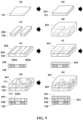
- FIG. 8 An example of a typical general method for manufacturing a memory array with a cross-point structure is shown in FIG. 8 .
- a first electrode layer 111, a first functional electrode layer 211, a chalcogen layer 311 constituting a selective memory element, and a second first electrode layer 221 are sequentially deposited and formed (Step 1), and all of them are simultaneously etched to form a wall 412 composed of a first functional electrode line 212, a chalcogen line 312, and a second functional electrode line 222, and a first electrode line 112 (Step 2).
- a first ILD layer 611 is stacked thereon (Step 3) and planarized to form a first planarization surface 611a exposing an upper surface 222a of a second functional electrode line 222 (Step 4).
- a second electrode layer 121 is deposited (Step 5) and etched to form a second electrode line 122, and at this time, etching is performed along the second electrode line 122 to a first functional electrode 213 to form a pillar 413 composed of a first functional electrode 213-a selective memory element 313-a second functional electrode 223 (Step 6).
- a second ILD layer 621 is deposited thereon to allow the second ILD layer to be filled between pillars (Step 7).
- the chalcogen layer 311 is prone to damage and forms the high wall 412 and the pillar 413 which are not supported by the surrounding, and due to characteristics of a chalcogen compound with poor rigidity, the wall 412 and the pillar 416 having such a high aspect ratio may be damaged during the process or have reduced accuracy.
- the present invention proposes a method for manufacturing a memory array with a cross-point structure using the damascene process.
- a second ILD layer 641 is deposited on the first surface 632a thus formed.
- a hole 711 is formed on the second ILD layer 641 through etching, and the hole 711 is formed on the upper surface 232a of the first functional electrode line 232.
- a chalcogen compound layer 321 constituting a selective memory element is deposited to fill the chalcogen compound into the hole, thereby forming a selective memory element 322.
- Another method relates to a structure in which a second functional electrode forms a pillar together with a selective memory element, which will be described through FIG. 11 .
- the chalcogen compound layer 311 deposited in FIG. 11 is planarized to a height lower than that of the second ILD layer 641.
- the planarization operation is referred to as an etch-back operation, and through the etch-back, the chalcogen compound layer 321 is removed from a surface other than the hole 712, and an upper surface 322b of the selective memory element 322 is independently exposed when viewed from an upper surface, wherein the height of the upper surface 322b is lower than that of the second ILD layer 641 to form a third surface 641b in which the hole 712 is still maintained on the selective memory element 322.
- a second functional electrode layer 251 is again deposited on the third surface 641b to form a second functional electrode 252 into the hole 712. Thereafter, a second electrode layer 151 is deposited, and then etched to for a second electrode line 152 for finishing.
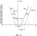
- a reading window in which the reading voltage V reading may be located in order to effectively read logic states of memory cells is changed before RW1 and after RW2 the drift.
- This change is particularly problematic in that the threshold voltages of the memory cells in the set state gradually increase, and the memory cells in the set state may be erroneously read as being in the reset state as shown in FIG. 2 .
- the threshold voltage of the memory cell 1S1P including a two-terminal selector and a phase-change memory element or the memory cell 1S including a selective memory element returns to a threshold voltage of the memory cell in an initial set state after the memory cell is turned on beyond the threshold voltage regardless of whether the memory cell is in the set state or the reset state.
- FIG. 13 shows such initialization, wherein the threshold voltage V th_set_d in a voltage-current curve 1030 of a memory cell in a set state after drift has occurred is initialized to the threshold voltage V th_set in a voltage-current curve 1010 of a memory cell in a set state before the drift after an initialization voltage V pr is applied and turn-on is achieved.
- a first initialization voltage V pre1 is applied to a memory cell in which drift has occurred and whether the memory cell is turned-on is determined.
- the initialization process is terminated when an increased initialization voltage exceeds a first voltage V1, and the first voltage V1 is within the drift reading window range RW2, which is a voltage range between a minimum threshold voltage V41 of a memory cell in the reset state expected after the drift and a maximum threshold voltage V32 of the memory cell in the set state expected after the drift. Accordingly, since the initialization voltage is greater than the maximum threshold voltage V32 in the set state, all memory cells in the set state may be turned-on, and since it does not exceed the minimum threshold voltage V41 of the memory cell stably in the reset state, a memory cell in the reset state is prevented from being turned-on and the memory cell in the reset state is not initialized.
- the initialization voltage for initializing a memory cell in the set state according to the initialization method of the present invention is only slightly higher than a threshold voltage of the memory cell, so that a load applied to the memory cell due to the initialization process may be very small. If the initialization is performed with a voltage which is too high, a memory cell is abruptly turned-on to allow a very large current to flow at once, so that the memory cell may be damaged.
- the initialization voltage may be increased by 5 to 200 mV at a time.
- a preferred voltage increase is 5 to 200 mV at a time, more preferably 20 to 60 mV.
- a first voltage is in the range of a drift reading window
- the difference between the first voltage and a maximum threshold voltage of a memory cell in a set state expected after the drift may be in the range of 0.50 to 0.95 with respect to the drift reading window.
- the first voltage V1 is within the drift reading window range RW2 and is close to the minimum threshold voltage 41 of the memory cell in the reset state expected after the drift in order to initialize all memory cells in a set state in which a threshold voltage is abnormally high, which may be possible.
- a difference A between the first voltage V1 and the maximum threshold voltage V32 of the memory cell in the set state expected after the drift is in the range of 0.50 to 0.95 when the entire drift leading window RW2 is 1.
- the first voltage V1 is close to the maximum threshold voltage V32 of the memory cell in the set state after the drift since the value is less than 0.50, it is not preferable since the memory cell in the set state having an abnormally large threshold voltage may not be initialized, and when positioned as close as possible, but too close to the minimum threshold voltage V41 of the memory cell in the reset state, it is also not preferable since the cell in the reset state may be initialized.
Landscapes
- Engineering & Computer Science (AREA)
- Manufacturing & Machinery (AREA)
- Chemical & Material Sciences (AREA)
- Crystallography & Structural Chemistry (AREA)
- Semiconductor Memories (AREA)
Applications Claiming Priority (3)
| Application Number | Priority Date | Filing Date | Title |
|---|---|---|---|
| US201962935675P | 2019-11-15 | 2019-11-15 | |
| EP20887674.8A EP4060755B1 (de) | 2019-11-15 | 2020-11-13 | Verfahren zur initialisierung einer speicherzelle mit chalkogenverbindung |
| PCT/KR2020/015992 WO2021096288A1 (ko) | 2019-11-15 | 2020-11-13 | 칼코겐 화합물을 포함하는 메모리 셀을 위한 조성물, 구조, 제조 방법 및 작동 방법 |
Related Parent Applications (2)
| Application Number | Title | Priority Date | Filing Date |
|---|---|---|---|
| EP20887674.8A Division EP4060755B1 (de) | 2019-11-15 | 2020-11-13 | Verfahren zur initialisierung einer speicherzelle mit chalkogenverbindung |
| EP20887674.8A Division-Into EP4060755B1 (de) | 2019-11-15 | 2020-11-13 | Verfahren zur initialisierung einer speicherzelle mit chalkogenverbindung |
Publications (3)
| Publication Number | Publication Date |
|---|---|
| EP4495935A2 true EP4495935A2 (de) | 2025-01-22 |
| EP4495935A3 EP4495935A3 (de) | 2025-03-12 |
| EP4495935B1 EP4495935B1 (de) | 2026-04-22 |
Family
ID=75913102
Family Applications (2)
| Application Number | Title | Priority Date | Filing Date |
|---|---|---|---|
| EP20887674.8A Active EP4060755B1 (de) | 2019-11-15 | 2020-11-13 | Verfahren zur initialisierung einer speicherzelle mit chalkogenverbindung |
| EP24217924.0A Active EP4495935B1 (de) | 2019-11-15 | 2020-11-13 | Verfahren zur herstellung eines einer chalcogenverbindung enthaltenden speicherarrays |
Family Applications Before (1)
| Application Number | Title | Priority Date | Filing Date |
|---|---|---|---|
| EP20887674.8A Active EP4060755B1 (de) | 2019-11-15 | 2020-11-13 | Verfahren zur initialisierung einer speicherzelle mit chalkogenverbindung |
Country Status (5)
| Country | Link |
|---|---|
| US (1) | US12268104B2 (de) |
| EP (2) | EP4060755B1 (de) |
| KR (1) | KR102626726B1 (de) |
| CN (1) | CN114730835B (de) |
| WO (1) | WO2021096288A1 (de) |
Families Citing this family (4)
| Publication number | Priority date | Publication date | Assignee | Title |
|---|---|---|---|---|
| WO2023024012A1 (en) * | 2021-08-26 | 2023-03-02 | Yangtze Memory Technologies Co., Ltd. | Three-dimensional nand memory and fabrication method thereof |
| US12588218B2 (en) | 2022-04-11 | 2026-03-24 | Samsung Electronics Co., Ltd. | Chalcogenide material, switching device including the chalcogenide material, and memory device including the switching device |
| KR20240080367A (ko) * | 2022-11-30 | 2024-06-07 | 에스케이하이닉스 주식회사 | 칼코게나이드 물질 및 반도체 장치 |
| KR102880082B1 (ko) * | 2024-02-28 | 2025-11-03 | 인텔리전트 에이치 떠블유 아이엔씨 | 스위칭 특성을 가지는 메모리 소자 및 그 작동 방법 |
Citations (1)
| Publication number | Priority date | Publication date | Assignee | Title |
|---|---|---|---|---|
| US10134470B2 (en) | 2015-11-04 | 2018-11-20 | Micron Technology, Inc. | Apparatuses and methods including memory and operation of same |
Family Cites Families (32)
| Publication number | Priority date | Publication date | Assignee | Title |
|---|---|---|---|---|
| US7220982B2 (en) * | 2004-07-27 | 2007-05-22 | Micron Technology, Inc. | Amorphous carbon-based non-volatile memory |
| US7135696B2 (en) * | 2004-09-24 | 2006-11-14 | Intel Corporation | Phase change memory with damascene memory element |
| US20060255328A1 (en) * | 2005-05-12 | 2006-11-16 | Dennison Charles H | Using conductive oxidation for phase change memory electrodes |
| JP4371149B2 (ja) * | 2007-01-09 | 2009-11-25 | ソニー株式会社 | 半導体メモリデバイス、センスアンプ回路、および、メモリセルの読み出し方法 |
| US8120951B2 (en) * | 2008-05-22 | 2012-02-21 | Micron Technology, Inc. | Memory devices, memory device constructions, constructions, memory device forming methods, current conducting devices, and memory cell programming methods |
| US8081506B2 (en) * | 2009-12-14 | 2011-12-20 | Intel Corporation | Amorphous semiconductor threshold switch volatile memory cell |
| US8649212B2 (en) * | 2010-09-24 | 2014-02-11 | Intel Corporation | Method, apparatus and system to determine access information for a phase change memory |
| US8486743B2 (en) * | 2011-03-23 | 2013-07-16 | Micron Technology, Inc. | Methods of forming memory cells |
| KR20120137862A (ko) * | 2011-06-13 | 2012-12-24 | 삼성전자주식회사 | 3차원 더블 크로스 포인트 어레이를 갖는 반도체 메모리 소자 및 그 제조방법 |
| US9021227B2 (en) * | 2011-06-22 | 2015-04-28 | Intel Corporation | Drift management in a phase change memory and switch (PCMS) memory device |
| US9166158B2 (en) * | 2013-02-25 | 2015-10-20 | Micron Technology, Inc. | Apparatuses including electrodes having a conductive barrier material and methods of forming same |
| US9105360B2 (en) * | 2013-03-07 | 2015-08-11 | Seagate Technology Llc | Forming a characterization parameter of a resistive memory element |
| US8971093B2 (en) * | 2013-05-14 | 2015-03-03 | Kabushiki Kaisha Toshiba | Memory device and method of controlling memory device |
| US9306165B2 (en) * | 2014-03-27 | 2016-04-05 | Micron Technology, Inc. | Replacement materials processes for forming cross point memory |
| US9275730B2 (en) * | 2014-04-11 | 2016-03-01 | Micron Technology, Inc. | Apparatuses and methods of reading memory cells based on response to a test pulse |
| US9299430B1 (en) * | 2015-01-22 | 2016-03-29 | Nantero Inc. | Methods for reading and programming 1-R resistive change element arrays |
| US9613691B2 (en) * | 2015-03-27 | 2017-04-04 | Intel Corporation | Apparatus and method for drift cancellation in a memory |
| US10115461B1 (en) * | 2016-05-25 | 2018-10-30 | SK Hynix Inc. | Electronic device using resistive memory element and a recovery operation to compensate for threshold drift |
| JP2017224688A (ja) * | 2016-06-14 | 2017-12-21 | ソニー株式会社 | 回路素子、記憶装置、電子機器、回路素子への情報の書き込み方法、および回路素子からの情報の読み出し方法 |
| US9824767B1 (en) * | 2016-06-29 | 2017-11-21 | Intel Corporation | Methods and apparatus to reduce threshold voltage drift |
| KR102571566B1 (ko) * | 2016-07-15 | 2023-08-29 | 삼성전자주식회사 | 반도체 메모리 장치 |
| US11183633B2 (en) * | 2016-10-04 | 2021-11-23 | Sony Semiconductor Solutions Corporation | Switch device, storage apparatus, and memory system |
| KR102657562B1 (ko) * | 2016-12-02 | 2024-04-17 | 에스케이하이닉스 주식회사 | 비휘발성 메모리 장치 |
| US10672833B2 (en) * | 2017-07-26 | 2020-06-02 | Micron Technology, Inc. | Semiconductor devices including a passive material between memory cells and conductive access lines, and related electronic devices |
| US10510957B2 (en) * | 2017-07-26 | 2019-12-17 | Micron Technology, Inc. | Self-aligned memory decks in cross-point memory arrays |
| US10566052B2 (en) * | 2017-12-22 | 2020-02-18 | Micron Technology, Inc. | Auto-referenced memory cell read techniques |
| US10424730B2 (en) * | 2018-02-09 | 2019-09-24 | Micron Technology, Inc. | Tapered memory cell profiles |
| US10290348B1 (en) * | 2018-02-12 | 2019-05-14 | Sandisk Technologies Llc | Write-once read-many amorphous chalcogenide-based memory |
| DE112019001105T5 (de) * | 2018-03-02 | 2020-11-12 | Sony Semiconductor Solutions Corporation | Schaltvorrichtung, speicherungseinrichtung und speichersystem |
| KR102571555B1 (ko) * | 2018-08-28 | 2023-08-29 | 삼성전자주식회사 | 가변 저항 메모리 소자 |
| US11049557B2 (en) * | 2019-07-19 | 2021-06-29 | Macronix International Co., Ltd. | Leakage current compensation in crossbar array |
| US10943657B1 (en) * | 2019-08-19 | 2021-03-09 | Micron Technology, Inc. | Mitigation of voltage threshold drift associated with power down condition of non-volatile memory device |
-
2020
- 2020-11-13 EP EP20887674.8A patent/EP4060755B1/de active Active
- 2020-11-13 CN CN202080078617.9A patent/CN114730835B/zh active Active
- 2020-11-13 US US17/774,191 patent/US12268104B2/en active Active
- 2020-11-13 EP EP24217924.0A patent/EP4495935B1/de active Active
- 2020-11-13 KR KR1020227015179A patent/KR102626726B1/ko active Active
- 2020-11-13 WO PCT/KR2020/015992 patent/WO2021096288A1/ko not_active Ceased
Patent Citations (1)
| Publication number | Priority date | Publication date | Assignee | Title |
|---|---|---|---|---|
| US10134470B2 (en) | 2015-11-04 | 2018-11-20 | Micron Technology, Inc. | Apparatuses and methods including memory and operation of same |
Also Published As
| Publication number | Publication date |
|---|---|
| KR20220083726A (ko) | 2022-06-20 |
| US12268104B2 (en) | 2025-04-01 |
| EP4060755C0 (de) | 2025-08-06 |
| EP4495935B1 (de) | 2026-04-22 |
| US20220367808A1 (en) | 2022-11-17 |
| CN114730835A (zh) | 2022-07-08 |
| CN114730835B (zh) | 2025-08-29 |
| EP4060755B1 (de) | 2025-08-06 |
| EP4060755A4 (de) | 2024-05-29 |
| WO2021096288A1 (ko) | 2021-05-20 |
| EP4060755A1 (de) | 2022-09-21 |
| KR102626726B1 (ko) | 2024-01-17 |
| EP4495935A3 (de) | 2025-03-12 |
Similar Documents
| Publication | Publication Date | Title |
|---|---|---|
| EP4495935B1 (de) | Verfahren zur herstellung eines einer chalcogenverbindung enthaltenden speicherarrays | |
| CN101615425B (zh) | 具有双重字线和源极线的相变化存储器及其操作方法 | |
| US20210151676A1 (en) | Semiconductor devices comprising threshold switching materials | |
| US10186658B2 (en) | Memory device and method of manufacturing memory device | |
| US7608848B2 (en) | Bridge resistance random access memory device with a singular contact structure | |
| CN100593865C (zh) | 对一主动侧壁相变存储单元改善热绝缘的结构及方法 | |
| US8890109B2 (en) | Resistive random access memory access cells having thermally isolating structures | |
| US8304754B2 (en) | Metal oxide materials and electrodes for Re-RAM | |
| US7919766B2 (en) | Method for making self aligning pillar memory cell device | |
| US20110163288A1 (en) | Manufacturing Method for Pipe-Shaped Electrode Phase Change Memory | |
| US20080173931A1 (en) | Multilevel-Cell Memory Structures Employing Multi-Memory Layers with Tungsten Oxides and Manufacturing Method | |
| KR20000052840A (ko) | 상 전이(phase-change)메모리 물질과 유전체 물질의 혼합물을 포함하는 복합 메모리 재료 | |
| CN101783390A (zh) | 具有改善结构稳定性的存储单元及其制造方法 | |
| US11683940B2 (en) | Method of manufacturing variable resistance memory device | |
| US20250344406A1 (en) | Switching cell | |
| KR20220021550A (ko) | 정보 저장 물질 패턴 및 셀렉터 물질 패턴을 포함하는 반도체 장치 | |
| US10692931B2 (en) | Electronic device and method for fabricating the same | |
| US20200066988A1 (en) | Electronic device and method for fabricating the same | |
| CN110034110A (zh) | 包含电阻随机存取存储器和选择器的基本单元和包含该单元的级和级的基体及其制造方法 | |
| KR20220128111A (ko) | 가변 저항 메모리 장치 | |
| KR20250112592A (ko) | 가변 저항 메모리 소자 및 그 제조 방법 | |
| CN116634853A (zh) | 阻变存储器及其制备方法 |
Legal Events
| Date | Code | Title | Description |
|---|---|---|---|
| PUAI | Public reference made under article 153(3) epc to a published international application that has entered the european phase |
Free format text: ORIGINAL CODE: 0009012 |
|
| STAA | Information on the status of an ep patent application or granted ep patent |
Free format text: STATUS: THE APPLICATION HAS BEEN PUBLISHED |
|
| AC | Divisional application: reference to earlier application |
Ref document number: 4060755 Country of ref document: EP Kind code of ref document: P |
|
| AK | Designated contracting states |
Kind code of ref document: A2 Designated state(s): AL AT BE BG CH CY CZ DE DK EE ES FI FR GB GR HR HU IE IS IT LI LT LU LV MC MK MT NL NO PL PT RO RS SE SI SK SM TR |
|
| REG | Reference to a national code |
Ref country code: DE Ref legal event code: R079 Free format text: PREVIOUS MAIN CLASS: G11C0013000000 Ipc: H10N0070000000 Ref document number: 602020071024 Country of ref document: DE |
|
| PUAL | Search report despatched |
Free format text: ORIGINAL CODE: 0009013 |
|
| AK | Designated contracting states |
Kind code of ref document: A3 Designated state(s): AL AT BE BG CH CY CZ DE DK EE ES FI FR GB GR HR HU IE IS IT LI LT LU LV MC MK MT NL NO PL PT RO RS SE SI SK SM TR |
|
| RIC1 | Information provided on ipc code assigned before grant |
Ipc: H10B 63/10 20230101ALI20250131BHEP Ipc: G11C 13/00 20060101ALI20250131BHEP Ipc: H10B 63/00 20230101ALI20250131BHEP Ipc: H10N 70/20 20230101ALI20250131BHEP Ipc: H10N 70/00 20230101AFI20250131BHEP |
|
| STAA | Information on the status of an ep patent application or granted ep patent |
Free format text: STATUS: REQUEST FOR EXAMINATION WAS MADE |
|
| 17P | Request for examination filed |
Effective date: 20250626 |
|
| GRAP | Despatch of communication of intention to grant a patent |
Free format text: ORIGINAL CODE: EPIDOSNIGR1 |
|
| STAA | Information on the status of an ep patent application or granted ep patent |
Free format text: STATUS: GRANT OF PATENT IS INTENDED |
|
| INTG | Intention to grant announced |
Effective date: 20251208 |
|
| RAP1 | Party data changed (applicant data changed or rights of an application transferred) |
Owner name: IHW INC. |
|
| GRAS | Grant fee paid |
Free format text: ORIGINAL CODE: EPIDOSNIGR3 |
|
| GRAA | (expected) grant |
Free format text: ORIGINAL CODE: 0009210 |
|
| STAA | Information on the status of an ep patent application or granted ep patent |
Free format text: STATUS: THE PATENT HAS BEEN GRANTED |
|
| AC | Divisional application: reference to earlier application |
Ref document number: 4060755 Country of ref document: EP Kind code of ref document: P |
|
| AK | Designated contracting states |
Kind code of ref document: B1 Designated state(s): AL AT BE BG CH CY CZ DE DK EE ES FI FR GB GR HR HU IE IS IT LI LT LU LV MC MK MT NL NO PL PT RO RS SE SI SK SM TR |
|
| REG | Reference to a national code |
Ref country code: CH Ref legal event code: F10 Free format text: ST27 STATUS EVENT CODE: U-0-0-F10-F00 (AS PROVIDED BY THE NATIONAL OFFICE) Effective date: 20260422 Ref country code: GB Ref legal event code: FG4D |