EP4496009A1 - Verfahren zur herstellung eines hallelements und magnetisches speicherelement - Google Patents
Verfahren zur herstellung eines hallelements und magnetisches speicherelement Download PDFInfo
- Publication number
- EP4496009A1 EP4496009A1 EP23774597.1A EP23774597A EP4496009A1 EP 4496009 A1 EP4496009 A1 EP 4496009A1 EP 23774597 A EP23774597 A EP 23774597A EP 4496009 A1 EP4496009 A1 EP 4496009A1
- Authority
- EP
- European Patent Office
- Prior art keywords
- substrate
- magnetic material
- material layer
- hall element
- perovskite
- Prior art date
- Legal status (The legal status is an assumption and is not a legal conclusion. Google has not performed a legal analysis and makes no representation as to the accuracy of the status listed.)
- Pending
Links
Images


Classifications
-
- H—ELECTRICITY
- H10—SEMICONDUCTOR DEVICES; ELECTRIC SOLID-STATE DEVICES NOT OTHERWISE PROVIDED FOR
- H10N—ELECTRIC SOLID-STATE DEVICES NOT OTHERWISE PROVIDED FOR
- H10N52/00—Hall-effect devices
- H10N52/01—Manufacture or treatment
-
- H—ELECTRICITY
- H10—SEMICONDUCTOR DEVICES; ELECTRIC SOLID-STATE DEVICES NOT OTHERWISE PROVIDED FOR
- H10B—ELECTRONIC MEMORY DEVICES
- H10B61/00—Magnetic memory devices, e.g. magnetoresistive RAM [MRAM] devices
-
- H—ELECTRICITY
- H10—SEMICONDUCTOR DEVICES; ELECTRIC SOLID-STATE DEVICES NOT OTHERWISE PROVIDED FOR
- H10N—ELECTRIC SOLID-STATE DEVICES NOT OTHERWISE PROVIDED FOR
- H10N52/00—Hall-effect devices
- H10N52/101—Semiconductor Hall-effect devices
-
- H—ELECTRICITY
- H10—SEMICONDUCTOR DEVICES; ELECTRIC SOLID-STATE DEVICES NOT OTHERWISE PROVIDED FOR
- H10N—ELECTRIC SOLID-STATE DEVICES NOT OTHERWISE PROVIDED FOR
- H10N52/00—Hall-effect devices
- H10N52/80—Constructional details
-
- H—ELECTRICITY
- H10—SEMICONDUCTOR DEVICES; ELECTRIC SOLID-STATE DEVICES NOT OTHERWISE PROVIDED FOR
- H10N—ELECTRIC SOLID-STATE DEVICES NOT OTHERWISE PROVIDED FOR
- H10N52/00—Hall-effect devices
- H10N52/80—Constructional details
- H10N52/85—Materials of the active region
Definitions
- the present invention relates to a method for manufacturing a Hall element and a magnetic memory element.
- InSb, GaAs, or InAs compounds are used as materials of a Hall element used to read information in a magnetic memory.
- An InSb element is manufactured by, for example, depositing an InSb thin film on one surface of a mica substrate and forming an electrode and a protective film on the mica substrate (see, for example, Patent Literature 1).
- Patent Literature 1 JPH6-232479
- the present invention addresses the issue described above, and a purpose thereof is to provide a technology for manufacturing a Hall element suited to read information written in a magnetic memory.
- a method of manufacturing a Hall element includes: forming a perovskite-type magnetic material layer on a substrate having a perovskite structure and composed of a compound having a lattice constant of 3.90-3.97 ⁇ in pseudocubic notation; forming an insulator layer containing SrTiO 3 on the perovskite-type magnetic material layer; and forming a Hall element containing InSb on the insulator layer.
- the magnetic memory element includes: a substrate having a perovskite structure and composed of a compound having a lattice constant of 3.90-3.97 ⁇ in pseudocubic notation; a perovskite-type magnetic material layer disposed on the substrate; an insulator layer disposed on the perovskite-type magnetic material layer and containing SrTiO 3 ; and a Hall element disposed on the insulator layer and containing InSb.
- Figs. 1A-1D are sectional views showing an example of a process for manufacturing a Hall element according to an embodiment.
- a substrate 12 is first prepared as shown in Fig. 1A .
- the substrate 12 has a perovskite structure and is composed of a compound having a lattice constant of 3.90-3.97 ⁇ in pseudocubic notation.
- Specific examples of the substrate 12 include a 110 oriented GdScO 3 substrate, a 110 oriented DyScO 3 substrate, a 110 oriented SrTiO 3 substrate, a 111 oriented SrTiO 3 substrate, and a 001 oriented SrTiO 3 substrate.
- a perovskite-type magnetic material layer (hereinafter simply referred to as a magnetic material layer) 14 is formed on the substrate 12.
- the perovskite-type magnetic material constituting the magnetic material layer 14 include La 2 NiMnO 6 , CeCu 3 Mn 4 O 12 , La 0.7 Sr 0.3 MnO 3 , etc.
- the magnetic material layer 14 is composed of a compound represented by the following formula (1).
- BiFe 1-x A x O 3 ... (1) Referring to formula (1), A denotes Co or Mn, and x satisfies 0.05 ⁇ x ⁇ 0.25. When x is 0.05 or more, the magnetic material layer 14 can exhibit ferromagnetism and ferroelectricity at room temperature. When x is less than 0.25, changes in the crystal structure of the magnetic material layer 14 can be suppressed.
- an insulator layer 16 is formed on the magnetic material layer 14.
- the insulator layer 16 contains SrTiO 3 .
- a Hall element 18 containing InSb, GaAs, InAs or a solid solution thereof is formed on the insulator layer 16.
- the magnetic material layer 14, the insulator layer 16, and the Hall element 18 may not be formed by the method described above and can be formed by a method known to those skilled in the art, such as physical vapor deposition method (PVD method) and chemical vapor deposition method (CVD method).
- PVD method physical vapor deposition method
- CVD method chemical vapor deposition method
- PVD method include pulsed laser deposition (PLD) method and electron beam deposition method
- PVD method include metal-organic (MO) CVD method and mist CVD method.
- the shapes of the substrate 12, the magnetic material layer 14, the insulator layer 16, and the Hall element 18 are not limited to those shown, and a suitable shape can be selected according to the application.
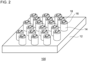
- FIG. 2 is a schematic diagram showing a configuration of an exemplary magnetic memory element according to the embodiment.
- a magnetic memory element 100 includes a substrate 12 having a perovskite structure and composed of a compound having a lattice constant of 3.90-3.97 ⁇ in pseudocubic notation, a perovskite-type magnetic material layer 14 disposed on the substrate 12, an insulator layer 16 disposed on the magnetic material layer 14, and a Hall element 18 disposed on the insulator layer 16.
- the substrate 12 has a perovskite structure and is composed of a compound having a lattice constant of 3.90-3.97 ⁇ in pseudocubic notation. Forming the magnetic material layer 14 on the substrate 12 composed of such a compound makes it possible to manifest magnetization intrinsic to the magnetic material layer 14 itself and to reverse the magnetization of the magnetic material layer 14 by applying a magnetic field or an electric field.
- Specific examples of the substrate 12 include a 110 oriented GdScO 3 substrate, a 110 oriented DyScO 3 substrate, a 110 oriented SrTiO 3 substrate, a 111 oriented SrTiO 3 substrate, and a 001 oriented SrTiO 3 substrate.
- the thickness of the substrate 12 is not particularly limited, but from the viewpoint of thin film synthesis and ease of handling, 300 ⁇ m-1000 ⁇ m is preferable, and 400 ⁇ m-600 ⁇ m is more preferable.
- the perovskite-type magnetic material layer 14 is composed of a compound represented by the following formula (1).
- BiFe 1-x A x O 3 ... (1) A denotes Co or Mn, and x satisfies 0.05 ⁇ x ⁇ 0.25.
- x is 0.05 or more, the magnetic material layer 14 can exhibit ferromagnetism and ferroelectricity at room temperature.
- x is less than 0.25, changes in the crystal structure of the magnetic material layer 14 can be suppressed.
- the magnitude of spontaneous magnetization of the magnetic material layer 14 at room temperature is about 1 emu/cm 3 -10 emu/cm 3 , and the magnitude of spontaneous polarization is about 50-150 ⁇ C/cm 2 .
- the magnetization direction of the magnetic material layer 14 composed of this compound can be reversed by an electric field generated by applying a voltage. This allows information to be written in the magnetic material layer 14. Further, the written information can be read by detecting the reversed magnetization by the Hall element 18.
- the thickness of the magnetic material layer 14 is, for example, 30 nm-1000 nm. Given such a thickness of the magnetic material layer 14, an electric field can be reliably applied to the magnetic material layer 14, and the reliability of the device can be improved. From the viewpoint of lattice distortion, the thickness of the magnetic material layer 14 is preferably 50 nm-400 nm.
- the insulator layer 16 contains SrTiO 3 .
- the thickness of the insulator layer 16 is, for example, 1 nm-50 nm. From the viewpoint of suppressing a reaction with the magnetic material layer 14 and suppressing shielding of the magnetic field from the magnetic material layer 14 by the insulator layer 16 itself, the thickness of the insulator layer 16 is preferably 2 nm-30 nm and, more preferably, 4 nm-10 nm.
- the Hall element 18 contains InSb, GaAs, InAs or a solid solution thereof.
- the shape of the Hall element 18 shown in Fig. 1 is not particularly limited and may be another shape such as a cross shape as shown in Fig. 2 and a cylindrical shape.
- the Hall element according to the embodiment was manufactured by pulsed laser deposition (PLD) method.
- a BiFe 1-x Co x O 3 (BFCO) layer (thickness 60 nm) was produced on a SrTiO 3 (001) substrate under the condition shown in Table 1.
- a SrTiO 3 (STO) insulator layer (thickness 6.7 nm) was produced on the BFCO layer, and an InSb layer (150 nm) was produced on the insulator layer.
- a Hall element was manufactured as a comparative example in the same manner as in the embodiment except that an InSb thin film was produced on a BFCO thin film without producing an STO insulator layer.
- XRD X-ray diffraction
- SmartLab SmartLab from Rigaku
- the Hall effect was measured using a physical property measurement system (from Quantum Design, Inc. in the United States).
- Fig. 3 shows X-ray diffraction measurement results of the embodiment and the comparative example.
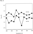
- Fig. 4 shows Hall effect measurement results of the Hall element of the embodiment.
- Table 1 Layer Substrate temperature ( °C) Oxygen partial pressure (Pa) Laser energy density (J/cm 2 ) Laser repetition frequency (Hz) BFCO 660 15 1.0 5 STO 660 15 1.0 1 InSb 250 1.3 ⁇ 10 -3 0.5-0.6 20
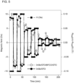
- the Hall effect of the Hall element according to the embodiment exhibited when the magnetic field is reversed multiple times at room temperature was measured using a physical property measurement system (from Quantum Design, Inc. in the United States). The results are shown in Fig. 5 . It can be seen from Fig. 5 that when the magnetic field is reversed, the sign of the Hall resistance changes, and that the Hall element functions as a sensor capable of detecting a magnetic field of 1 Oe.
- the embodiments of the present invention are not limited to those described above and appropriate combinations or replacements of the features of the embodiments are also encompassed by the present invention.
- the embodiments may be modified by way of combinations, rearranging of the processing sequence, various design changes, etc., based on the knowledge of a skilled person, and the embodiment modified as such are also within the scope of the present invention.
- the present invention can be used in a method for manufacturing a Hall element and a magnetic memory element.
Landscapes
- Engineering & Computer Science (AREA)
- Manufacturing & Machinery (AREA)
- Hall/Mr Elements (AREA)
Applications Claiming Priority (2)
| Application Number | Priority Date | Filing Date | Title |
|---|---|---|---|
| JP2022048131 | 2022-03-24 | ||
| PCT/JP2023/009333 WO2023181998A1 (ja) | 2022-03-24 | 2023-03-10 | ホール素子の製造方法及び磁気メモリ素子 |
Publications (2)
| Publication Number | Publication Date |
|---|---|
| EP4496009A1 true EP4496009A1 (de) | 2025-01-22 |
| EP4496009A4 EP4496009A4 (de) | 2026-04-01 |
Family
ID=88101322
Family Applications (1)
| Application Number | Title | Priority Date | Filing Date |
|---|---|---|---|
| EP23774597.1A Pending EP4496009A4 (de) | 2022-03-24 | 2023-03-10 | Verfahren zur herstellung eines hallelements und magnetisches speicherelement |
Country Status (6)
| Country | Link |
|---|---|
| US (1) | US20250017119A1 (de) |
| EP (1) | EP4496009A4 (de) |
| JP (1) | JP7822579B2 (de) |
| KR (1) | KR102894253B1 (de) |
| CN (1) | CN119054087A (de) |
| WO (1) | WO2023181998A1 (de) |
Families Citing this family (1)
| Publication number | Priority date | Publication date | Assignee | Title |
|---|---|---|---|---|
| WO2026004768A1 (ja) * | 2024-06-25 | 2026-01-02 | 住友化学株式会社 | シリコン基板とペロブスカイト型構造を有する化合物の薄膜との積層体、及び該積層体を有する磁気メモリ素子 |
Family Cites Families (8)
| Publication number | Priority date | Publication date | Assignee | Title |
|---|---|---|---|---|
| JP3404780B2 (ja) | 1993-02-01 | 2003-05-12 | 株式会社村田製作所 | InSb薄膜素子の製造方法 |
| US5652445A (en) * | 1995-04-21 | 1997-07-29 | Johnson; Mark B. | Hybrid hall effect device and method of operation |
| JP2001320108A (ja) * | 2000-05-02 | 2001-11-16 | Canon Inc | 磁気抵抗素子、磁気メモリ及び磁気センサー |
| WO2002016955A2 (en) * | 2000-08-18 | 2002-02-28 | Motorola, Inc. | Compound semiconductor hall sensor |
| WO2003081680A1 (en) * | 2002-03-26 | 2003-10-02 | Japan Science And Technology Agency | Tunneling magnetoresistance device, semiconductor junction device, magnetic memory, and semiconductor light-emitting device |
| US7701756B2 (en) * | 2005-12-21 | 2010-04-20 | Governing Council Of The University Of Toronto | Magnetic memory composition and method of manufacture |
| JP2014078637A (ja) * | 2012-10-11 | 2014-05-01 | Rohm Co Ltd | ホール素子、磁気センサ、および磁気記録装置 |
| JP6902783B2 (ja) * | 2017-06-26 | 2021-07-14 | 地方独立行政法人神奈川県立産業技術総合研究所 | 磁気メモリ素子、並びに磁気メモリ素子の情報の書き込みおよび読み取り方法 |
-
2023
- 2023-03-10 KR KR1020247035009A patent/KR102894253B1/ko active Active
- 2023-03-10 CN CN202380029950.4A patent/CN119054087A/zh active Pending
- 2023-03-10 WO PCT/JP2023/009333 patent/WO2023181998A1/ja not_active Ceased
- 2023-03-10 EP EP23774597.1A patent/EP4496009A4/de active Pending
- 2023-03-10 JP JP2024510003A patent/JP7822579B2/ja active Active
-
2024
- 2024-09-22 US US18/892,412 patent/US20250017119A1/en active Pending
Also Published As
| Publication number | Publication date |
|---|---|
| JP7822579B2 (ja) | 2026-03-03 |
| WO2023181998A1 (ja) | 2023-09-28 |
| JPWO2023181998A1 (de) | 2023-09-28 |
| KR102894253B1 (ko) | 2025-12-02 |
| KR20240162564A (ko) | 2024-11-15 |
| US20250017119A1 (en) | 2025-01-09 |
| EP4496009A4 (de) | 2026-04-01 |
| CN119054087A (zh) | 2024-11-29 |
Similar Documents
| Publication | Publication Date | Title |
|---|---|---|
| Prellier et al. | The single-phase multiferroic oxides: from bulk to thin film | |
| Huang et al. | Tailoring physical functionalities of complex oxides by vertically aligned nanocomposite thin-film design | |
| Salles et al. | Bendable polycrystalline and magnetic CoFe2O4 membranes by chemical methods | |
| Vila-Fungueiriño et al. | Epitaxial La0. 7Sr0. 3MnO3 thin films on silicon with excellent magnetic and electric properties by combining physical and chemical methods | |
| Aggarwal et al. | Hysteresis relaxation in (Pb, La)(Zr, Ti) O3 thin film capacitors with (La, Sr) CoO3 electrodes | |
| US20250017119A1 (en) | Method for manufacturing hall element and magnetic memory element | |
| Fujii et al. | Magnetic properties of BiFeO3‐BaTiO3 and BiFeO3‐PbTi (Zr) O3 glassy sputtered films | |
| CN113745092A (zh) | 一种不同晶向、柔性自支撑钙钛矿氧化物单晶薄膜的制备方法 | |
| Das et al. | Deterministic influence of substrate-induced oxygen vacancy diffusion on Bi2WO6 thin film growth | |
| Nechache et al. | Multiferroic nanoscale Bi2FeCrO6 material for spintronic-related applications | |
| Rodrı́guez Contreras et al. | Surface treatment effects on the thickness dependence of the remanent polarization of PbZr 0.52 Ti 0.48 O 3 capacitors | |
| Homonnay et al. | Interface reactions in LSMO–metal hybrid structures | |
| Ichinose et al. | High-Quality Sputtered BiFeO3 for Ultrathin Epitaxial Films | |
| Puli et al. | Enhanced energy storage properties of epitaxial (Ba0. 955Ca0. 045)(Zr0. 17Ti0. 83) O3 ferroelectric thin films | |
| US6590268B2 (en) | Magnetic control device, and magnetic component and memory apparatus using the same | |
| US5331187A (en) | Ferroelectric thin film element with (III) orientation | |
| Joseph et al. | Ferroelectric behavior of epitaxial Bi 2 VO 5.5 thin films on Si (100) formed by pulsed-laser deposition | |
| Ren et al. | Full-Gap Superconductivity in BaAs/Ferropnictide Heterostructures | |
| Kim et al. | Ferroelectric properties of new chemical solution derived SBT thin films for non-volatile memory devices | |
| Hrib et al. | Electrical properties of epitaxial PZT-LSMO magnetoelectric heterostructures: the effect of the interface with the electrodes | |
| US6638442B1 (en) | Polycrystalline ferromagnetic metal oxide and method of manufacturing the same | |
| Singh et al. | Growth of multiferroic superlattices | |
| US6330135B1 (en) | Magneto-resistance effect element based on a ferromagnetic oxide thin film on a stepped layer oxide | |
| Posadas et al. | Epitaxial multiferroic hexagonal manganite thin films grown on ZnO | |
| Keeble | Variable Energy Positron Annihilation Spectroscopy of Perovskite Oxides |
Legal Events
| Date | Code | Title | Description |
|---|---|---|---|
| STAA | Information on the status of an ep patent application or granted ep patent |
Free format text: STATUS: THE INTERNATIONAL PUBLICATION HAS BEEN MADE |
|
| PUAI | Public reference made under article 153(3) epc to a published international application that has entered the european phase |
Free format text: ORIGINAL CODE: 0009012 |
|
| STAA | Information on the status of an ep patent application or granted ep patent |
Free format text: STATUS: REQUEST FOR EXAMINATION WAS MADE |
|
| 17P | Request for examination filed |
Effective date: 20241015 |
|
| AK | Designated contracting states |
Kind code of ref document: A1 Designated state(s): AL AT BE BG CH CY CZ DE DK EE ES FI FR GB GR HR HU IE IS IT LI LT LU LV MC ME MK MT NL NO PL PT RO RS SE SI SK SM TR |
|
| DAV | Request for validation of the european patent (deleted) | ||
| DAX | Request for extension of the european patent (deleted) | ||
| REG | Reference to a national code |
Ref country code: DE Ref legal event code: R079 Free format text: PREVIOUS MAIN CLASS: H01L0029820000 Ipc: H10B0061000000 |
|
| A4 | Supplementary search report drawn up and despatched |
Effective date: 20260227 |
|
| RIC1 | Information provided on ipc code assigned before grant |
Ipc: H10B 61/00 20230101AFI20260223BHEP Ipc: H10N 52/01 20230101ALI20260223BHEP Ipc: H10N 52/80 20230101ALI20260223BHEP Ipc: H10N 52/00 20230101ALI20260223BHEP |