EP4496010A1 - Lichtdetektionsvorrichtung - Google Patents
Lichtdetektionsvorrichtung Download PDFInfo
- Publication number
- EP4496010A1 EP4496010A1 EP22769065.8A EP22769065A EP4496010A1 EP 4496010 A1 EP4496010 A1 EP 4496010A1 EP 22769065 A EP22769065 A EP 22769065A EP 4496010 A1 EP4496010 A1 EP 4496010A1
- Authority
- EP
- European Patent Office
- Prior art keywords
- layer
- silicon
- detection device
- type
- photo detection
- Prior art date
- Legal status (The legal status is an assumption and is not a legal conclusion. Google has not performed a legal analysis and makes no representation as to the accuracy of the status listed.)
- Granted
Links
Images









Classifications
-
- H—ELECTRICITY
- H10—SEMICONDUCTOR DEVICES; ELECTRIC SOLID-STATE DEVICES NOT OTHERWISE PROVIDED FOR
- H10F—INORGANIC SEMICONDUCTOR DEVICES SENSITIVE TO INFRARED RADIATION, LIGHT, ELECTROMAGNETIC RADIATION OF SHORTER WAVELENGTH OR CORPUSCULAR RADIATION
- H10F30/00—Individual radiation-sensitive semiconductor devices in which radiation controls the flow of current through the devices, e.g. photodetectors
- H10F30/20—Individual radiation-sensitive semiconductor devices in which radiation controls the flow of current through the devices, e.g. photodetectors the devices having potential barriers, e.g. phototransistors
- H10F30/21—Individual radiation-sensitive semiconductor devices in which radiation controls the flow of current through the devices, e.g. photodetectors the devices having potential barriers, e.g. phototransistors the devices being sensitive to infrared, visible or ultraviolet radiation
- H10F30/22—Individual radiation-sensitive semiconductor devices in which radiation controls the flow of current through the devices, e.g. photodetectors the devices having potential barriers, e.g. phototransistors the devices being sensitive to infrared, visible or ultraviolet radiation the devices having only one potential barrier, e.g. photodiodes
- H10F30/225—Individual radiation-sensitive semiconductor devices in which radiation controls the flow of current through the devices, e.g. photodetectors the devices having potential barriers, e.g. phototransistors the devices being sensitive to infrared, visible or ultraviolet radiation the devices having only one potential barrier, e.g. photodiodes the potential barrier working in avalanche mode, e.g. avalanche photodiodes
-
- H—ELECTRICITY
- H10—SEMICONDUCTOR DEVICES; ELECTRIC SOLID-STATE DEVICES NOT OTHERWISE PROVIDED FOR
- H10F—INORGANIC SEMICONDUCTOR DEVICES SENSITIVE TO INFRARED RADIATION, LIGHT, ELECTROMAGNETIC RADIATION OF SHORTER WAVELENGTH OR CORPUSCULAR RADIATION
- H10F39/00—Integrated devices, or assemblies of multiple devices, comprising at least one element covered by group H10F30/00, e.g. radiation detectors comprising photodiode arrays
- H10F39/011—Manufacture or treatment of image sensors covered by group H10F39/12
- H10F39/014—Manufacture or treatment of image sensors covered by group H10F39/12 of CMOS image sensors
-
- H—ELECTRICITY
- H10—SEMICONDUCTOR DEVICES; ELECTRIC SOLID-STATE DEVICES NOT OTHERWISE PROVIDED FOR
- H10F—INORGANIC SEMICONDUCTOR DEVICES SENSITIVE TO INFRARED RADIATION, LIGHT, ELECTROMAGNETIC RADIATION OF SHORTER WAVELENGTH OR CORPUSCULAR RADIATION
- H10F39/00—Integrated devices, or assemblies of multiple devices, comprising at least one element covered by group H10F30/00, e.g. radiation detectors comprising photodiode arrays
- H10F39/10—Integrated devices
- H10F39/12—Image sensors
- H10F39/18—Complementary metal-oxide-semiconductor [CMOS] image sensors; Photodiode array image sensors
- H10F39/184—Infrared image sensors
-
- H—ELECTRICITY
- H10—SEMICONDUCTOR DEVICES; ELECTRIC SOLID-STATE DEVICES NOT OTHERWISE PROVIDED FOR
- H10F—INORGANIC SEMICONDUCTOR DEVICES SENSITIVE TO INFRARED RADIATION, LIGHT, ELECTROMAGNETIC RADIATION OF SHORTER WAVELENGTH OR CORPUSCULAR RADIATION
- H10F39/00—Integrated devices, or assemblies of multiple devices, comprising at least one element covered by group H10F30/00, e.g. radiation detectors comprising photodiode arrays
- H10F39/80—Constructional details of image sensors
- H10F39/803—Pixels having integrated switching, control, storage or amplification elements
- H10F39/8033—Photosensitive area
-
- H—ELECTRICITY
- H10—SEMICONDUCTOR DEVICES; ELECTRIC SOLID-STATE DEVICES NOT OTHERWISE PROVIDED FOR
- H10F—INORGANIC SEMICONDUCTOR DEVICES SENSITIVE TO INFRARED RADIATION, LIGHT, ELECTROMAGNETIC RADIATION OF SHORTER WAVELENGTH OR CORPUSCULAR RADIATION
- H10F39/00—Integrated devices, or assemblies of multiple devices, comprising at least one element covered by group H10F30/00, e.g. radiation detectors comprising photodiode arrays
- H10F39/80—Constructional details of image sensors
- H10F39/807—Pixel isolation structures
-
- H—ELECTRICITY
- H10—SEMICONDUCTOR DEVICES; ELECTRIC SOLID-STATE DEVICES NOT OTHERWISE PROVIDED FOR
- H10F—INORGANIC SEMICONDUCTOR DEVICES SENSITIVE TO INFRARED RADIATION, LIGHT, ELECTROMAGNETIC RADIATION OF SHORTER WAVELENGTH OR CORPUSCULAR RADIATION
- H10F71/00—Manufacture or treatment of devices covered by this subclass
- H10F71/139—Manufacture or treatment of devices covered by this subclass using temporary substrates
Definitions
- the present invention relates to a photo detection device containing multiple photo detection elements that detects a single photon of incident light, in particular, infrared light whose wavelength is about 0.9 to 1.6 ⁇ m, from an object, and a driving circuit that drives the photo detection elements.
- a photo detection element capable of detecting a single photon is generally realized as a SPAD (Single Photon Avalanche Diode) using silicon (refer to Patent Document 1).
- InGaAs cannot be produced as a single crystal and are generally formed on an Inp substrate by epitaxial growth using metal organic chemical vapor deposition (MOCVD).
- MOCVD metal organic chemical vapor deposition
- the photo detection device when used as a Laser Imaging Detection and Ranging (LiDAR), two-dimensional range information is needed and multiple SPADs must be arranged in an array.
- LiDAR Laser Imaging Detection and Ranging
- InGaAs or Ge it was difficult to arrange the plurality of SPADs in an array in the same chip.
- Non-Patent Document 1 discloses forming a single photon avalanche diode (SPAD) in a germanium (Ge) layer formed on a silicon substrate.
- SPAD single photon avalanche diode
- Ge germanium
- Non-Patent Document 2 discloses a separate absorption, charge and multiplication avalanche photodiode (SACM-APD) that is composed of a Ge absorption layer and an Si multiplication layer, and configured to be separated by a p-doped Si charge layer.
- SACM-APD absorption, charge and multiplication avalanche photodiode
- the SPAD as disclosed in Non-Patent Documents 1 and 2 is of a single diode structure, multiple diodes are not arranged in an array, and a circuit that drives the SPAD, is not formed on the same substrate.
- Non-Patent Document 3 discloses a circuit for active reset of an N + P single-ended SPAD that is used in an NIR LiDAR receiver. However, it does not disclose in detail how to configure the SPAD and the resetting circuit thereof on the same substrate.
- Non-Patent Document 4 discloses a characteristic evaluation result of germanium (Ge) epitaxially grown on a silicon (001) with 0° and 6° offcut.
- Non-Patent Document 5 discloses epitaxially growing a germanium (Ge) thin film on a silicon (100) using a two-step process.
- Non-Patent Documents 4 and 5 just evaluate a characteristic of the Ge layer epitaxially grown on the silicon layer but do not disclose any structure of the photo detection device.
- Patent document 1 Japanese Patent Application Publication No. 2021-150359
- the photo detection device in which a silicon-based CMOS transistor circuit that drives multiple SPADs arranged in an array can be arranged and placed on the same substrate.
- the photo detection device of the present invention is made based on a structure comprising a P-type silicon (Si) substrate, a P-type germanium (Ge) layer formed by epitaxial growth on the silicon (Si) substrate, and a P-type silicon (Si) bonded on the germanium (Ge) layer by surface activated bonding, wherein the P-type silicon (Si) is thinned to 0.8 ⁇ m to 1.2 ⁇ m by smart-cut technique using hydrogen ion implantation.
- multiple SPADs arranged in an array which SPAD detects infrared light and a CMOS transistor circuit that drives the SPADs and amplifies/processes detected signals are formed by ion implantation.
- an APD P-well layer doped by ion implantation of group III impurity such as boron and an APD N-well layer doped by ion implantation of group V impurity such as phosphorus are formed, and in the APD N-well layer, an N + diffusion layer heavily doped with group V impurity such as arsenic is formed in order to sufficiently lower contact resistance.
- an NW guard ring layer that prevents edge breakdown is provided by ion implantation.
- an N-channel transistor part there is a P-well layer by ion implantation of group III such as boron, and in the P-well layer, there is an N + diffusion layer that constitutes a source and a drain and is formed by ion implantation of group V such as arsenic. Furthermore, a P + diffusion layer is also formed that is to contact the P-well layer and is formed by ion implantation of such as boron. Similarly, in a P-channel transistor part, an N-well layer, P + diffusion layer, and N + diffusion layer are formed by ion implantation.
- a method of forming these transistors follows an existing method of manufacturing a logic LSI and can facilitate manufacture of the photo detection device of the present invention and lower the manufacturing costs.
- causing carrier generation due to photoelectric effect of infrared light within a germanium depletion layer and causing an avalanche of this generated carrier at a PN junction part in a high-quality silicon allow a reduction of the DCR that is noise of the SPAD and also a reduction of afterpulsing.
- avalanche diodes are separated from each other, and thus it becomes possible to arrange multiple avalanche diodes in an array and it becomes possible to make a two-dimensional image sensor in one chip.
- CMOS circuit can be easily mounted, not only a sensor diode but also a circuit for amplifying/processing an electrical signal that is output from a sensor can be mounted in one chip, which allows reduction in size and cost of the device.
- a method of manufacturing the photo detection device of the present invention is substantially the same as a normal CMOS logic process, and thus ease of manufacture and cost reduction are assured.
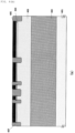
- FIG. 1 is views illustrating an outline structure of a photo detection device 10 according to an embodiment of the present invention, (a) is a plan view, and (b) is a cross-sectional view.
- CMOS transistor circuit 4 comprising a Row control circuit 4-1, a Column control circuit 4-2 that drive these pixels 2, and a signal processing circuit 4-3 etc.
- a thin film silicon (Si) layer on a surface of the silicon chip 1 is divided into a first region and a second region by a shallow trench isolation (STI) as explained in detail below, the pixels 2 arranged in an array are formed in the first region, and the CMOS transistor circuit 4 is formed in the second region.
- STI shallow trench isolation
- the respective pixels 2, the pixels 2 and the Row control circuit 4-1, and the pixels 2 and the Column control circuit 4-2 are connected by metal wires 3.
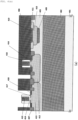
- FIG. 2 is a schematic cross-sectional view illustrating details of the cross-sectional structure illustrated in FIG. 1(b) .
- the photo detection device forms a photodiode (SPAD) 202 that detects an infrared single photon and a CMOS transistor circuit 201 that amplifies and processes a signal from the photodiode 202 by using a wafer in which a P-type doped P-type germanium epitaxial layer 102 is sandwiched by a P-type doped silicon substrate 101 and a P-type thin film silicon layer 103 as a raw material for a wafer process, and performing ion implantation and thermal treatment.
- a photodiode (SPAD) 202 that detects an infrared single photon
- a CMOS transistor circuit 201 that amplifies and processes a signal from the photodiode 202 by using a wafer in which a P-type doped P-type germanium epitaxial layer 102 is sandwiched by a P-type doped silicon substrate 101 and a P-type thin film silicon layer 103 as a raw material for a wafer process,
- FIG. 2 illustrates by an example only one CMOS transistor circuit 201 and one photodiode (SPAD) 202
- the photo detection device in fact, as illustrated in FIG. 1 , comprises multiple SPADs 202 arranged in an array and a CMOS transistor circuitry for driving the SPADs 202 with multiple CMOS transistor circuits 201 combined.
- all-in-one photo detection device capable of detecting an infrared single photon is realized including an amplifier capable of signal amplification and the CMOS transistor circuit 201 capable of signal processing.
- the photodiode (SPAD) 202 is formed on the P-type silicon substrate 101, and the P-type silicon substrate 101 is a general purpose silicon wafer, doped with group III impurity such as boron, and its carrier concentration is 1 ⁇ 10 15 cm -3 to 1 ⁇ 10 19 cm -3 , desirably 1 ⁇ 10 18 cm -3 .
- the P-type germanium epitaxial layer 102 is a layer formed by epitaxial growth on the silicon substrate 101 and P-type doped, and its concentration is 1 ⁇ 10 15 cm -3 to 1 ⁇ 10 16 cm -3 , desirably 7 ⁇ 10 15 cm -3 and a thickness is 4 ⁇ m to 7 ⁇ m, desirably 5.5 ⁇ m.
- the P-type thin film silicon layer 103 is formed whose concentration is 1 ⁇ 10 15 cm -3 to 1 ⁇ 10 16 cm -3 , desirably 7 ⁇ 10 15 cm -3 and whose thickness is 0.8 um to 1.2 ⁇ m, desirably 1.0 um.
- This P-type thin film silicon layer 103 is bonded to the P-type germanium epitaxial layer 102 in room temperature vacuum by surface activated bonding.
- the P-type thin film silicon layer 103 is realized with a thin and uniform film thickness by smart-cut technique using hydrogen ion implantation.
- an APD P-well layer 105, an APD N-well layer 106, and N + diffusion layer 108 are formed by normal ion implantation technique, and a guard ring N-well layer 107 is arranged so as to surround the N + diffusion layer 108.
- the APD P-well layer 105 is a P-type diffusion layer that is located at a depth of 0.7 um to 0.8 um from a surface of the P-type thin film silicon layer 103 and whose concentration is 1 ⁇ 10 16 cm -3 to 1 ⁇ 10 17 cm -3 , desirably 7 ⁇ 10 16 cm -3 , and this layer controls to reduce an electric field at a junction between the P-type thin film silicon layer 103 and the P-type germanium epitaxial layer 102, to thereby reduce a dark current generated at this interface.
- the APD N-well layer 106 is a N-type diffusion layer that is located at a depth of 0.2 um to 0.7 ⁇ m from the surface of the P-type thin film silicon layer 103 and whose concentration is 1 ⁇ 10 15 cm -3 to 1 ⁇ 10 16 cm -3 , desirably 7 ⁇ 10 15 cm -3 .
- the APD P-well layer 105 and the APD N-well layer 106 form together a PN junction, and a high electric field enough to enable avalanche amplification is applied to this junction part.
- the N + diffusion layer 108 whose concentration is 1 ⁇ 10 19 cm -3 to 1 ⁇ 10 21 cm -3 is formed at a depth of 0.2 ⁇ m from the surface of the P-type thin film silicon layer 103.
- This N + diffusion layer 108 may be formed at the same time as an N + diffusion layer 108 that is used in the CMOS transistor circuit 201 part as mentioned below.
- the guard ring N-well layer 107 whose concentration is 1 ⁇ 10 17 cm -3 to 1 ⁇ 10 19 cm -3 is arranged in order to prevent edge breakdown.
- an STI (Shallow Trench Isolation) layer 104 is put in order to perform electrical separation.
- the CMOS transistor circuit 201 is basically made in the P-type thin film silicon layer 103 by existing CMOS manufacturing technology.
- N + diffusion layer 108 and P + diffusion layer 109 that are highly concentrated diffusion layers and constitute a source and drain are arranged.
- the N + diffusion layer 108 and the P + diffusion layer 109 also serve as well contacts connecting to the well layers 110 and 111 with low resistance.
- a gate electrode of a MOSFET is 112
- each electrode of the transistor is connected by an electrode plug 114
- a circuit configuration of the photo detection device is made by metal wires 115.
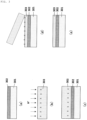
- FIG. 3 illustrates a method of manufacturing a wafer that is a basic material for manufacturing a photo detection device capable of detecting an infrared single photon according to the present invention.
- a P-type germanium epitaxial layer 302 is formed by epitaxial growth.
- a carrier concentration of the P-type germanium epitaxial layer 302 is 1 ⁇ 10 15 cm -3 to 1 ⁇ 10 16 cm -3 , desirably 7 ⁇ 10 15 cm -3 and a thickness is 4 ⁇ m to 7 um, desirably 5.5 ⁇ m.
- H + hydrogen ions
- These two substrates 301 and 303 are bonded together in a vacuum by surface activated bonding technique as illustrated in FIG. 3(c) .
- surface activated bonding two substrates are introduced into a vacuum chamber not shown and each surface thereof is sputtered by Ar ions, and then the two substrates are mechanically bonded together by joining each surface together and applying a pressure of about 300 N for about 60 seconds.
- cleavage occurs in a hydrogen ion implanted region as illustrated in FIG. 3(d) and thus a P-type silicon layer 303 of about 1 ⁇ m can be formed on the P-type germanium epitaxial layer 302.
- CMP chemical mechanical polishing
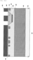
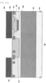
- FIG. 4 is outline cross-sectional views illustrating a wafer process for a photo detection device capable of detecting an infrared single photon.
- a wafer with germanium 402 sandwiched between silicons 401 and 403 is used as a starting material.
- a pad oxide film 404 of 10 to 30 nm is grown by thermal oxidation.
- a silicon nitride film 405 of about 100 to 200 nm is deposited by a low-pressure CVD method.
- a structure of FIG. 4(a) is obtained by patterning the silicon nitride film 405 and the pad oxide film 404 by existing photolithography technique and etching using a photoresist 406 as a mask.
- a shallow trench is formed in the silicon film 403.
- a silicon oxide film of 10 to 20 nm is formed on a trench surface by thermal oxidation.
- CMP chemical mechanical polishing
- the height of the STI oxide film is adjusted to the silicon surface. Furthermore, a structure shown in FIG. 4(c) is obtained by applying 10 to 20 nm sacrificial oxidation by thermal oxidation. The steps up to this point conform to a normal CMOS LOGIC process. Followings will be additional steps specific to the photo detection device capable of detecting an infrared single photon.
- boron ions are implanted by a dose amount of 6 ⁇ 10 11 cm -3 , with an acceleration energy of 310 keV ( FIG. 4(d) ). After that, the photoresist 406 is removed.
- phosphorus ions are implanted by a dose amount of 7 ⁇ 10 11 cm -3 , with an acceleration energy of 330 keV and by a dose amount of 2 ⁇ 10 15 cm -3 , with an acceleration energy of 90 keV ( FIG. 4(e) ). After that, the photoresist 406 is removed.
- phosphorus ions are implanted by a dose amount of 4 ⁇ 10 11 cm -3 , with an acceleration energy of 70 keV and by a dose amount of 4 ⁇ 10 11 cm -3 , with an acceleration energy of 200 keV ( FIG. 4(f) ). After that, the photoresist 406 is removed.
- the steps from the APD P-well photolithography step to this step are additional ones to a normal CMOS LOGIC process, which are necessary for manufacturing the photo detection device capable of detecting an infrared single photon. Since steps after this step will conform to the normal CMOS LOGIC process, detailed conditions thereof are omitted.
- a Logic P-well layer 412 is formed ( FIG. 4(g) ) .
- This step also includes boron or BF2 ion implantation to adjust a threshold of the N-channel transistor. After the ion implantation, the photoresist 406 is removed.
- a Logic N-well layer 413 is formed ( FIG. 4(h) ) .
- This step also includes phosphorus ion implantation to adjust a threshold of the P-channel transistor. After the ion implantation, the photoresist 406 is removed.
- a sacrificial oxide film 408 is removed by hydrofluoric acid etc.
- a gate oxide film 414 is formed by thermal oxidation.
- a polysilicon, which is to be a gate electrode 415, is deposited by low-pressure CVD, the gate electrode 415 is patterned and the photoresist 406 is removed by normal photolithography technique and etching technique, to obtain a structure of FIG. 4(i) .
- n - part 416 for drain electric field relaxation and suppression of short-channel effect of the N-channel transistor after a pattern in which the photoresist 406 of the N-channel transistor part is opened, is formed by normal photolithography technique as illustrated in FIG. 4(j) , arsenic ion implantation to form an LDD (Lightly Doped Drain) for drain electric field relaxation and boron or BF2 ion implantation to make a pocket for mitigation of short-channel effect are performed and the photoresist 406 is removed.
- LDD Lightly Doped Drain
- a p - part 417 as illustrated in FIG. 4(k) , after a pattern in which the photoresist 406 of the P-channel transistor part is opened, is formed, BF2 ion implantation as an LDD and phosphorus ion implantation as a pocket are performed and the photoresist 406 is removed. After that, a silicon oxide film is formed by a CVD method, and a sidewall spacer 418 is formed on a sidewall of the gate electrode 415 by anisotropic etching as illustrated in FIG. 4(l) .
- a photoresist 406 pattern in which the N-channel transistor part is opened is formed as illustrated in FIG. 4(m) .
- photoresist opening is also made in the upper part of APD.
- Arsenic ion implantation using this photoresist 406 as a mask forms a source and drain of the N-channel transistor and the N + diffusion layer 419 of APD.
- a photoresist 406 pattern in which the P-channel transistor part is opened is formed as illustrated in FIG. 4(n) , BF2 ion implantation is performed using this photoresist 406 as a mask, and the photoresist 406 is removed. Furthermore, a silicon oxide film is formed over the entire surface by CVD method etc. and patterning is performed so that silicon oxide film 422 is left on a region on which silicide is not desired to be formed in a subsequent salicide step for resistance reduction.
- the region on which silicide is not desired to be formed is in particular APD part in the present invention, it is configured, as illustrated in FIG. 4(o) , such that silicide is formed on a part on which a contact is to be formed later even on APD part.
- cobalt etc. is spattered, the cobalt is reacted with silicon at a relatively low temperature of about 500 °C, and untreated cobalt on the silicon oxide film is removed by selective etching. Furthermore, applying thermal treatment promotes silicidation and makes a low resistance salicide layer.
- a structure of FIG. 4(p) is obtained by formation of an existing interlayer insulation film 423, formation of a contact and a tungsten plug 424 in the contact, and formation of a first wiring layer 425.
- a multi-layer metal wiring structure is obtained by formation of a metal interlayer film, a via hole, and an upper metal wiring layer.
- a protective film for chip protection is formed on the uppermost metal layer and the protective film on a pad is removed for electrical conduction
- a wafer process for the photo detection device of the present invention is completed by performing backgrinding for making a wafer into a desired thickness, performing backside implantation of boron for lowering the resistance of the backside to form a backside P + diffusion layer.
- the P-type thin film silicon layer 103 is formed by surface activated bonding technique and smart-cut technique using hydrogen ion implantation as illustrated in FIG. 3
- the present invention is not limited thereto, and it may be formed by a method of epitaxially growing silicon of about 1 um on the P-type germanium epitaxial layer 102.
- FIG. 5 illustrates a carrier concentration profile obtained by a process simulation of a main part of the APD that is formed by the above process.
- the horizontal axis designates a depth from the silicon film 403 surface, and the vertical axis designates concentration in the diffusion layer. It is found that the structure illustrated in FIG. 2 is substantially realized by the manufacturing method of the present invention.
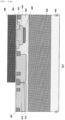
- a method of illuminating a SPAD in order to detect an incident light from an object includes a front surface illumination and a back surface illumination.
- an N + junction 108 on the front side is as thin as 0.5 ⁇ m and there is a depletion layer in which a photoelectric effect occurs, in the P-type germanium epitaxial layer 102 under the junction.
- the P-type thin film silicon layer 103 absorbs a visible light, it is difficult for the thickness of 0.5 ⁇ m to absorb all visible light. Therefore, in the case of the front surface illumination, a visible light shielding filter 120 for shielding a visible light is needed.
- the P-type germanium epitaxial layer 102 is as thin as about 5 ⁇ m, and the P-type silicon substrate 101 thereunder has to have the thickness of at least 200 um for assuring mechanical strength of the chip. Without having to provide a visible light shielding filter on the back surface, a visible light is absorbed by this thick P-type silicon substrate and does not reach the depletion layer formed in the P-type germanium epitaxial layer 102.
- an infrared light whose wavelength is about 1.1 um passes through the silicon (Si) and reaches the depletion layer. Therefore, an SPAD that selectively detects an infrared light only without a visible light shielding filter, can be realized. Therefore, it becomes possible to simplify the steps and reduce the cost because the step of making a filter is unnecessary.
Landscapes
- Light Receiving Elements (AREA)
- Solid State Image Pick-Up Elements (AREA)
- Measuring Pulse, Heart Rate, Blood Pressure Or Blood Flow (AREA)
- Basic Packing Technique (AREA)
Applications Claiming Priority (1)
| Application Number | Priority Date | Filing Date | Title |
|---|---|---|---|
| PCT/JP2022/011878 WO2023175762A1 (ja) | 2022-03-16 | 2022-03-16 | 光検出装置 |
Publications (3)
| Publication Number | Publication Date |
|---|---|
| EP4496010A1 true EP4496010A1 (de) | 2025-01-22 |
| EP4496010A4 EP4496010A4 (de) | 2025-12-10 |
| EP4496010B1 EP4496010B1 (de) | 2026-05-06 |
Family
ID=82320508
Family Applications (1)
| Application Number | Title | Priority Date | Filing Date |
|---|---|---|---|
| EP22769065.8A Active EP4496010B1 (de) | 2022-03-16 | 2022-03-16 | Lichtdetektionsvorrichtung |
Country Status (6)
| Country | Link |
|---|---|
| US (1) | US12396275B2 (de) |
| EP (1) | EP4496010B1 (de) |
| JP (1) | JP7097137B1 (de) |
| CN (1) | CN117083724A (de) |
| TW (1) | TWI813464B (de) |
| WO (1) | WO2023175762A1 (de) |
Families Citing this family (1)
| Publication number | Priority date | Publication date | Assignee | Title |
|---|---|---|---|---|
| CN119300487B (zh) * | 2024-09-30 | 2025-09-23 | 浙江大学 | 一种Pocket掺杂的4H-SiC基雪崩光电二极管器件 |
Family Cites Families (7)
| Publication number | Priority date | Publication date | Assignee | Title |
|---|---|---|---|---|
| ATE401666T1 (de) * | 2002-09-19 | 2008-08-15 | Quantum Semiconductor Llc | Licht-detektierende vorrichtung |
| US20060157806A1 (en) * | 2005-01-18 | 2006-07-20 | Omnivision Technologies, Inc. | Multilayered semiconductor susbtrate and image sensor formed thereon for improved infrared response |
| CN109964315A (zh) * | 2016-08-31 | 2019-07-02 | G射线瑞士公司 | 包括跨越键合界面的电荷输送的电磁辐射检测器 |
| WO2018158631A1 (en) | 2017-03-01 | 2018-09-07 | G-Ray Switzerland Sa | Electromagnetic radiation detector based on wafer bonding |
| US10205037B2 (en) | 2017-06-09 | 2019-02-12 | Taiwan Semiconductor Manufacturing Company Ltd. | Photodiode device and manufacturing method thereof |
| JP2021027358A (ja) * | 2019-08-01 | 2021-02-22 | ダブリュアンドダブリュセンス デバイシーズ, インコーポレイテッドW&Wsens Devices, Inc. | マイクロストラクチャ向上型吸収感光装置 |
| JP2021150359A (ja) | 2020-03-17 | 2021-09-27 | 株式会社東芝 | 光検出素子、光検出システム、ライダー装置、および移動体 |
-
2022
- 2022-03-16 CN CN202280003572.8A patent/CN117083724A/zh active Pending
- 2022-03-16 JP JP2022517402A patent/JP7097137B1/ja active Active
- 2022-03-16 EP EP22769065.8A patent/EP4496010B1/de active Active
- 2022-03-16 US US17/918,111 patent/US12396275B2/en active Active
- 2022-03-16 WO PCT/JP2022/011878 patent/WO2023175762A1/ja not_active Ceased
- 2022-10-07 TW TW111138124A patent/TWI813464B/zh active
Also Published As
| Publication number | Publication date |
|---|---|
| US20240145519A1 (en) | 2024-05-02 |
| JPWO2023175762A1 (de) | 2023-09-21 |
| CN117083724A (zh) | 2023-11-17 |
| WO2023175762A1 (ja) | 2023-09-21 |
| TWI813464B (zh) | 2023-08-21 |
| EP4496010A4 (de) | 2025-12-10 |
| JP7097137B1 (ja) | 2022-07-07 |
| EP4496010B1 (de) | 2026-05-06 |
| TW202339296A (zh) | 2023-10-01 |
| US12396275B2 (en) | 2025-08-19 |
Similar Documents
| Publication | Publication Date | Title |
|---|---|---|
| TWI722060B (zh) | 堆疊式單光子雪崩二極體影像感測器及其形成方法 | |
| KR101485653B1 (ko) | Cmos 이미지 센서 및 이의 형성 방법 | |
| US7651880B2 (en) | Ge short wavelength infrared imager | |
| KR101849494B1 (ko) | 에피텍셜 격리 특징부를 갖는 이미지 센서 디바이스 및 이의 형성 방법 | |
| KR102175615B1 (ko) | 얕은 트렌지 가장자리 도핑을 갖는 cmos 이미지 센서 | |
| US7999292B2 (en) | Image sensor and manufacturing method thereof | |
| US9437644B2 (en) | Semiconductor device and method of manufacturing same | |
| US9786806B2 (en) | Semiconductor device and method for manufacturing the same | |
| US10115751B2 (en) | Semiconductor device | |
| US12132066B2 (en) | Capping structure along image sensor element to mitigate damage to active layer | |
| US20130320419A1 (en) | CIS Image Sensors with Epitaxy Layers and Methods for Forming the Same | |
| US9318630B2 (en) | Pixel with raised photodiode structure | |
| EP4496010B1 (de) | Lichtdetektionsvorrichtung | |
| TWI548074B (zh) | 影像感測元件及其形成方法 | |
| US20150364517A1 (en) | Method of manufacturing solid-state image sensor and solid-state image sensor | |
| US8748955B2 (en) | CMOS image sensor and method for fabricating the same | |
| US10157950B2 (en) | Pixel with spacer layer covering photodiode | |
| TW201735120A (zh) | 半導體裝置及半導體裝置的製造方法 | |
| CN114613795B (zh) | 用于红外图像传感器的新型像素结构及制作方法 | |
| TW202306187A (zh) | 集成晶片結構及其形成方法 | |
| US20150084152A1 (en) | Photodiode |
Legal Events
| Date | Code | Title | Description |
|---|---|---|---|
| STAA | Information on the status of an ep patent application or granted ep patent |
Free format text: STATUS: UNKNOWN |
|
| STAA | Information on the status of an ep patent application or granted ep patent |
Free format text: STATUS: THE INTERNATIONAL PUBLICATION HAS BEEN MADE |
|
| PUAI | Public reference made under article 153(3) epc to a published international application that has entered the european phase |
Free format text: ORIGINAL CODE: 0009012 |
|
| STAA | Information on the status of an ep patent application or granted ep patent |
Free format text: STATUS: REQUEST FOR EXAMINATION WAS MADE |
|
| 17P | Request for examination filed |
Effective date: 20220921 |
|
| AK | Designated contracting states |
Kind code of ref document: A1 Designated state(s): AL AT BE BG CH CY CZ DE DK EE ES FI FR GB GR HR HU IE IS IT LI LT LU LV MC MK MT NL NO PL PT RO RS SE SI SK SM TR |
|
| P01 | Opt-out of the competence of the unified patent court (upc) registered |
Free format text: CASE NUMBER: APP_5016/2025 Effective date: 20250130 |
|
| DAV | Request for validation of the european patent (deleted) | ||
| DAX | Request for extension of the european patent (deleted) | ||
| REG | Reference to a national code |
Ref country code: DE Ref legal event code: R079 Free format text: PREVIOUS MAIN CLASS: H01L0031107000 Ipc: H10F0039000000 Ref country code: DE Ref legal event code: R079 Ref document number: 602022036363 Country of ref document: DE Free format text: PREVIOUS MAIN CLASS: H01L0031107000 Ipc: H10F0039000000 |
|
| A4 | Supplementary search report drawn up and despatched |
Effective date: 20251106 |
|
| RIC1 | Information provided on ipc code assigned before grant |
Ipc: H10F 39/00 20250101AFI20251031BHEP Ipc: H10F 39/12 20250101ALI20251031BHEP Ipc: H10F 39/18 20250101ALI20251031BHEP Ipc: H10F 30/20 20250101ALI20251031BHEP |
|
| GRAP | Despatch of communication of intention to grant a patent |
Free format text: ORIGINAL CODE: EPIDOSNIGR1 |
|
| STAA | Information on the status of an ep patent application or granted ep patent |
Free format text: STATUS: GRANT OF PATENT IS INTENDED |
|
| RIC1 | Information provided on ipc code assigned before grant |
Ipc: H10F 39/00 20250101AFI20251204BHEP Ipc: H10F 39/12 20250101ALI20251204BHEP Ipc: H10F 39/18 20250101ALI20251204BHEP Ipc: H10F 30/20 20250101ALI20251204BHEP |
|
| INTG | Intention to grant announced |
Effective date: 20251223 |
|
| GRAS | Grant fee paid |
Free format text: ORIGINAL CODE: EPIDOSNIGR3 |
|
| GRAA | (expected) grant |
Free format text: ORIGINAL CODE: 0009210 |
|
| STAA | Information on the status of an ep patent application or granted ep patent |
Free format text: STATUS: THE PATENT HAS BEEN GRANTED |