EP4496335A1 - Capteur d'image et procédé de fabrication d'un capteur d'image - Google Patents
Capteur d'image et procédé de fabrication d'un capteur d'image Download PDFInfo
- Publication number
- EP4496335A1 EP4496335A1 EP23185791.3A EP23185791A EP4496335A1 EP 4496335 A1 EP4496335 A1 EP 4496335A1 EP 23185791 A EP23185791 A EP 23185791A EP 4496335 A1 EP4496335 A1 EP 4496335A1
- Authority
- EP
- European Patent Office
- Prior art keywords
- bit
- output
- codes
- detector elements
- image sensor
- Prior art date
- Legal status (The legal status is an assumption and is not a legal conclusion. Google has not performed a legal analysis and makes no representation as to the accuracy of the status listed.)
- Granted
Links
Images




Classifications
-
- H—ELECTRICITY
- H04—ELECTRIC COMMUNICATION TECHNIQUE
- H04N—PICTORIAL COMMUNICATION, e.g. TELEVISION
- H04N25/00—Circuitry of solid-state image sensors [SSIS]; Control thereof
- H04N25/70—SSIS architectures; Circuits associated therewith
- H04N25/76—Addressed sensors, e.g. MOS or CMOS sensors
- H04N25/78—Readout circuits for addressed sensors, e.g. output amplifiers or A/D converters
-
- H—ELECTRICITY
- H04—ELECTRIC COMMUNICATION TECHNIQUE
- H04N—PICTORIAL COMMUNICATION, e.g. TELEVISION
- H04N25/00—Circuitry of solid-state image sensors [SSIS]; Control thereof
- H04N25/70—SSIS architectures; Circuits associated therewith
- H04N25/76—Addressed sensors, e.g. MOS or CMOS sensors
-
- H—ELECTRICITY
- H04—ELECTRIC COMMUNICATION TECHNIQUE
- H04N—PICTORIAL COMMUNICATION, e.g. TELEVISION
- H04N25/00—Circuitry of solid-state image sensors [SSIS]; Control thereof
- H04N25/70—SSIS architectures; Circuits associated therewith
- H04N25/76—Addressed sensors, e.g. MOS or CMOS sensors
- H04N25/77—Pixel circuitry, e.g. memories, A/D converters, pixel amplifiers, shared circuits or shared components
- H04N25/772—Pixel circuitry, e.g. memories, A/D converters, pixel amplifiers, shared circuits or shared components comprising A/D, V/T, V/F, I/T or I/F converters
- H04N25/773—Pixel circuitry, e.g. memories, A/D converters, pixel amplifiers, shared circuits or shared components comprising A/D, V/T, V/F, I/T or I/F converters comprising photon counting circuits, e.g. single photon detection [SPD] or single photon avalanche diodes [SPAD]
Definitions
- the present disclosure relates to an image sensor comprising a plurality of detector elements, such as photon-counting detector elements, and a method of producing an image sensor. More particularly, the disclosure concerns SPAD sensors (SPAD: Single-Photon Avalanche Diodes) in which the most common problems in SoC design (SoC: system on a chip) for SPAD sensors are mitigated, namely jitter, noise and/or power and ground bouncing.
- SPAD sensors Single-Photon Avalanche Diodes
- SPAD image sensors usually have SPAD arrays connected to electronics that process the timing and intensity information of the detected photons to transmit the results to an external system.
- SPAD sensors are for example described in WO 2020 / 151 838 A1 and WO 2020 / 207 571 A1 .
- the external communication of a SPAD sensor is one of the parts of the overall system that consumes the most power.
- Input and Output cells use a relatively higher voltage than the core; additionally, the capacitances that the IO cells have to charge and discharge in every cycle are also much higher. Consequently, the IO banks consume considerable power.
- the current peaks generated during the transmission from the IO cells are supplied through inductors that, problematically, generate ground and power bouncing effects.
- some systems use a differential approach such as LVDS (Low Voltage Differential Signaling), USB (Universal Serial Bus), and different Ethernet standards.
- SE Single-Ended
- an electrical signal is transmitted using one wire which carries a varying (high/low) voltage that represents the signal.
- Another wire may be used and connected to a reference voltage, usually ground.
- a reference voltage usually ground.
- one conductor for each signal can be used and additionally one shared ground connection or several non-shared ground connections can be provided. If the single-ended approach is used, ground and power bouncing effects remain a problem at interfaces between different voltage domains.
- FIG. 1 shows an interface between two different voltage domains VD1 and VD2 for Single-Ended (SE) operation.
- a dashed line SEP represents the separation of the domains VD1 and VD2.
- the voltage domain VD1 comprises a P-MOS transistor MP 1 , an N-MOS transistor MN 1 and inductors L 1 and L 2 .
- L 1 connects to the source of MP 1 whereas L 2 is connected at the source of N-MOS transistor MN 1 .
- voltage domain VD 2 comprises a P-MOS transistor MP 2 , an N-MOS transistor MN 2 and inductors L 3 and L 4 .
- L 2 is connected at the source of MP 3 and L 4 is connected at the source of MN 2 .
- the drain of MP 1 , the gate of MP 2 , the gate of MN 2 and the drain of MN 1 are connected with each other.
- the drawing further indicates the voltages Vc ore and Vs at the source of MP 1 and MP 2 respectively; the voltages Vss core and Vss s at the source of the N-MOS transistors MN 1 and MN 2 , respectively, and Vss.
- Document [1] describes that 8-bit words are mapped on 10-bit symbols to achieve DC balance, i.e., a balanced signal strength averaged over a time interval.
- DC balance i.e., a balanced signal strength averaged over a time interval.
- the difference between the counts of ones and zeros in a string of bits (a sequence of symbols) shall not exceed a predefined threshold.
- enough state changes shall be provided to allow reasonable clock recovery which is achieved by not providing more than five ones or zeros in a row.
- Documents [2] to [5] describe SPAD sensors. Reducing the skew in the output tracks of the SPAD may be accomplished by OR-ing the outputs in a sectional way (document [2]) or in an H-tree fashion (document [3]). However, the result of these methods is a fixed connection of the SPAD outputs that cannot be changed at run-time. Other systems keep track on the address of the SPADs that fired, either by propagating the address of the first SPAD that fired (document [4]) or noting the codes of the SPADs that fired and dismissing the collisions (document [5]).
- An image sensor of an embodiment of the invention includes detector elements and at least one electronic module which is connected with the detector elements and which is configured to output n-bit output words, wherein at least some of the n-bit output words include measurement data from the detector elements.
- the image sensor further comprises an n-bit to m-bit converter which converts each of the n-bit output words to an m-bit code, where m is larger than n (or m ⁇ n +1).
- the n-bit to m-bit converter uses only a subset of all possible m-bit codes to encode the n-bit output words.
- the subset is chosen such that a difference between a number (i.e., amount) of zeros and ones of each m-bit code in the subset is on average smaller than an average difference between a number of zeros and ones of all possible n-bit output words.
- the image sensor further comprises an output unit (in particular for single-ended communication and) configured to output the m-bit code.
- the image sensor includes detector elements and an electronic module configured to output n-bit output words, at least some of which include measurement data from the detector elements .
- the image sensor is provided with an n-bit to m-bit converter which converts each of the n-bit output words to an m-bit code, where m is larger than n.
- the image sensor is further provided with an output unit configured for outputting the m-bit code, in particular by single-ended communication.
- the n-bit to m-bit converter uses only a subset of all possible m-bit codes to encode the n-bit output words, wherein the subset is chosen such that a difference between a number of zeros and ones of each m-bit code in the subset is on average smaller than an average difference between a number of zeros and ones of all possible n-bit output words.
- a digital communication module can thus have single-ended outputs which are substantially balanced in terms of the number of high and low signal levels (1 and 0), at least while measurement data from the detector elements is output. Input currents and output currents of an integrated circuit which forms the image sensor are substantially equalized.
- the above-mentioned difference between a number (i.e., amount) of zeros and ones of each m-bit code shall mean that the number of ones in the m-bit code is counted and similarly the number of zeros in this code is counted, then the difference between these two numbers is built.
- the average difference between zeros and ones of all possible n-bit output words can be understood such that the number of zeros and the number of ones in one n-bit output word are counted, the difference between these two numbers is calculated; such a difference is built for each possible n-bit output word, and finally the average of all these differences is calculated.
- the difference for the m-bit codes of the subset is on average smaller than the average difference of all n-bit output words, i.e., while in principle some differences for m-bit codes of the subset may be larger than the average difference for all n-bit output words, the average of all differences for m-bit codes of the subset is lower. More particularly, the subset may be chosen such that for all m-bit codes of the subset, the difference between the number of zeros and ones may be smaller than the average difference between zeros and ones of all possible n-bit output words.
- the absolute values may be used, i.e., the difference for a code including six 1s and three 0s is the same as the difference for a code including three 1s and six 0s.
- n-bit output words of a non-inventive SPAD sensor are output via its single-ended input/output cell, wherein the full range of possible n-bit output words is used.
- the transition from one output word to the next can have up to n transitions between the number of ones and zeros in the code.
- the transition from the 9-bit output word 110111011 to a next 9-bit output word 010000100 has six negative changes from 1 to 0 and one positive change from 0 to 1, resulting in a sum of five negative changes.
- the ground and power bouncing effect is particularly pronounced and affects considerably the conventional SPAD system.
- the invention reduces on average the number of changes between the sum of ones or zeros of the codes that are actually output. Ground and power bouncing effects are favourably reduced.
- the n-bit output words (which may include any possible codes and thus up to n changes between zeros and ones of two n-bit output words) are not themselves output but rather these n-bit output words are converted to m-bit codes which are then output. Not all 2 ⁇ m possible m-bit codes are used. Instead only a subset with preferably an equalized number of zeros and ones of each m-bit code is used.
- the subset of used 11-bit codes may be limited to 11-bit codes that include five or six ones (and thus six or five zeros).
- the transition from one 11-bit code to the next 11-bit code can thus have a change in the difference between ones and zeros of just minus one, zero, or plus one.
- This exemplary subset rules out that the summed number of changes is larger than one, and hence bouncing and noise is significantly reduced.
- the detector elements may be photon-counting detector elements such as SPAD elements which, e.g., output one pulse per registered photon.
- the detector elements may also be configured to output a signal (e.g., voltage or current) with a strength indicative of an intensity of light impinging on the respective detector element.
- a signal e.g., voltage or current
- several exemplary embodiments refer to SPAD sensors or photon-counting detector elements; however, the described features may be equally used in other image sensors which use detector elements differing from photon-counting detector elements or SPADs.
- the image sensor may in particular be used for applications in which accurate counting of single photons and/or timing information is crucial, e.g., for microscopes, LiDAR systems (LiDAR: light detection and ranging) or PET systems (PET: position emission tomography).
- Exemplary embodiments may thus also comprise a light microscope or LiDAR or PET system with an image sensor formed as described herein.
- the measurement data included in n-bit output words may include any (processed) data stemming from the detector elements, i.e., the raw signals output by the detector elements may be further processed, in particular by the electronic module, and the processed data is output.
- the measurement data may include count values indicative of numbers of photons registered with the detector elements and/or timing information on registered photons.
- the electronic module may be configured to process raw measurement signals from the detector elements to generate timing information and/or the electronic module may include at least one counter configured to count photons registered with one or more of the photon-counting detector elements.
- the output unit of the SPAD sensor may be configured for single-ended communication. It may comprise several (in particular a number of m or at least m) (input/output cells forming a bus for outputting the m-bit code. Each cell comprises a pad which outputs one bit of the m-bit code. The individual bits of the m-bit code are thus not output one after the other, but simultaneously in parallel.
- a high or low level is output at a pad depending on whether a one or zero shall be output.
- Each pad may serve to output the information of one bit of the m-bit codes.
- a constant reference voltage e.g., ground, is provided with regard to which the voltage levels at the pads are determined.
- a common ground may be used for all pads.
- the output unit may be formed in a distributed manner in which its components are not directly adjacent each other.
- the output unit may also be referred to as an input/output unit which comprises one or more electrical contacts for, e.g., power supply and/or receiving information.
- the same contacts, e.g., pads may be used for outputting data and for receiving data.
- the ones and zeros of an m-bit code are simultaneously output in parallel.
- the equalization of ones and zeros within an m-bit code has the effect that the ones and zeros that are output at the same time are equalized.
- the ones and zeros that are output are equalized and consequently the input and output currents at the bus are equalized.
- Equalized ones and zeros may mean equal numbers of ones and zeros in an m-bit code. More generally, equalized ones and zeros may mean that a difference between the number of ones and the number of zeros is smaller than n/2 or n/3, n being the number of bits of the original n-bit output words.
- the n-bit to m-bit converter is included on a common chip of the image sensor. It receives an n-bit output word and converts this n-bit output word to an m-bit code, which is then output by the n-bit to m-bit converter to an output unit of the chip. Every n-bit word is converted to a unique m-bit code such that it is possible to convert the m-bit code back to the n-bit word without ambiguity. Only the m-bit codes but not the n-bit output words are output from the common chip of the image sensor.
- the n-bit to m-bit converter may be an n-bit to m-bit conversion LUT (LUT: look-up table) which can be a hardware component included on a common chip (integrated circuit) of the image sensor / SPAD sensor.
- LUT look-up table
- LUT look-up table
- the number of m is at least one larger than n.
- m may be exactly or at least two or three larger than n.
- the number of all possible m-bit codes is four times the number of all n-bit output words to be encoded, and hence the subset of m-bit codes chosen for encoding the n-bit words may be formed by only the quarter of all possible m-bit codes which has a rather balanced or best balanced/equalized number of ones and zeros.
- a higher bit number is usually not necessary for reaching the intended balance, and hence unduly high bit numbers can be avoided if m exceeds n by not more than three or n/3.
- the difference of ones and zeros of one m-bit code and the difference of ones and zeros of another m-bit code shall, on average, differ less than the differences of ones and zeros of two n-bit output words.
- the difference of ones and zeros of one m-bit code may be understood as the number of ones of this m-bit code minus the number of zeros of this m-bit code. In one example, only m-bit codes with a difference between their numbers of ones and zeros being at most 1 are used to encode n-bit output words.
- the number of m-bit codes included in the subset may be chosen to be 2 ⁇ n or identical to the number of different n-bit output words.
- those 2 ⁇ n different m-bit codes may be chosen for the subset which have a smallest difference in their occurrence of 1s and 0s.
- those m-bit codes which have a highest difference between their numbers of ones and zeros are not included in the subset used for encoding the n-bit output words.
- the m-bit code with only ones, the m-bit code with only zeros, and all m-bit codes with only a single one or a single zero are excluded.
- m-bit codes with only 1s or only 0s are excluded from the subset / not chosen for the subset, and additionally m-bit codes with only one 1 or only one 0 are excluded from the subset if a remaining number of m-bit codes is still ⁇ 2 ⁇ n (i.e., at least as large as the number of possible n-bit output words) and thus sufficient to encode all possible n-bit output words. Furthermore, all m-bit codes with only two 1s or only two 0s are excluded from the subset if a remaining number of m-bit codes is still ⁇ 2 ⁇ n or sufficient to encode all possible n-bit output words.
- the group of m-bit codes may include all m-bit codes with the same number of zeros and ones; additionally the group may include all m-bit codes with a difference between their number of ones and their number of zeros not exceeding 1 (more generally: not exceeding L, where L starts with 1 and is incrementally increased by 1); the process stops if the group of m-bit codes is sufficiently large to encode all n-bit output words. In many cases, this balanced group of m-bit codes is larger than the number of different n-bit words and hence a subset of codes to be used need to be selected from the balanced group of m-bit codes.
- the selection of m-bit codes for the subset is important for reducing the complexity of the hardware components of the n-bit to m-bit conversion LUT, as addressed in the following.
- an n-bit to m-bit conversion LUT may need substantial space when formed in silicon, i.e., an LUT in which the n-bit to m-bit conversion is implemented purely through hardware components, without software performing the n-bit to m-bit conversion.
- a Karnaugh map indicates the intended output for each input. The Karnaugh map is solved for every input-output pair and is used for determining the hardware configuration, in particular to minimize the transistor gate usage. The selection of the subset of m-bit codes affects the complexity of the Karnaugh map and thus the number of required gates or other logic components used in the n-bit to m-bit conversion LUT.
- Minimizing the gate usage also translates into less area required for the n-bit to m-bit conversion LUT and less delay in the conversion process.
- the complexity of the Karnaugh map can be reduced if an m-bit code that is selected to encode an n-bit output word is similar to the n-bit output word. Similarity is understood in this regard as particularly few 0/1 swaps needed so that the sequence of zeros and ones of the n-bit output word is included in the m-bit code. For instance, the sequence of zeros and ones of the n-bit word 111000111 is fully included in the m-bit code 11100011100 and hence the similarly between these two elements is maximal. Selecting such pairs of an n-bit output word and an m-bit code with similar bit sequence ensures that the n-bit to m-bit mapping can be implemented with few hardware components and thus in a compact manner and without significant delay in the processing.
- a mapping between the n-bit output words and the m-bit codes can be constructed / defined through at least the following processes. These processes also determine which m-bit codes are selected to form the previously described subgroup:
- Process C may start with searching the m-bit codes for an m-bit code which requires only one 1/0 swap in its sequence of ones and zeros so that the resulting sequence of ones and zeros includes identically the sequence of ones and zeros of a given n-bit output word. If the search does not yield results, the search is continued for an m-bit code that requires (only) two 1/0 swaps in its sequence to include the sequence of ones and zeros of a given n-bit output word. The search of process C may be performed until a predetermined maximum number of 1/0 swaps is reached.
- Process D The n-bit output word is mapped to an m-bit code which is chosen randomly or according to a predefined order out of the group of balanced codes. Process D thus provides a mapping between two elements of a low similarity.
- process D is only performed after process B has been performed for all n-bit output words and optionally after process C has been performed for all n-bit output words for which no mapping was set in process B. This has the consequence that process D does not block any m-bit codes which may be better suited for other n-bit output words. Process D is thus performed with a reduced group of balanced codes from which many codes have already been assigned through processes B and C.
- process C may optionally only be performed after process B has been performed for all n-bit output words.
- An algorithm may automatically perform the above-described processes to find the best combination possible to generate the conversion LUT.
- the reduction of the complexity of the problem is relevant for achieving the requirements on area and delay.
- a ROM IP may in principle be used for implementing the conversion LUT.
- an ROM IP may complicate satisfying the delay requirements, and it would need more area and incur additional costs.
- the above processes A to D are performed for designing or producing the image sensor.
- the processes A to D result in a mapping which is then built in the n-bit to m-bit conversion LUT and remains fixed.
- the processes A to D are thus not performed during operation of the image sensor.
- An n-bit output word is preferably mapped to an m-bit code including exactly the sequence of bits of the n-bit output word. Therefore, the number of m-bit codes of the subset which include exactly the sequences of their respective n-bit output words is higher than in a theoretical case of an arbitrary mapping between the n-bit output words and the m-bit codes of the subset.
- a positive transition shall be understood as a change from 0 to 1 of a specific bit in the m-bit code, from one code to the next.
- a negative transition indicates a change from 1 to 0 of a specific bit.
- a positive transition of one bit and a negative transition of another bit lead to currents cancelling out each other so that the relevant difference indicates the difference between the number of positive transitions and the number of negative transitions from one code to the next.
- the subset of m-bit codes is chosen such that an average difference in the number of ones between two randomly drawn m-bit codes of the subset is smaller than an average difference (or smaller than 0.5 of the average difference) in the number of ones between two randomly drawn n-bit output words.
- Randomly drawn shall be understood such that two elements out of all possible elements are randomly selected, wherein each element has the same probability to be selected.
- an element is any one of all the n-bit output words
- m-bit codes an element is one of the m-bit codes of the subset.
- the difference in the number of 1s in two m-bit codes of the subset is smaller than the difference in the number of 1s in two n-bit output words.
- Two consecutively output m-bit codes will therefore, on average, have a smaller difference in their numbers of 1s (or zeros) compared with the case that n-bit output words would be output consecutively. Current changes at an output interface of the image sensor chip are thus reduced.
- Parity Bit Optionally, a parity bit can be added to an m-bit code.
- the resulting codes have thus m+1 bits.
- a parity bit serves for error detection.
- the parity bit added to each m-bit code is either 0 or 1 such that the resulting sum of all ones in the m+1 bit code is always odd (or always even).
- the parity bit is thus zero if the number of ones is six.
- the parity bit is consequently one.
- the resulting m+1 bits will always have six ones, in contrast to the m-bit codes which have a varying number of either five or six ones.
- the parity bit serves the usual purpose to detect possible transmission errors: If the received bit sequence does not have an even number of ones, it can be concluded that there has been an error after the m+1 bit code was output by the output cells.
- an error detection and correction becomes possible due to the circumstance that only a subset of all possible m-bit codes is used. If the external system receives an m-bit code which does not match any of the m-bit codes included in the subset, the external system judges the received m-bit code to be erroneous. Optionally, the external system checks whether there is only one possibility to change one bit of the received m-bit code such that an m-bit code included in the subset results. If this is the case, the external system makes this change to generate a corrected m-bit code. This correction is based on the assumption that only one bit (and not more than one bit) is corrupt.
- the described error detection and correction procedure may be performed by software and/or dedicated hardware of the external system.
- n-bit to m-bit converter can also be used in other communication systems in which the n-bit output words are not derived from detector elements or other image sensors but constitute any type of data to be transmitted in single-ended mode.
- Such a communication system comprises an n-bit to m-bit converter (conversion LUT) as described in this disclosure, and an output unit for single-ended communication and configured to output the m-bit code.
- the invention also refers to a SPAD sensor device including an image sensor according to one of the described embodiments of the invention.
- the image sensor / SPAD sensor is formed as a system on a chip.
- the photon-counting detector elements, the electronic module, the n-bit to m-bit conversion LUT and the (input/output unit can all be built on the same chip.
- the n-bit to m-bit conversion is performed on the chip before transmission out of the chip such that the chip outputs are balanced.
- the SPAD sensor device further includes an external electronic system which is not part of said chip.
- the external electronic system shall receive data output from the input/output unit.
- the external electronic system may comprise pins electrically connected with pads of the input/output unit.
- the external electronic system further includes an m-bit to n-bit reverse converter which is arranged to receive m-bit codes output by the input/output unit.
- the m-bit to n-bit reverse converter is thus electrically connected with the input/output unit, e.g., through the mentioned connection between the pins and pads.
- the m-bit to n-bit reverse converter is configured to determine and output the n-bit output words from the m-bit codes.
- the operation of the m-bit to n-bit reverse converter is thus inverse to the operation of the n-bit to m-bit converter .
- the m-bit to n-bit reverse converter may perform the translation to n-bit words as an LUT purely by hardware (similar to the n-bit to m-bit conversion LUT) or a memory (RAM/ROM) that maps the balanced codes into binary codes.
- the n-bit to m-bit reverse converter may also perform the translation through software. This is possible because limitations on used area, power effects and calculation speed are less severe outside the image sensor chip.
- SPADs or photon counting detector elements may be connected directly to input/output (10) cells of the chip. In particular, they may not be pre-processed in any way. These direct connections to the outputs may be provided to preserve the timing information to be processed by an external module.
- the described problem of power and ground bouncing may also occur if many SPADs fire at the same time. This situation is likely for moderate-to-high activity scenarios in which several or all of the SPADs are illuminated simultaneously, in particular in applications such as TCSPC (time-correlated single photon counting). In such a situation, many IO cells will suddenly change their state to 1 and this will create bouncing issues in the power and ground lines.
- two groups of differently configured (photon-counting) detector elements may be provided: At least some of the detector elements belong to a first group of detector elements which are configured to be active-high and are (directly) connected with (input/)output cells, e.g., pads, which correspondingly change to a high state if the detector elements of the first group detect photons. Others of the detector elements belong to a second group of detector elements which are configured to be active-low and are (directly) connected with output cells which change to a low state if the detector elements of the second group detect photons. For example, each detector element of the second group may be provided with an inverter such that its output becomes active-low.
- the detector elements of the first group are not provided with inverters but with buffers.
- Active-high shall be understood such that an output of a detector element is low if no photon is detected and becomes transitorily high upon detection of a photon.
- active-low shall indicate that the output (after the inverter) is high when no photon is registered and becomes low upon detection of a photon.
- high and “low” may be understood such that a voltage of a high state is higher than a voltage of a low state.
- outputs of some of the (photon-counting) detector elements may be inverted to be active-low, whereas outputs of other detector elements are not inverted and are active-high. At least a number of the detector elements whose outputs are active-high and a number of the detector elements whose outputs are active-low are connected to output cells without counters (or other components that convert the received signal into a digital n-bit word) being connected in-between.
- the inversion stage is added for a part of the outputs in order to equalize input and output currents of the integrated circuit.
- the provision of the two groups lowers the bouncing effects when many SPADs are firing together as changes in current at the (input/output cells are favorably reduced.
- the first and second groups may include the same number of detector elements or, more generally, their numbers of detector elements may not deviate from each other by more than 20%. In this way, if all detector elements change at the same time from a state of registering no photons to state of registering a photon, a change in current at the IO cells will be comparatively small.
- the buffers and inverters can be placed in a strategic way with the objective of avoiding that particular image patterns activate a large part of the sensor array that belongs to only one of the two groups (with either buffers or inverters).
- the detector elements that are active-high and the detector elements that are active-low may be arranged in an alternating or interleaved manner. In an alternating arrangement, always one active-high detector element may alternate with one active-low detector element within each row and/or column, or a group of active-high detector elements may alternative with a group of active-low detector elements within each row and/or column.
- the first and second groups are evenly mixed such that a detector element that is active-high is arranged between two detector elements that are active-low.
- the alternating arrangement may apply to both columns and rows of detector elements. In many scenarios, neighbouring detector elements are simultaneously illuminated and hence the alternating pattern is particularly useful in achieving a balanced number of high and low outputs at the IO cells.
- an alternating pattern may be defined by describing the sensor array as a matrix with columns and rows, wherein the column number is denoted with i and the row number is denoted with j.
- Grouping detector elements into the first and second groups may concern all detector elements or it may only concern some detector elements which are not connected with a connection matrix and/or one or more counters.
- the inversion stage for one group can also be advantageously used in connection with the connection matrix and counters that output digital count values: If the connection matrix comprises a plurality of outputs that are not led to counters but are instead directly output from the chip (through e.g., pads of IO cells), the inversion stage ensures balanced currents for these direct outputs (which are separate from the counter).
- the digital counter outputs may be processed by the n-bit to m-bit converter to achieve balanced currents.
- the inversion stage and the n-bit to m-bit converter can therefore advantageously complement each other to balance input/output currents and minimize bouncing effects.
- a plurality of (photon-counting) detector elements may be connected with output cells, wherein each output cell outputs a signal when a detector element connected with this output cell registers a photon.
- the number of detector elements may be larger than the number of output cells.
- a connection matrix may be used to (flexibly) combine outputs from several detector elements to a macropixel signal forwarded to one output cell.
- Inverters may be arranged in some but not all of the lines to output cells, in principle anywhere between the detector elements and the output cells. As noted, the inverters generate a high signal at the respective output cell when no photon is registered, and a low signal when a photon is registered. In particular, the inverters may be arranged between the connection matrix and the output cells.
- Half of all output cells may be equipped with an inverter in their line, thus being active low. This ensures better balanced output signals substantially independent of the light intensity on the sensor.
- connection matrix is configured to (optionally flexibly) combine signals from a number of detector elements into one signal (macropixel output) which is forwarded to one of the output cells.
- An inversion is achieved if the connection matrix is configured such that the macropixel output is a low signal when at least one of the number of detector elements detects a photon and outputs a high signal, whereas the macropixel output is a high signal when none of the number of detector elements detects any photon and thus each of the number of detector elements outputs a low signal.
- connection matrix is configured to provide such an inversion only for output lines to some of the output cells, e.g., for 50% of the output cells or more generally for output lines to a number between 30% and 70% of all output cells. Also this design achieves that the outputs of all output cells are better balances irrespective of the intensity of light hitting the sensor.
- the described features of the inversion may apply to any image sensor that includes (photon-counting) detector elements, and which may include an electronic module with at least one counter configured to count photons registered with one or more of the detector elements, the electronic module configured to output n-bit output words which include count values indicative of numbers of registered photons.
- the described n-bit to m-bit converter may be used for this image sensor.
- Each (photon-counting) detector element is connected to an output track (output line) which forwards an output of the respective detector element.
- the generally high number of SPAD elements and the interconnection between the SPAD elements and the electronics easily leads to a skew (difference in the lengths of the output tracks), which worsens the time performance.
- at least some of the output tracks may form wiggles to increase a length of the respective output tracks.
- a wiggle or curl is understood as a deviation from a straight line to increase the length of the line.
- a wiggle may have, for example, a wave or sinusoidal shape, a zigzag (triangle) shape or a square shape (i.e., four right angle bends are introduced into a straight line).
- Each wiggle may contribute the same extra length to the respective output track, however, in general it is also possible to use wiggles with different size.
- a number of wiggles per output track is chosen such that all output tracks have a common length.
- an equalization algorithm may be provided which automatically calculates the number of wiggles (or summed length of all wiggles) that shall be provided per output track such that all output tracks have the same length.
- the equalization algorithm considers the geometry of the space available for the output tracks and wiggles, i.e., the space between the SPAD elements and a connection matrix or monostables which are described in more detail later.
- the wiggles can be provided in a spread or evenly distributed way, thus randomizing the line crosses. This equalizes the parasitics and crosstalk.
- Ground shield lines may be arranged between the output tracks of the detector elements to reduce a coupling effect between the output tracks.
- the ground shield lines and output tracks may in particular alternate such that one ground shield line is always between two neighbouring output tracks.
- Wiggles may also be added to digital communication lines, e.g., through which n-bit output words and/or m-bit codes are transmitted.
- the lengths of lines for transmitting the individual bits of an n-bit output word are thus made equal.
- all lines for transmitting the individual bits of an m-bit code have the same length.
- the described wiggles may in general be provided at output tracks of detector elements of any image sensor, in particular the image sensor described above which includes the n-bit to m-bit converter and/or the inversion stage for direct SPAD outputs.
- the electronic module may include a connection matrix configured to flexibly combine the outputs of any of the (photon-counting) detector elements into one or more combined signals, thus grouping the detector elements to macro-pixels.
- Reconfigurable macro-pixels are formed in that every pixel (photon-counting detector element) of the SPAD array is connected in a reconfigurable scheme with other SPADs.
- the connection matrix may include an OR matrix in which a signal is output if anyone of several inputs of a logical OR unit receives a signal.
- the connection matrix may also include other logical units than OR connections to combine several inputs.
- connection matrix can be configured to flexibly change which outputs are combined at run-time, e.g., using an internal memory. Any arbitrary combination of outputs is possible, to which end the connection matrix may be equipped with SRAM memories and/or LUTs.
- the connection matrix can be flexibly varied to change the number of macro-pixels, and furthermore the number of detector elements to be combined into one macro-pixel can be flexibly set.
- the outputs of the macro-pixels may be connected to outputs of an integrated circuit of the image sensor or may be further processed before being output from the image sensor.
- the connection matrix can also bet set such that the outputs of some detector elements are just forwarded, without being combined with outputs of other detector elements.
- connection matrix requires a high number of lines due to the fully-connected capability of the system. Any difference in length of these lines would create time skew among the SPADs. In particular because the size of the SPAD array is not negligible in terms of distance, there is, without further measures, an inherit skew in the length of these lines that translates into time skew.
- connection matrix combines outputs of a plurality of detector elements, the information from which detector element an output stems (i.e., the address of the firing SPAD element) is lost. Consequently, any skew in the output tracks cannot be corrected after the connection matrix. Uncorrected skew leads to time jitter which deteriorates the overall time precision. The wiggles for avoiding skew are thus added between the detector elements and the connection matrix.
- a monostable circuit may be provided between the photon-counting detector elements and the connection matrix.
- each output tracks of the photon-counting detector elements leads to a monostable and from there to the connection matrix.
- the monostable serves for reducing the pulse duration of a pulsed signal, e.g., the time length of a high state following the registration of a photon by a SPAD element.
- Each monostable thus outputs shortened fixed-length pulses. This is advantageous when the outputs of several SPAD elements are combined by the connection matrix as the signals/outputs need to be timely separated in order to form distinguishable signals in a combined output of the connection matrix.
- the wiggles may be added between the photon counting detector elements and the monostable circuit so that the lengths of the lines up to the monostables are made equal.
- wiggles may be provided after the monostable and optionally also before the monostable so as to equalize the line length from the photon counting detector elements to the connection matrix.
- the described detector elements may be photon-counting detector elements and may form at least one array (sensor array).
- a pixel shall be understood as one element of the sensor or sensor array, i.e., one detector element.
- n-bit output words and m-bit codes For easier understanding, several embodiments are described with reference to a particular bit number of n-bit output words and m-bit codes. However, indicated exemplary bit numbers only serve to facilitate understanding and the described features shall be more generally understood to apply to any n-bit output word and m-bit code, wherein m is larger than n, in particular larger by (at least) two.
- n may be any positive (whole) number
- m may be any positive (whole) number that is larger than n.
- m may be between 1.1 *n and 1.5*n (but at least ⁇ n+1).
- the single-ended communication with m-bit codes is more efficient as long as m ⁇ 2*n.
- the subset of m-bit codes shall be understood such that only some of all possible m-bit codes can be outputs of the n-bit to m-bit converter. "All possible m-bit codes” shall comprise all codes with m bits, irrespective of their sequence of 1s and 0s.
- the n-bit to m-bit converter converts any n-bit output word, wherein all or some of these n-bit output words may indicate count values of photons.
- the conversion to an m-bit code can concern any digital data and is not limited to photon count values.
- other information included in an n-bit output word to be converted to an m-bit code which is then output from the chip may indicate settings of the connection matrix or may include timing information, status information on components of the chip, control commands or warnings / error messages generated by components of the chip.
- one n-bit output word may correspond to one count value.
- one n-bit output word includes more or less information than one count value.
- the frequency of outputting m-bit codes may be at least twice the frequency with which 10-bit count values are generated.
- n can be any number that does not need to be connected to the number of bits of count values.
- the electronic module of the image sensor comprises one or more electronic units which are built on the same chip as the detector elements.
- the electronic module may in particular include at least one connection matrix and/or analog and digital modules for time-resolved detection or photon counting.
- the feature according to which the electronic module outputs n-bit output words may be understood such that the n-bit output words are output to other components of the electronic module.
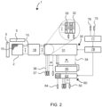
- FIG. 2 shows schematically components of an exemplary image sensor 1 of the invention.
- the image sensor 1 may be a SPAD sensor and may be formed as a system on a chip (SoC). All components described with regard to FIG. 2 may hence be arranged on the same chip.
- the image sensor 1 comprises a SPAD array or sensor array 2 of (photon-counting) detector elements 10 which may be SPADs.
- the sensor array 2 is equipped with masking registers 5.
- Each photon-counting detector element 10 is connected with an output track (output line) 15. When one of the photon-counting detector elements 10 registers an impinging photon, a signal is output via its output track 15.
- the output tracks 15 lead to a monostable unit 18 with a plurality of monostables which serve for shortening signal pulses travelling through the output tracks 15. From the monostables, the output tracks 15 continue to a connection matrix 31 of an electronic module 30.
- the connection matrix 31 allows to flexibly combine the signals from different output tracks 15 and thus from different SPADs.
- the connection matrix 31 includes a matrix of (e.g., logical OR) connections 32 and associated RAM or other memory 33.
- the output tracks 15 of several or all SPADs may be connected to one (OR) connection 32, wherein the memory 33 allows to flexibly set from which of the connected output tracks 15 signals shall be forwarded via the OR connection.
- Each of the OR connections 32 thus outputs via a respective output line 34 a combined signal which is the sum of the signals of the output tracks 15 for which the memory 33 indicates that the respective signals shall be forwarded.
- a signal which is output through one of the output lines 34 the information from which of the combined SPADs a pulse (registered photon) stems, is lost.
- the electronic module 30 also includes a counter 35, which in the depicted example is formed by two banks of counter elements. At least some of the output lines 34 (in the depicted example: eighty output lines 34) of the connection matrix 31 lead to the counter 35.
- the counter 35 counts the number of pulses (registered photons) per output line 34 and outputs a count number. The count number indicates the number of photons registered with the selected number of photon-counting detector elements within a specified time interval. At this point, the information when exactly a photon-counting detector element fired is not preserved.
- timing-aware lines/tracks are drawn with dashed lines, whereas solid lines indicate digital lines in which the exact timing information of a SPAD firing is not preserved. As can be seen, the timing information is lost at the counter 35.
- the digital output of the counter 35 may form an n-bit output word. As described in greater detail later, the n-bit output word is converted to an m-bit code 50 which is output through a read-out system 63 of an output unit 60, also referred to as input/output unit or IO unit.
- a frame 64 may be input to a software component SW.
- connection matrix 31 may be provided with further output lines 36 which do not lead to any counter but instead directly to outputs of the chip; these output lines 36 serve for timing outputs 37. In the depicted example, twenty output lines 36 are provided. The timing information can then be processed by an external module which is not arranged on the chip.
- FIG. 2 further shows that a clock signal 75 and other serial input data 76 may be input through a digital interface 77 to registers 78, and can be further used to set the connection matrix 31 and/or to control the output unit 60.
- the read-out system 63 is configured for single-ended digital communication and comprises several parallel outputs (in the depicted example: 11) for outputting an 11-bit string. Without further measures, outputting information at the read-out system 63 would lead to significant power and ground bouncing as described earlier. To avoid these issues, count values from counter 35 are not directly output. Instead, the count values are mapped onto a code which is output through the read-out system. This code is specially designed to reduce or avoid power and ground bouncing, as will be explained with regard to the following figures.
- FIG. 3 shows schematically components of an exemplary image sensor 1 of the invention which is built as a system on a chip 20.
- FIG. 3 shows an external (electronic) system 80 to which the chip 20 is connected.
- the image sensor 1 and the external system 80 together form an exemplary SPAD sensor device 100 of the invention.
- the image sensor 1 comprises an n-bit to m-bit converter 45 which receives an n-bit word.
- the n-bit word may be an output from the counter 35 / the electronic module 30 shown in FIG. 1 and is thus referred to as an n-bit output word 40.
- the n-bit to m-bit converter 45 converts each n-bit output word 40 into an m-bit code 50.
- the m-bit code 50 is output to the output unit 60.
- the output unit 60 includes a number of at least m output cells 61 with respective pads 62. Each bit of the m-bit code 50 is output through one of the pads 62.
- a parallel single-ended communication through an interface 65 between chip 20 and external system 80 is thus realized.
- the interface 65 may comprise further electrical contacts not shown in the schematic drawing.
- the external system 80 is connected to the pads 62 through pins 66 to receive the m-bit code 50.
- the m-bit code 50 is supplied to an m-bit to n-bit reverse converter 85 which converts the m-bit code 50 back into the n-bit word 40.
- n-bit to m-bit converter 45 generates balanced codes in which the numbers of ones and zeros is well balanced. The transition from one m-bit code to the next will not significantly alter the overall number of high and low outputs at the pads 62.
- the interface 65 thus constitutes a balanced physical interface.
- mapping according to which the n-bit to m-bit converter 45 maps each possible n-bit output word 40 to a unique and balanced m-bit code 50 will be further explained with regard to FIG. 4 .
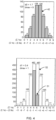
- FIG. 4 shows in its upper portion a histogram 42 for all possible n-bit output words 40 as produced by standard counters.
- the histogram shows how many n-bit output words 40 exist per number of 1s included in the n-bit output words 40.
- the horizontal axis indicates the number of ones within one n-bit output word.
- the number of 1s included in 9-bit output words is between zero (for the 9-bit output word 000000000) and nine (for the 9-bit output word 111111111).
- 1 code/possibility exists for 9-bit output words with zero 1s
- 9 different codes exist for 9-bit output words with one 1
- 36 codes exist for 9-bit output words with two 1s, and so forth.
- n-bit output words 40 were output at pads 62 of output cells, input and output currents would be highly unbalanced and there would be large changes between the number of 1s of consecutive n-bit output words. For example, if a 9-bit output word with three 1s were output followed by a 9-bit output word with seven 1s, the sum of voltages / high outputs at the single-ended communication lines (pads) increased by four, i.e., the voltage is changed to high at four more pads compared with any pads at which the output voltage may be reduced to low or ground, for outputting the next 9-bit output word. This leads to substantial unbalanced currents at the output interface.
- FIG. 4 shows in its lower part a histogram 52 (dashed lines) of all possible m-bit codes, wherein m is 11.
- FIG. 4 also shows a subset 51 (solid lines and crosshatched) within all possible m-bit codes.
- the n-bit to m-bit converter 45 does not use all of the possible m-bit codes forming the histogram 52 but only the m-bit codes included in the subset 51. In other words, only the m-bit codes of the subset 51 can be output by the n-bit to m-bit converter 45.
- the choice of the subset 51 also reduces a change in the difference between 1s and 0s from one 11-bit code to another 11-bit code.
- the depicted subset 51 only uses codes with five 1s (and thus six 0s) or six 1s (and thus five 0s). From one 11-bit code to the next, the total number of 1s in the 11-bit code thus changes at most by +/- 1.
- the pads 62 / the interface 65 there will be in sum only a change of max. one signal that changes between high and low. The power and ground bouncing effect is thus effectively reduced.
- m-bit codes with two different numbers of 1s must be used so that sufficiently many m-bit codes are available to encode all n-bit words.
- the depicted example uses a subset 51 with asymmetric numbers of m-bit codes with five 1s and six 1s.
- the number of m-bit codes with five 1s is more than double as high as the number of m-bit codes with six 1s included in the subset 51. This has the consequence that in more cases there will be no change at all in the number of ones from one transmitted m-bit code to the next transmitted m-bit code, thus minimizing power and ground bouncing.
- FIG. 4 indicates the maximum number dmax of a change in the number of 1s from one code/word to the next.
- dmax is 9 (corresponding to the case that the 9-bit word 000000000 is followed by 111111111).
- dmax is 1 as there can be no larger change than from an 11-bit code with five 1s to an 11-bit code with six 1s, or vice versa.
- FIG. 4 indicates the average difference d0, d1 in the number of 1s from any one word to the next.
- the average difference d0 is 1.7.
- the average difference d1 is shy of 0.4.
- the subset 51 is chosen such that the average difference d1 in the number of 1s between two (randomly drawn) codes of the subset 51 is smaller than the average difference d0 in the number of 1s between two of the n-bit output words.
- the subset may be chosen such that d1 ⁇ 0.5 d0.
- the subset 51 is chosen such that dmax for the subset is at most n/3 as large as dmax for the distribution of all n-bit output words.
- mapping from the n-bit output words 40 to m-bit codes 50 is relevant.
- the specific mapping determines the complexity for converting an n-bit output word 40 to an m-bit code 50. The higher the complexity, the higher the number of electronic components and / or space needed for the n-bit to m-bit converter 45.
- the n-bit to m-bit converter 45 may be formed as an n-bit to m-bit conversion LUT (LUT: look-up table) built purely in hardware, using a number of logical components to process any input n-bit word to output a specific m-bit code.
- LUT look-up table
- a favorable mapping between n-bit output words and m-bit codes may be generated as follows, wherein xi indicates an n-bit output word and yi indicates an m-bit code:
- process A i.e., for all possible n-bit output words.
- the processes may be performed first for one of the xi, then for the next xi, and so forth.
- process A may be performed for all xi.
- process B is performed for all xi for which no yi was assigned in process A.
- process C is performed for all xi for which no yi was assigned in process A or B. This has the effect that no code yi is assigned through process C which could be better suited for another xi (in process A or B).
- the processes A and/or B determine candidate codes yi which are equally suited to be assigned to a specific xi.
- Several or all of these balanced codes yi may be regarded as candidate codes.
- Candidate codes are determined for several or all codes xi.
- the codes yi to be assigned to the codes yi are selected such that it is avoided (or the occurrence reduced) that all candidate codes for one xi are assigned to other codes xi such that no suitable candidate code remains for the one xi.
- the selection of a code yi out of the candidate codes begins for those xi for which the smallest groups of candidate codes were determined (in process A and/or B). In this way, the probability is higher that one of several candidate codes yi can actually be assigned to every xi.
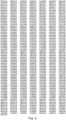
- a table of m-bit codes can be built as shown in FIG. 5 .
- the codes are generated according to processes described with regard to FIG. 4 .
- the 512 codes have a maximum difference of one in their numbers of 1s, i.e., all 512 codes have either five 1s or six 1s.
- This table of converted codes enables the system to balance the number of transitions from 0 to 1 and from 1 to 0 when transmitting a sequence of words. Ideally, if the total input and output currents are fully compensated, the number of transitions are fully evened out and the sum of currents is equal to 0.
- FIG. 6 shows in its upper part a histogram H n-b it of the transitions for a 9-bit regular counter or a Linear Shift Feedback Register (LSFR) counter.
- the horizontal axis indicates the difference d which is the number of 0-1 transitions minus the number of 1-0 transitions between two consecutive codes (here: between two consecutive 9-bit output words).
- the lower part of FIG. 6 shows a histogram H m-b it_ subse t of the transitions for the 11-bit codes of the subset used to encode all 9-bit output words.
- the horizontal axis again indicates the difference d which is the number of zero-to-one transitions minus the number of one-to-zero transitions between two consecutive codes (here: between two consecutive 11-bit codes of the subset).
- the vertical axis indicates the frequency of occurrence (normalized to 1).
- the difference d is zero in 64% of all possible transitions, and d is -1 or +1 in the remaining 36% of all cases. This means that the current at the output interface of the chip is perfectly balanced for 64% of the time and it is not balanced by only 1 unit of current (positive or negative) for 36% of the time.
- the asymmetry between input and output currents can be measured with the standard deviation STD of the distributions H n-b it and H m-bit _ subset .
- the standard deviation STD is 3.5.
- the standard deviation STD for H m-bit _ subset is 0.61 in this exemplary implementation of the invention. This quantifies the extreme improvement in minimizing undesired effects such as power and ground bouncing associated with current changes at the output interface of the chip.
- the LUT (n-bit to m-bit converter 45) comprises an input 46 at which an n-bit output word 40 is input.
- the LUT translates the n-bit output word 40 into an m-bit code 50 which is output at an output 49 of the LUT.
- the LUT comprises a plurality of electrical lines 47 and logical units 48 such as AND or OR units which process the received n-bit output word 40 to form the m-bit code 50.
- a mapping between n-bit output words 40 and m-bit codes 50 is fixed and defined through the configuration of the electrical lines 47 and logical units 48.
- the LUT is purely realized through electronic hardware components, i.e., a mapping and transformation from an n-bit output word 40 to an m-bit code 50 is defined by the hardware, and the LUT does not include any software processes to transform n-bit output words 40 to m-bit codes 50.
- the previously described procedure in generating the mapping between n-bit output words 40 to m-bit codes 50, wherein a bit sequence of an n-bit output word is preferably included in the m-bit codes of the balanced subset, is important for minimizing the complexity of the LUT.
- the final area of the circuit of the LUT / n-bit to m-bit converter 45 is merely 60 x 60 ⁇ m 2 when built in 180nm technology. Furthermore, any time delay due to the code transformation is particularly low.
- FIG. 8 shows schematically components of an exemplary image sensor which may be formed as described with regard to any of the preceding figures.
- FIG. 8 depicts some photon-counting detector elements 10 which are directly connected to pads 62 for outputting signals from these photon-counting detector elements 10.
- the direct connections are in particular used for timing information about firing photon-counting detector elements 10. Direct connections are understood such that signals from the depicted photon-counting detector elements 10 are not led to a counter or other electronic components which translate the signal into a more complex digital code or otherwise process the signal such that timing information would not be preserved.
- the photon-counting detector elements 10 are grouped into a first group G1 and a second group G2.
- the photon-counting detector elements 10 of the first group G1 are configured to be active-high H, meaning their output signal is only high upon registration of a photon.
- the photon-counting detector elements 10 of the second group G2 are configured to be active-low L such that their outputs are high as long as no photon is registered and becomes low when a photon is detected.
- outputs of the photon-counting detector elements 10 of the second group G2 may be inverted, e.g., with inverters I as depicted.
- the photon-counting detector elements 10 of the first group G1 do not comprise inverters but instead buffers B.
- both groups G1 and G2 comprise the same number of photon-counting detector elements 10. More generally, the numbers may not deviate from each other by more than 20%. If all of these photon photon-counting detector elements 10 fire at the same time, there will be about the same number of high and low signals output at the pads 20, similar to the case that no photons are registered. Consequently, an intensity change of impinging light does hardly change the overall current at the outputs and thus power and ground bouncing is minimized.
- the compensating effects of the first and second groups G1 and G2 should preferably be achieved irrespective of any light intensity distribution on the sensor array.
- a preferred pattern how the photon-counting detector elements 10 are assigned to the first or second group G1, G2 will be described with regard to the following figure.
- FIG. 9 shows schematically the array 2 of photon-counting detector elements 10 of an exemplary image sensor 1 of the invention.
- Half of all photon-counting detector elements 10 are provided with inverters I so that the polarity at their outputs is inverted and the output signals become active-low.
- photon-counting detector elements 10 with and without inverters alternate.
- the photon-counting detector elements 10 with inverters I may be evenly spread between the photon-counting detector elements 10 without inverters.
- the high and low output signals will be balanced or almost balanced.
- the position of the illumination spot on the array 2 will not affect the desired balance in the output.
- the size of the illumination spot will not or hardly affect the balance.
- Grouping the photon-counting detector elements 10 in two groups may, in one embodiment, only concern those photon-counting detector elements 10 that are not connected to a counter (such as the timing outputs 37 in FIG. 2 ). These photon-counting detector elements 10 may be routed via a connection matrix 31, which is in particular feasible if skew-less lines are provided between the photon-counting detector elements 10 and the connection matrix 31, as described for some embodiments of the invention. To allow for active-low outputs, the connection matrix may in this case not merely include OR connections but further logical units such that a high signal / a count signal is output if any one of the active-high and active-low photon-counting detector elements 10 outputs a signal indicative of the reception of a photon. In other embodiments, the photon-counting detector elements 10 of the two groups are not connected via a connection matrix to the output pads. The array 2 then comprises further photon-counting detector elements 10 which are connected with the connection matrix as described with regard to FIG. 2 .
- FIG. 10 shows a graph with simulated results of the total current balance at the chip output, for the case of an array without any inverters (i.e., all photon-counting detector elements 10 are active-high), and for the array 2 of FIG. 9 (i.e., 50% of active-low photon-counting detector elements 10 distributed evenly between the 50% of active-high photon-counting detector elements 10.
- the horizontal axis in FIG. 10 indicates the number of simultaneously firing photon-counting detector elements 10.
- the vertical axis indicates the units of current i at the output.
- the curve i_con indicates the current at the output interface for a conventional sensor with only active-high SPADs. As shown, the units of current increase proportionally with the activity with no limit. For example, in a system of 362 SPADs, the units of current will increase up to 362 units.
- curve i_inv relates to a case where half of all SPADs are inverted to be active-low.
- the positive and negative currents will tend, with certain probabilities, to compensate one another, thus keeping a mean value of 0 units of current no matter what activity is considered.
- all SPADs are independent and could fire in any random combination, they will not always fully compensate each other.
- the curves +3STD and -3STD indicate the borders within which the current will be in 95% of all theoretically possible cases.
- the theoretically possible cases comprise all possible illumination patterns on the sensor array, while practically possible patterns will enjoy an even better current compensation.
- the +3STD and -3STD boundaries indicate that the inversion of 50% of the outputs of all 362 SPADs as shown in FIG. 9 can reduce the imbalance of units of currents from 181 to 30 or less for 95% of the cases at the worst-case scenario (activity of all SPADs: 50%).
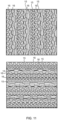
- FIGS. 11 to 13 show schematically output tracks (output lines) 15 of photon-counting detector elements of exemplary embodiments of the image sensor of the invention.
- different lengths (skew) of the output tracks of sensor elements lead to time jitter in the measured signals. This problem may increase when a connection matrix combines the signals from several detector elements; the information from which of several combined detector elements a signal stems is lost, and hence compensation after the connection matrix becomes more difficult or impossible.
- FIGS. 11 to 13 minimizes the global time jitter of the system through length equalization of all output tracks 15 of the photon-counting detector elements.
- the output tracks 15 are provided with wiggles 17 which increase the length of the respective output track 15.
- the output tracks 15 thus are not merely straight lines but include a zig-zag, meandering or otherwise oscillating shape according to the wiggles 17.
- FIG. 11 shows in its upper part output tracks 15 which are vertical tracks of the sensor array, whereas the lower part of FIG. 11 shows output tracks 15 which constitute horizontal tracks of the sensor array.
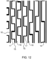
- FIG. 12 A detail of FIG. 11 is shown in FIG. 12 .
- the output tracks 15 would have different lengths if no wiggles 17 were used.
- the wiggles 17 compensate for any skew of the SPAD array.
- the number of wiggles 17 to be added to each output track 15 is calculated by a length equalization algorithm such that each output track 15 has the same length from the respective photon-counting detector element to a connection point (e.g., OR connection) of the connection matrix 31.
- a connection point e.g., OR connection
- the locations of all connections of the connection matrix 31 can be considered: the output track 15 of one photon-counting detector element connects to several (OR) connectors of the connection matrix 31 to allow flexibly binning/combining photon-counting detector elements into macro-pixels.
- the wiggles 17 may be added such that the length of the output track 15 from its photon-counting detector element to each of its (OR) connectors of the connection matrix 31 is the same. Additionally, the wiggles 17 provide for common lengths between the output tracks 15 of different photon-counting detector elements.
- FIGS. 11 to 13 additionally show that ground tracks / lines 16 are added for shielding. Between two neighboring output tracks 15, there is always one ground track 16 which reduces crosstalk between the neighboring output tracks 15.
- the ground tracks 16 include no wiggles as no length equalization is needed.
- the wiggles 17 may be evenly spread along a length of each output track 15, i.e., the bends or turns of the wiggles 17 of one output track 15 may have a common distance from one bend/turn to the next. The more wiggles 17 are added to an output track 15, the shorter the distance between bends/turns of the wiggles 17 of this output track 15.
- the wiggles 17 are formed such that each output track 15 has on average the same distance to both of its neighboring ground tracks 16 for equalizing the fringe capacitance.
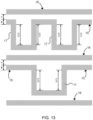
- FIG. 13 shows an enlarged section of two output tracks 15 and neighboring ground tracks 16 for shielding.
- the output track 15 shown in the lower part of FIG. 13 needs to be lengthened by a length S such that its total length matches the length of the longest output track 15. This is achieved by adding one wiggle 17 which comprises two lengthening sections each having a length of S/2.
- the output track 15 shown in the upper part of FIG. 13 is shorter still and needs to be lengthened by 2S for which reason two wiggles 17 are added.
- FIG. 13 also indicates a (minimal) width W of the output tracks 15 and a minimal clearance C between the output track 15 and the neighboring ground track 16.
- the width W may be constant throughout the wiggles 17. While the shown embodiments depict rectangular-shaped wiggles 17, the wiggles 17 may be modified to include rounded edges or to have other forms such as a sinusoidal shape or a saw tooth shape.
- the parasitics to ground are equalized in all of the output tracks 15. Equal proximity to the surrounding ground tracks 16 is ensured along the whole length of the output tracks 15. For this purpose, a minimum number of wiggles 17 may optionally also be added to the longest output track 15 which, in principle, does not need any extra length for the length compensation.
- the compensation achieved for 362 output tracks coming from the SPAD array was 6 ⁇ m of a total length of 800 ⁇ m for the worst-case track.
- the time spread or jitter at Full-Width Half-Maximum (FWHM) was 15 ps in simulations.
- the described length compensation by added wiggles may optionally also be used for other lines of the chip and/or for digital communication, in particular for the output lines of the counters and/or the lines from the connection matrix to the counter unit.
- the detector elements have been described as photon-counting detector elements; however, in general the described examples may be modified such that the detector elements are not photon-counting detector elements.
- an image sensor may comprise the n-bit to m-bit converter described with regard to FIGS. 2 to 7 and/or the SPAD output inversion scheme described with regard to FIGS. 8 to 10 and/or the skew-less output tracks described with regard to FIGS. 11 to 13 .
Landscapes
- Engineering & Computer Science (AREA)
- Multimedia (AREA)
- Signal Processing (AREA)
- Dc Digital Transmission (AREA)
Priority Applications (1)
| Application Number | Priority Date | Filing Date | Title |
|---|---|---|---|
| EP23185791.3A EP4496335B1 (fr) | 2023-07-17 | 2023-07-17 | Capteur d'image et procédé de fabrication d'un capteur d'image |
Applications Claiming Priority (1)
| Application Number | Priority Date | Filing Date | Title |
|---|---|---|---|
| EP23185791.3A EP4496335B1 (fr) | 2023-07-17 | 2023-07-17 | Capteur d'image et procédé de fabrication d'un capteur d'image |
Publications (2)
| Publication Number | Publication Date |
|---|---|
| EP4496335A1 true EP4496335A1 (fr) | 2025-01-22 |
| EP4496335B1 EP4496335B1 (fr) | 2025-12-24 |
Family
ID=87377870
Family Applications (1)
| Application Number | Title | Priority Date | Filing Date |
|---|---|---|---|
| EP23185791.3A Active EP4496335B1 (fr) | 2023-07-17 | 2023-07-17 | Capteur d'image et procédé de fabrication d'un capteur d'image |
Country Status (1)
| Country | Link |
|---|---|
| EP (1) | EP4496335B1 (fr) |
Citations (4)
| Publication number | Priority date | Publication date | Assignee | Title |
|---|---|---|---|---|
| US20050062864A1 (en) * | 2003-09-04 | 2005-03-24 | Keiji Mabuchi | Solid-state image sensing apparatus |
| US20120008007A1 (en) * | 2009-01-30 | 2012-01-12 | Panasonic Corporation | Semiconductor integrated circuit, imaging system, and signal conversion method |
| WO2020151838A1 (fr) | 2019-01-25 | 2020-07-30 | Carl Zeiss Microscopy Gmbh | Microscope optique à éléments détecteurs de comptage de photons et procédé d'imagerie |
| WO2020207571A1 (fr) | 2019-04-09 | 2020-10-15 | Carl Zeiss Microscopy Gmbh | Microscope optique à réseau de capteurs reconfigurable |
-
2023
- 2023-07-17 EP EP23185791.3A patent/EP4496335B1/fr active Active
Patent Citations (4)
| Publication number | Priority date | Publication date | Assignee | Title |
|---|---|---|---|---|
| US20050062864A1 (en) * | 2003-09-04 | 2005-03-24 | Keiji Mabuchi | Solid-state image sensing apparatus |
| US20120008007A1 (en) * | 2009-01-30 | 2012-01-12 | Panasonic Corporation | Semiconductor integrated circuit, imaging system, and signal conversion method |
| WO2020151838A1 (fr) | 2019-01-25 | 2020-07-30 | Carl Zeiss Microscopy Gmbh | Microscope optique à éléments détecteurs de comptage de photons et procédé d'imagerie |
| WO2020207571A1 (fr) | 2019-04-09 | 2020-10-15 | Carl Zeiss Microscopy Gmbh | Microscope optique à réseau de capteurs reconfigurable |
Non-Patent Citations (6)
| Title |
|---|
| "8b/10b encoding", WIKIPEDIA, THE FREE ENCYCLOPEDIA, 2023 |
| A. CARIMATTO ET AL.: "Multipurpose, fully-integrated 128x128 event-driven MD-SiPM with 512 16-bit TDCs with 45 ps LSB and 20 ns gating in 40nm CMOS technology", IEEE SOLID-STATE CIRCUITS LETTERS, vol. 1, no. 12, December 2018 (2018-12-01), XP011724855, DOI: 10.1109/LSSC.2019.2911043 |
| L. H. C. BRAGA ET AL.: "A Fully Digital 8x16 SiPM Array for PET Applications With Per-Pixel TDCs and Real-Time Energy Output", IEEE J. SOLID-STATE CIRCUITS, vol. 49, no. 1, January 2014 (2014-01-01), pages 301 - 314, XP011534946, DOI: 10.1109/JSSC.2013.2284351 |
| M.-J. LEE ET AL.: "High-Performance Back-Illuminated Three-Dimensional Stacked Single-Photon Avalanche Diode Implemented in 45-nm CMOS Technology", IEEE J. SEL. TOP. QUANTUM ELECTRON., vol. 24, no. 6, November 2018 (2018-11-01), pages 1 - 9, XP011683683, DOI: 10.1109/JSTQE.2018.2827669 |
| S. LINDNERC. ZHANGI. M. ANTOLOVICM. WOLFE. CHARBON: "A 252 x 144 SPAD Pixel Flash Lidar with 1728 Dual-Clock 48.8 PS TDCs, Integrated Histogramming and 14.9-to-1 Compression in 180NM CMOS Technology", 2018 IEEE SYMPOSIUM ON VLSI CIRCUITS, June 2018 (2018-06-01), pages 69 - 70, XP033427752, DOI: 10.1109/VLSIC.2018.8502386 |
| UNKNOWN UNKNOWN: "8b/10b encoding", 27 October 2023 (2023-10-27), XP093095787, Retrieved from the Internet <URL:https://en.wikipedia.org/wiki/8b/10b_encoding> * |
Also Published As
| Publication number | Publication date |
|---|---|
| EP4496335B1 (fr) | 2025-12-24 |
Similar Documents
| Publication | Publication Date | Title |
|---|---|---|
| KR101648066B1 (ko) | 아날로그-디지털 컨버터 및 이를 포함하는 이미지 센서 | |
| US9153539B2 (en) | Ground-referenced single-ended signaling connected graphics processing unit multi-chip module | |
| KR102130611B1 (ko) | 아날로그-디지털 변환 회로, 이를 포함하는 이미지 센서 및 이미지 센서의 동작 방법 | |
| US9350958B2 (en) | Solid-state imaging apparatus and camera | |
| Poikela et al. | VeloPix: the pixel ASIC for the LHCb upgrade | |
| US8446506B2 (en) | Solid-state imaging device | |
| Morrison et al. | Multistage linear feedback shift register counters with reduced decoding logic in 130-nm CMOS for large-scale array applications | |
| JP6674224B2 (ja) | 固体撮像装置 | |
| US9467637B2 (en) | Image sensor with multi-shared pixel architecture and dual readout path | |
| KR20120022034A (ko) | 픽셀 데이터의 고속 출력을 위한 이미지 센서 | |
| US10504831B2 (en) | Electronic circuit and camera | |
| US20160232847A1 (en) | Scan Control Line Driving Module and Display Device Including Same | |
| US7250897B2 (en) | CMOS image sensor capable of performing analog correlated double sampling | |
| CN103166642B (zh) | 一种红外焦平面读出电路的模数转换电路 | |
| KR20190086136A (ko) | 이미지 센서의 픽셀 어레이 및 이를 포함하는 이미지 센서 | |
| CN103528691B (zh) | 红外焦平面阵列读出电路的行选通信号产生电路 | |
| US20040217895A1 (en) | Analog-digital conversion apparatus | |
| EP4496335B1 (fr) | Capteur d'image et procédé de fabrication d'un capteur d'image | |
| US8330834B2 (en) | Signal processing method and solid-state image sensing device | |
| EP1975780B1 (fr) | Générateur de nombres aléatoires | |
| US20190281246A1 (en) | Image sensing device | |
| US20230023133A1 (en) | Signal processing device and sensing module | |
| KR101377269B1 (ko) | 고속으로 대용량의 직렬 데이터를 전송할 수 있는 이미지센서 | |
| US6594807B1 (en) | Method for minimizing clock skew for an integrated circuit | |
| Ikebe et al. | Image sensor/digital logic 3D stacked module featuring inductive coupling channels for high speed/low-noise image transfer |
Legal Events
| Date | Code | Title | Description |
|---|---|---|---|
| PUAI | Public reference made under article 153(3) epc to a published international application that has entered the european phase |
Free format text: ORIGINAL CODE: 0009012 |
|
| STAA | Information on the status of an ep patent application or granted ep patent |
Free format text: STATUS: THE APPLICATION HAS BEEN PUBLISHED |
|
| AK | Designated contracting states |
Kind code of ref document: A1 Designated state(s): AL AT BE BG CH CY CZ DE DK EE ES FI FR GB GR HR HU IE IS IT LI LT LU LV MC ME MK MT NL NO PL PT RO RS SE SI SK SM TR |
|
| STAA | Information on the status of an ep patent application or granted ep patent |
Free format text: STATUS: REQUEST FOR EXAMINATION WAS MADE |
|
| 17P | Request for examination filed |
Effective date: 20250409 |
|
| GRAP | Despatch of communication of intention to grant a patent |
Free format text: ORIGINAL CODE: EPIDOSNIGR1 |
|
| STAA | Information on the status of an ep patent application or granted ep patent |
Free format text: STATUS: GRANT OF PATENT IS INTENDED |
|
| RIC1 | Information provided on ipc code assigned before grant |
Ipc: H04N 25/00 20230101AFI20250724BHEP Ipc: H04N 25/773 20230101ALI20250724BHEP Ipc: H04N 25/78 20230101ALI20250724BHEP Ipc: H04N 25/76 20230101ALI20250724BHEP |
|
| INTG | Intention to grant announced |
Effective date: 20250827 |
|
| GRAS | Grant fee paid |
Free format text: ORIGINAL CODE: EPIDOSNIGR3 |
|
| GRAA | (expected) grant |
Free format text: ORIGINAL CODE: 0009210 |
|
| STAA | Information on the status of an ep patent application or granted ep patent |
Free format text: STATUS: THE PATENT HAS BEEN GRANTED |
|
| AK | Designated contracting states |
Kind code of ref document: B1 Designated state(s): AL AT BE BG CH CY CZ DE DK EE ES FI FR GB GR HR HU IE IS IT LI LT LU LV MC ME MK MT NL NO PL PT RO RS SE SI SK SM TR |
|
| REG | Reference to a national code |
Ref country code: CH Ref legal event code: F10 Free format text: ST27 STATUS EVENT CODE: U-0-0-F10-F00 (AS PROVIDED BY THE NATIONAL OFFICE) Effective date: 20251224 Ref country code: GB Ref legal event code: FG4D |
|
| REG | Reference to a national code |
Ref country code: DE Ref legal event code: R096 Ref document number: 602023010020 Country of ref document: DE |
|
| REG | Reference to a national code |
Ref country code: LT Ref legal event code: MG9D |
|
| PG25 | Lapsed in a contracting state [announced via postgrant information from national office to epo] |
Ref country code: NO Free format text: LAPSE BECAUSE OF FAILURE TO SUBMIT A TRANSLATION OF THE DESCRIPTION OR TO PAY THE FEE WITHIN THE PRESCRIBED TIME-LIMIT Effective date: 20260324 |
|
| PG25 | Lapsed in a contracting state [announced via postgrant information from national office to epo] |
Ref country code: HR Free format text: LAPSE BECAUSE OF FAILURE TO SUBMIT A TRANSLATION OF THE DESCRIPTION OR TO PAY THE FEE WITHIN THE PRESCRIBED TIME-LIMIT Effective date: 20251224 Ref country code: FI Free format text: LAPSE BECAUSE OF FAILURE TO SUBMIT A TRANSLATION OF THE DESCRIPTION OR TO PAY THE FEE WITHIN THE PRESCRIBED TIME-LIMIT Effective date: 20251224 |
|
| PG25 | Lapsed in a contracting state [announced via postgrant information from national office to epo] |
Ref country code: RS Free format text: LAPSE BECAUSE OF FAILURE TO SUBMIT A TRANSLATION OF THE DESCRIPTION OR TO PAY THE FEE WITHIN THE PRESCRIBED TIME-LIMIT Effective date: 20260324 |
|
| PG25 | Lapsed in a contracting state [announced via postgrant information from national office to epo] |
Ref country code: LV Free format text: LAPSE BECAUSE OF FAILURE TO SUBMIT A TRANSLATION OF THE DESCRIPTION OR TO PAY THE FEE WITHIN THE PRESCRIBED TIME-LIMIT Effective date: 20251224 |