EP4501504A1 - Outil de coupe - Google Patents
Outil de coupe Download PDFInfo
- Publication number
- EP4501504A1 EP4501504A1 EP23934299.1A EP23934299A EP4501504A1 EP 4501504 A1 EP4501504 A1 EP 4501504A1 EP 23934299 A EP23934299 A EP 23934299A EP 4501504 A1 EP4501504 A1 EP 4501504A1
- Authority
- EP
- European Patent Office
- Prior art keywords
- layer
- unit
- less
- thickness
- unit layer
- Prior art date
- Legal status (The legal status is an assumption and is not a legal conclusion. Google has not performed a legal analysis and makes no representation as to the accuracy of the status listed.)
- Pending
Links
- 238000005520 cutting process Methods 0.000 title claims abstract description 256
- 239000011248 coating agent Substances 0.000 claims abstract description 143
- 238000000576 coating method Methods 0.000 claims abstract description 143
- 239000013078 crystal Substances 0.000 claims abstract description 47
- 229910014587 C1-aNa Inorganic materials 0.000 claims abstract description 25
- 239000000203 mixture Substances 0.000 claims description 147
- ZOXJGFHDIHLPTG-UHFFFAOYSA-N Boron Chemical group [B] ZOXJGFHDIHLPTG-UHFFFAOYSA-N 0.000 claims description 14
- 229910052796 boron Inorganic materials 0.000 claims description 14
- 229910052684 Cerium Inorganic materials 0.000 claims description 10
- 229910052727 yttrium Inorganic materials 0.000 claims description 10
- GWXLDORMOJMVQZ-UHFFFAOYSA-N cerium Chemical group [Ce] GWXLDORMOJMVQZ-UHFFFAOYSA-N 0.000 claims description 9
- 229910052746 lanthanum Chemical group 0.000 claims description 9
- FZLIPJUXYLNCLC-UHFFFAOYSA-N lanthanum atom Chemical group [La] FZLIPJUXYLNCLC-UHFFFAOYSA-N 0.000 claims description 9
- VWQVUPCCIRVNHF-UHFFFAOYSA-N yttrium atom Chemical group [Y] VWQVUPCCIRVNHF-UHFFFAOYSA-N 0.000 claims description 9
- 229910052757 nitrogen Inorganic materials 0.000 abstract description 13
- 238000000034 method Methods 0.000 description 41
- 238000012545 processing Methods 0.000 description 33
- 230000000694 effects Effects 0.000 description 27
- 238000005259 measurement Methods 0.000 description 22
- 239000007789 gas Substances 0.000 description 21
- 230000035882 stress Effects 0.000 description 21
- 239000010936 titanium Substances 0.000 description 20
- 125000004429 atom Chemical group 0.000 description 19
- XKRFYHLGVUSROY-UHFFFAOYSA-N Argon Chemical compound [Ar] XKRFYHLGVUSROY-UHFFFAOYSA-N 0.000 description 16
- IJGRMHOSHXDMSA-UHFFFAOYSA-N Atomic nitrogen Chemical compound N#N IJGRMHOSHXDMSA-UHFFFAOYSA-N 0.000 description 16
- 230000003647 oxidation Effects 0.000 description 16
- 238000007254 oxidation reaction Methods 0.000 description 16
- 238000012360 testing method Methods 0.000 description 16
- 239000000463 material Substances 0.000 description 14
- 229910052799 carbon Inorganic materials 0.000 description 13
- 239000012535 impurity Substances 0.000 description 12
- 238000004519 manufacturing process Methods 0.000 description 12
- 238000011161 development Methods 0.000 description 10
- 230000018109 developmental process Effects 0.000 description 10
- 230000001105 regulatory effect Effects 0.000 description 10
- OKTJSMMVPCPJKN-UHFFFAOYSA-N Carbon Chemical compound [C] OKTJSMMVPCPJKN-UHFFFAOYSA-N 0.000 description 9
- 238000005336 cracking Methods 0.000 description 9
- 229910052786 argon Inorganic materials 0.000 description 8
- VNWKTOKETHGBQD-UHFFFAOYSA-N methane Chemical compound C VNWKTOKETHGBQD-UHFFFAOYSA-N 0.000 description 8
- 238000003801 milling Methods 0.000 description 8
- 238000005240 physical vapour deposition Methods 0.000 description 8
- 238000007733 ion plating Methods 0.000 description 7
- 238000000691 measurement method Methods 0.000 description 7
- 150000004767 nitrides Chemical class 0.000 description 7
- 230000002401 inhibitory effect Effects 0.000 description 6
- 229910052710 silicon Inorganic materials 0.000 description 6
- 229910052719 titanium Inorganic materials 0.000 description 6
- 230000005540 biological transmission Effects 0.000 description 5
- 230000001771 impaired effect Effects 0.000 description 5
- ATJFFYVFTNAWJD-UHFFFAOYSA-N Tin Chemical compound [Sn] ATJFFYVFTNAWJD-UHFFFAOYSA-N 0.000 description 4
- 239000011195 cermet Substances 0.000 description 4
- 238000006243 chemical reaction Methods 0.000 description 4
- 230000000052 comparative effect Effects 0.000 description 4
- 239000002826 coolant Substances 0.000 description 4
- 238000000921 elemental analysis Methods 0.000 description 4
- 238000005516 engineering process Methods 0.000 description 4
- 230000008020 evaporation Effects 0.000 description 4
- 238000001704 evaporation Methods 0.000 description 4
- 238000001755 magnetron sputter deposition Methods 0.000 description 4
- 229910021645 metal ion Inorganic materials 0.000 description 4
- 239000012495 reaction gas Substances 0.000 description 4
- 238000005001 rutherford backscattering spectroscopy Methods 0.000 description 4
- QVGXLLKOCUKJST-UHFFFAOYSA-N atomic oxygen Chemical compound [O] QVGXLLKOCUKJST-UHFFFAOYSA-N 0.000 description 3
- 150000001875 compounds Chemical class 0.000 description 3
- 238000007599 discharging Methods 0.000 description 3
- 238000000168 high power impulse magnetron sputter deposition Methods 0.000 description 3
- 229910052751 metal Inorganic materials 0.000 description 3
- 239000002184 metal Substances 0.000 description 3
- 229910052760 oxygen Inorganic materials 0.000 description 3
- 239000001301 oxygen Substances 0.000 description 3
- 229910004205 SiNX Inorganic materials 0.000 description 2
- 229910008482 TiSiN Inorganic materials 0.000 description 2
- 229910009043 WC-Co Inorganic materials 0.000 description 2
- 238000002441 X-ray diffraction Methods 0.000 description 2
- 230000004520 agglutination Effects 0.000 description 2
- 229910045601 alloy Inorganic materials 0.000 description 2
- 239000000956 alloy Substances 0.000 description 2
- 230000015572 biosynthetic process Effects 0.000 description 2
- 125000004432 carbon atom Chemical group C* 0.000 description 2
- 239000003795 chemical substances by application Substances 0.000 description 2
- 238000000151 deposition Methods 0.000 description 2
- 238000013461 design Methods 0.000 description 2
- 230000006866 deterioration Effects 0.000 description 2
- 238000002149 energy-dispersive X-ray emission spectroscopy Methods 0.000 description 2
- 238000011156 evaluation Methods 0.000 description 2
- 238000011835 investigation Methods 0.000 description 2
- QRXWMOHMRWLFEY-UHFFFAOYSA-N isoniazide Chemical compound NNC(=O)C1=CC=NC=C1 QRXWMOHMRWLFEY-UHFFFAOYSA-N 0.000 description 2
- 239000011812 mixed powder Substances 0.000 description 2
- 239000002114 nanocomposite Substances 0.000 description 2
- 239000000843 powder Substances 0.000 description 2
- 238000004663 powder metallurgy Methods 0.000 description 2
- 239000002994 raw material Substances 0.000 description 2
- 238000001228 spectrum Methods 0.000 description 2
- 239000000126 substance Substances 0.000 description 2
- 229910052582 BN Inorganic materials 0.000 description 1
- PZNSFCLAULLKQX-UHFFFAOYSA-N Boron nitride Chemical compound N#B PZNSFCLAULLKQX-UHFFFAOYSA-N 0.000 description 1
- 229910000997 High-speed steel Inorganic materials 0.000 description 1
- 229910052581 Si3N4 Inorganic materials 0.000 description 1
- 229910001069 Ti alloy Inorganic materials 0.000 description 1
- 230000032683 aging Effects 0.000 description 1
- 238000004458 analytical method Methods 0.000 description 1
- 230000003466 anti-cipated effect Effects 0.000 description 1
- 238000005422 blasting Methods 0.000 description 1
- 239000000919 ceramic Substances 0.000 description 1
- 238000005229 chemical vapour deposition Methods 0.000 description 1
- 238000004140 cleaning Methods 0.000 description 1
- 238000010276 construction Methods 0.000 description 1
- PMHQVHHXPFUNSP-UHFFFAOYSA-M copper(1+);methylsulfanylmethane;bromide Chemical compound Br[Cu].CSC PMHQVHHXPFUNSP-UHFFFAOYSA-M 0.000 description 1
- 239000010730 cutting oil Substances 0.000 description 1
- 229910003460 diamond Inorganic materials 0.000 description 1
- 239000010432 diamond Substances 0.000 description 1
- 238000010891 electric arc Methods 0.000 description 1
- 238000010894 electron beam technology Methods 0.000 description 1
- 230000007613 environmental effect Effects 0.000 description 1
- 229910000816 inconels 718 Inorganic materials 0.000 description 1
- 238000010849 ion bombardment Methods 0.000 description 1
- 150000002500 ions Chemical class 0.000 description 1
- 239000000314 lubricant Substances 0.000 description 1
- 230000008018 melting Effects 0.000 description 1
- 238000002844 melting Methods 0.000 description 1
- 238000012986 modification Methods 0.000 description 1
- 230000004048 modification Effects 0.000 description 1
- 229910052758 niobium Inorganic materials 0.000 description 1
- TWNQGVIAIRXVLR-UHFFFAOYSA-N oxo(oxoalumanyloxy)alumane Chemical compound O=[Al]O[Al]=O TWNQGVIAIRXVLR-UHFFFAOYSA-N 0.000 description 1
- 238000005498 polishing Methods 0.000 description 1
- 230000005855 radiation Effects 0.000 description 1
- 239000010703 silicon Substances 0.000 description 1
- HBMJWWWQQXIZIP-UHFFFAOYSA-N silicon carbide Chemical compound [Si+]#[C-] HBMJWWWQQXIZIP-UHFFFAOYSA-N 0.000 description 1
- 229910010271 silicon carbide Inorganic materials 0.000 description 1
- HQVNEWCFYHHQES-UHFFFAOYSA-N silicon nitride Chemical compound N12[Si]34N5[Si]62N3[Si]51N64 HQVNEWCFYHHQES-UHFFFAOYSA-N 0.000 description 1
- 229910052715 tantalum Inorganic materials 0.000 description 1
- MTPVUVINMAGMJL-UHFFFAOYSA-N trimethyl(1,1,2,2,2-pentafluoroethyl)silane Chemical compound C[Si](C)(C)C(F)(F)C(F)(F)F MTPVUVINMAGMJL-UHFFFAOYSA-N 0.000 description 1
- 239000002699 waste material Substances 0.000 description 1
Images


Classifications
-
- B—PERFORMING OPERATIONS; TRANSPORTING
- B23—MACHINE TOOLS; METAL-WORKING NOT OTHERWISE PROVIDED FOR
- B23B—TURNING; BORING
- B23B27/00—Tools for turning or boring machines; Tools of a similar kind in general; Accessories therefor
- B23B27/14—Cutting tools of which the bits or tips or cutting inserts are of special material
- B23B27/148—Composition of the cutting inserts
-
- B—PERFORMING OPERATIONS; TRANSPORTING
- B23—MACHINE TOOLS; METAL-WORKING NOT OTHERWISE PROVIDED FOR
- B23B—TURNING; BORING
- B23B27/00—Tools for turning or boring machines; Tools of a similar kind in general; Accessories therefor
- B23B27/14—Cutting tools of which the bits or tips or cutting inserts are of special material
-
- C—CHEMISTRY; METALLURGY
- C23—COATING METALLIC MATERIAL; COATING MATERIAL WITH METALLIC MATERIAL; CHEMICAL SURFACE TREATMENT; DIFFUSION TREATMENT OF METALLIC MATERIAL; COATING BY VACUUM EVAPORATION, BY SPUTTERING, BY ION IMPLANTATION OR BY CHEMICAL VAPOUR DEPOSITION, IN GENERAL; INHIBITING CORROSION OF METALLIC MATERIAL OR INCRUSTATION IN GENERAL
- C23C—COATING METALLIC MATERIAL; COATING MATERIAL WITH METALLIC MATERIAL; SURFACE TREATMENT OF METALLIC MATERIAL BY DIFFUSION INTO THE SURFACE, BY CHEMICAL CONVERSION OR SUBSTITUTION; COATING BY VACUUM EVAPORATION, BY SPUTTERING, BY ION IMPLANTATION OR BY CHEMICAL VAPOUR DEPOSITION, IN GENERAL
- C23C14/00—Coating by vacuum evaporation, by sputtering or by ion implantation of the coating forming material
- C23C14/06—Coating by vacuum evaporation, by sputtering or by ion implantation of the coating forming material characterised by the coating material
- C23C14/0641—Nitrides
-
- C—CHEMISTRY; METALLURGY
- C23—COATING METALLIC MATERIAL; COATING MATERIAL WITH METALLIC MATERIAL; CHEMICAL SURFACE TREATMENT; DIFFUSION TREATMENT OF METALLIC MATERIAL; COATING BY VACUUM EVAPORATION, BY SPUTTERING, BY ION IMPLANTATION OR BY CHEMICAL VAPOUR DEPOSITION, IN GENERAL; INHIBITING CORROSION OF METALLIC MATERIAL OR INCRUSTATION IN GENERAL
- C23C—COATING METALLIC MATERIAL; COATING MATERIAL WITH METALLIC MATERIAL; SURFACE TREATMENT OF METALLIC MATERIAL BY DIFFUSION INTO THE SURFACE, BY CHEMICAL CONVERSION OR SUBSTITUTION; COATING BY VACUUM EVAPORATION, BY SPUTTERING, BY ION IMPLANTATION OR BY CHEMICAL VAPOUR DEPOSITION, IN GENERAL
- C23C14/00—Coating by vacuum evaporation, by sputtering or by ion implantation of the coating forming material
- C23C14/06—Coating by vacuum evaporation, by sputtering or by ion implantation of the coating forming material characterised by the coating material
- C23C14/0664—Carbonitrides
-
- C—CHEMISTRY; METALLURGY
- C23—COATING METALLIC MATERIAL; COATING MATERIAL WITH METALLIC MATERIAL; CHEMICAL SURFACE TREATMENT; DIFFUSION TREATMENT OF METALLIC MATERIAL; COATING BY VACUUM EVAPORATION, BY SPUTTERING, BY ION IMPLANTATION OR BY CHEMICAL VAPOUR DEPOSITION, IN GENERAL; INHIBITING CORROSION OF METALLIC MATERIAL OR INCRUSTATION IN GENERAL
- C23C—COATING METALLIC MATERIAL; COATING MATERIAL WITH METALLIC MATERIAL; SURFACE TREATMENT OF METALLIC MATERIAL BY DIFFUSION INTO THE SURFACE, BY CHEMICAL CONVERSION OR SUBSTITUTION; COATING BY VACUUM EVAPORATION, BY SPUTTERING, BY ION IMPLANTATION OR BY CHEMICAL VAPOUR DEPOSITION, IN GENERAL
- C23C14/00—Coating by vacuum evaporation, by sputtering or by ion implantation of the coating forming material
- C23C14/22—Coating by vacuum evaporation, by sputtering or by ion implantation of the coating forming material characterised by the process of coating
- C23C14/34—Sputtering
- C23C14/35—Sputtering by application of a magnetic field, e.g. magnetron sputtering
-
- C—CHEMISTRY; METALLURGY
- C23—COATING METALLIC MATERIAL; COATING MATERIAL WITH METALLIC MATERIAL; CHEMICAL SURFACE TREATMENT; DIFFUSION TREATMENT OF METALLIC MATERIAL; COATING BY VACUUM EVAPORATION, BY SPUTTERING, BY ION IMPLANTATION OR BY CHEMICAL VAPOUR DEPOSITION, IN GENERAL; INHIBITING CORROSION OF METALLIC MATERIAL OR INCRUSTATION IN GENERAL
- C23C—COATING METALLIC MATERIAL; COATING MATERIAL WITH METALLIC MATERIAL; SURFACE TREATMENT OF METALLIC MATERIAL BY DIFFUSION INTO THE SURFACE, BY CHEMICAL CONVERSION OR SUBSTITUTION; COATING BY VACUUM EVAPORATION, BY SPUTTERING, BY ION IMPLANTATION OR BY CHEMICAL VAPOUR DEPOSITION, IN GENERAL
- C23C16/00—Chemical coating by decomposition of gaseous compounds, without leaving reaction products of surface material in the coating, i.e. chemical vapour deposition [CVD] processes
- C23C16/22—Chemical coating by decomposition of gaseous compounds, without leaving reaction products of surface material in the coating, i.e. chemical vapour deposition [CVD] processes characterised by the deposition of inorganic material, other than metallic material
- C23C16/30—Deposition of compounds, mixtures or solid solutions, e.g. borides, carbides, nitrides
- C23C16/36—Carbonitrides
-
- C—CHEMISTRY; METALLURGY
- C23—COATING METALLIC MATERIAL; COATING MATERIAL WITH METALLIC MATERIAL; CHEMICAL SURFACE TREATMENT; DIFFUSION TREATMENT OF METALLIC MATERIAL; COATING BY VACUUM EVAPORATION, BY SPUTTERING, BY ION IMPLANTATION OR BY CHEMICAL VAPOUR DEPOSITION, IN GENERAL; INHIBITING CORROSION OF METALLIC MATERIAL OR INCRUSTATION IN GENERAL
- C23C—COATING METALLIC MATERIAL; COATING MATERIAL WITH METALLIC MATERIAL; SURFACE TREATMENT OF METALLIC MATERIAL BY DIFFUSION INTO THE SURFACE, BY CHEMICAL CONVERSION OR SUBSTITUTION; COATING BY VACUUM EVAPORATION, BY SPUTTERING, BY ION IMPLANTATION OR BY CHEMICAL VAPOUR DEPOSITION, IN GENERAL
- C23C28/00—Coating for obtaining at least two superposed coatings either by methods not provided for in a single one of groups C23C2/00 - C23C26/00 or by combinations of methods provided for in subclasses C23C and C25C or C25D
- C23C28/04—Coating for obtaining at least two superposed coatings either by methods not provided for in a single one of groups C23C2/00 - C23C26/00 or by combinations of methods provided for in subclasses C23C and C25C or C25D only coatings of inorganic non-metallic material
- C23C28/042—Coating for obtaining at least two superposed coatings either by methods not provided for in a single one of groups C23C2/00 - C23C26/00 or by combinations of methods provided for in subclasses C23C and C25C or C25D only coatings of inorganic non-metallic material including a refractory ceramic layer, e.g. refractory metal oxides, ZrO2, rare earth oxides
-
- C—CHEMISTRY; METALLURGY
- C23—COATING METALLIC MATERIAL; COATING MATERIAL WITH METALLIC MATERIAL; CHEMICAL SURFACE TREATMENT; DIFFUSION TREATMENT OF METALLIC MATERIAL; COATING BY VACUUM EVAPORATION, BY SPUTTERING, BY ION IMPLANTATION OR BY CHEMICAL VAPOUR DEPOSITION, IN GENERAL; INHIBITING CORROSION OF METALLIC MATERIAL OR INCRUSTATION IN GENERAL
- C23C—COATING METALLIC MATERIAL; COATING MATERIAL WITH METALLIC MATERIAL; SURFACE TREATMENT OF METALLIC MATERIAL BY DIFFUSION INTO THE SURFACE, BY CHEMICAL CONVERSION OR SUBSTITUTION; COATING BY VACUUM EVAPORATION, BY SPUTTERING, BY ION IMPLANTATION OR BY CHEMICAL VAPOUR DEPOSITION, IN GENERAL
- C23C28/00—Coating for obtaining at least two superposed coatings either by methods not provided for in a single one of groups C23C2/00 - C23C26/00 or by combinations of methods provided for in subclasses C23C and C25C or C25D
- C23C28/04—Coating for obtaining at least two superposed coatings either by methods not provided for in a single one of groups C23C2/00 - C23C26/00 or by combinations of methods provided for in subclasses C23C and C25C or C25D only coatings of inorganic non-metallic material
- C23C28/044—Coating for obtaining at least two superposed coatings either by methods not provided for in a single one of groups C23C2/00 - C23C26/00 or by combinations of methods provided for in subclasses C23C and C25C or C25D only coatings of inorganic non-metallic material coatings specially adapted for cutting tools or wear applications
-
- C—CHEMISTRY; METALLURGY
- C23—COATING METALLIC MATERIAL; COATING MATERIAL WITH METALLIC MATERIAL; CHEMICAL SURFACE TREATMENT; DIFFUSION TREATMENT OF METALLIC MATERIAL; COATING BY VACUUM EVAPORATION, BY SPUTTERING, BY ION IMPLANTATION OR BY CHEMICAL VAPOUR DEPOSITION, IN GENERAL; INHIBITING CORROSION OF METALLIC MATERIAL OR INCRUSTATION IN GENERAL
- C23C—COATING METALLIC MATERIAL; COATING MATERIAL WITH METALLIC MATERIAL; SURFACE TREATMENT OF METALLIC MATERIAL BY DIFFUSION INTO THE SURFACE, BY CHEMICAL CONVERSION OR SUBSTITUTION; COATING BY VACUUM EVAPORATION, BY SPUTTERING, BY ION IMPLANTATION OR BY CHEMICAL VAPOUR DEPOSITION, IN GENERAL
- C23C28/00—Coating for obtaining at least two superposed coatings either by methods not provided for in a single one of groups C23C2/00 - C23C26/00 or by combinations of methods provided for in subclasses C23C and C25C or C25D
- C23C28/40—Coatings including alternating layers following a pattern, a periodic or defined repetition
- C23C28/42—Coatings including alternating layers following a pattern, a periodic or defined repetition characterized by the composition of the alternating layers
-
- C—CHEMISTRY; METALLURGY
- C23—COATING METALLIC MATERIAL; COATING MATERIAL WITH METALLIC MATERIAL; CHEMICAL SURFACE TREATMENT; DIFFUSION TREATMENT OF METALLIC MATERIAL; COATING BY VACUUM EVAPORATION, BY SPUTTERING, BY ION IMPLANTATION OR BY CHEMICAL VAPOUR DEPOSITION, IN GENERAL; INHIBITING CORROSION OF METALLIC MATERIAL OR INCRUSTATION IN GENERAL
- C23C—COATING METALLIC MATERIAL; COATING MATERIAL WITH METALLIC MATERIAL; SURFACE TREATMENT OF METALLIC MATERIAL BY DIFFUSION INTO THE SURFACE, BY CHEMICAL CONVERSION OR SUBSTITUTION; COATING BY VACUUM EVAPORATION, BY SPUTTERING, BY ION IMPLANTATION OR BY CHEMICAL VAPOUR DEPOSITION, IN GENERAL
- C23C30/00—Coating with metallic material characterised only by the composition of the metallic material, i.e. not characterised by the coating process
- C23C30/005—Coating with metallic material characterised only by the composition of the metallic material, i.e. not characterised by the coating process on hard metal substrates
Definitions
- the present disclosure relates to a cutting tool.
- a cutting tool comprising a base and a coating disposed on the base has been conventionally used for cutting processing (PTL 1).
- a cutting tool according to an aspect of the present disclosure is a cutting tool comprising:
- Cutting processing serves a central role among manufacturing technology, and evolution of the technology and further sophistication have been continuously required.
- high speed, high efficiency, high precision processing, and ultrafine processing have been basically required.
- workpiece becomes difficult to cut, and countermeasures therefor are also required.
- Sustainable Development Goals SDGs
- the sustainable development means construction of the social basement that does not impair resources needed for the future generation and that is durable against threads of nature.
- improvement of the cutting processing technology expected is reduction in environmental load such as saving power during product manufacturing derived from reduction in steps, and reduction in waste from cutting processing.
- development of a coating material for a tool that has a high high-temperature hardness and that has both of hardness and toughness has been directed in order to lengthen a lifetime of the tool.
- a nitride film mainly composed of Ti and Si is proposed (PTL 1).
- a temperature on a cutting edge of the cutting tool during cutting tends to be high because: dry processing without cutting oil agent is required from the viewpoint of SDGs and global environment conservation; a cutting rate becomes higher for improvement of cutting efficiency; and workpiece becomes diverse, specifically, cutting a so-called hard-to-cut material such as heat-resistant alloy and titanium alloy increases in the aircraft field and the medical field.
- the temperature on the cutting edge becomes high, the lifetime of the cutting tool becomes considerably short. Therefore, a cutting tool that can exhibit excellent tool lifetime even under such severe cutting conditions is required.
- the cutting tool that has a long tool lifetime even in cutting processing performed particularly under conditions of a high temperature on the cutting edge can be provided.
- the cutting tool that has a long tool lifetime even in cutting processing performed particularly under conditions of a high temperature on the cutting edge can be provided.
- the cutting tool can have a longer tool lifetime.
- the cutting tool can have a longer tool lifetime.
- the cutting tool can have a longer tool lifetime.
- the cutting tool can have a longer tool lifetime.
- the cutting tool can have a longer tool lifetime.
- a cutting tool according to another aspect of the present disclosure is a cutting tool comprising:
- the cutting tool that has a long tool lifetime even in cutting processing performed particularly under conditions of a high temperature on the cutting edge can be provided.
- a ratio ⁇ 3/ ⁇ 1 of a thickness ⁇ 3 ⁇ m of the third unit layer to a thickness ⁇ 1 ⁇ m of the first unit layer may be 1.0 or more and 5.0 or less.
- the cutting tool can have a longer tool lifetime.
- M may represent silicon.
- the cutting tool can have a longer tool lifetime.
- M may represent boron
- the cutting tool can have a longer tool lifetime.
- the cutting tool can have a longer tool lifetime.
- the cutting tool can have a longer tool lifetime.
- the cutting tool can have a longer tool lifetime.
- the cutting tool can have a longer tool lifetime.
- the cutting tool can have a longer tool lifetime.
- a description in the form of "A to B" herein means an upper and lower limits of a range (that is, A or more and B or less).
- a has no description of a unit and only B has a description of a unit the unit of A and the unit of B are same.
- any conventionally known atomic ratios are included unless the atomic ratio is particularly limited, and should not be necessarily limited to an atomic ratio within a stoichiometric range.
- a cutting tool 1 according to an embodiment of the present disclosure (hereinafter, also referred to as "Embodiment 1") is a cutting tool comprising:
- Cutting tool 1 of Embodiment 1 can have a long tool lifetime even in cutting processing performed particularly under conditions of a high temperature on the cutting edge. The reason is presumed as follows.
- First unit layer 12 is composed of W(C 1-a N a ) x . Since first unit layer 12 contains C (carbon), a frictional coefficient on a contacting interface with workpiece can be reduced to reduce cutting resistance. In addition, since W(C 1-a N a ) x contains N (nitrogen), the heat resistance is improved by approximately 150°C compared with WC. As a result, the first layer that includes the first unit layer can improve agglutination resistance, a sliding property, and wear resistance in process in which the cutting edge becomes hot, such as dry cutting processing. Thus, the cutting tool that includes the first layer has an improved tool lifetime.
- Second unit layer 15 is composed of Ti c Si 1-c N ("c" represents 0.80 or more and 0.99 or less). Second unit layer 15 has a so-called nanocomposite structure in which nanometer-sized cubic TiN crystals and amorphous SiN x are mixed. Since having extremely increased hardness, second unit layer 15 has an excellent balance between wear resistance, heat shielding property, oxidation resistance, and toughness. Thus, the cutting tool that includes second unit layer 15 has an improved tool lifetime.
- First layer 13 is composed of the alternate layer in which first unit layer 12 and second unit layer 15 are alternately stacked. On an interface between first unit layer 12 and second unit layer 15, the compositions and the crystal lattices are discontinuous. Thus, when cracking occurs from a surface of coating 3 during cutting, the interface can inhibit development of the cracking. The coating that includes the first layer inhibits chipping and breakage. Thus, the cutting tool that includes first layer 13 has an improved tool lifetime.
- Coating 3 can cover at least a part involved in cutting in base 2.
- Coating 3 may cover an entire surface of base 2.
- the constitution of coating 3 that partially differs does not depart from the scope of the present embodiment.
- the part involved in cutting in base 2 herein means a region where a distance from a cutting edge ridgeline is at least within 50 ⁇ m, within 100 ⁇ m, or within 300 ⁇ m on a surface of base 2.
- Cutting tool 1 of the present embodiment can be suitably used as cutting tool 1 such as a drill, an endmill, an indexable cutting insert for a drill, an indexable cutting insert for an endmill, an indexable cutting insert for milling, an indexable cutting insert for turning, a metal saw, a gear-cutting tool, a reamer, and a tap.
- base 2 may be composed of any of cemented carbide (such as WC-based cemented carbide, cemented carbide that contains WC and Co, cemented carbide in which a carbonitride of Ti, Ta, Nb, or the like is added into WC and Co), cermet (that contains TiC, TiN, TiCN, or the like as a main component), high-speed steel, ceramics (such as titanium carbide, silicon carbide, silicon nitride, aluminum nitride, and aluminum oxide), a cubic boron nitride sintered material, or a diamond sintered material.
- cemented carbide such as WC-based cemented carbide, cemented carbide that contains WC and Co, cemented carbide in which a carbonitride of Ti, Ta, Nb, or the like is added into WC and Co
- cermet that contains TiC, TiN, TiCN, or the like as a main component
- high-speed steel ceramics (such as titanium carbide, silicon carbide, silicon nit
- Base 2 may be particularly a WC-based cemented carbide or cermet (particularly, TiCN-based cermet). Since having particularly excellent balance between hardness and strength at high temperature, the WC-based cemented carbide or the cermet can contribute to lengthening of the lifetime of cutting tool 1 when used as base 2 of cutting tool 1.
- Coating 3 of Embodiment 1 includes first layer 13. Coating 3 has an effect of improving properties of cutting tool 1 such as wear resistance and chipping resistance to lengthen the lifetime of cutting tool 1 by covering base 2.
- Coating 3 may include another layer in addition to first layer 13.
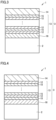
- the other layer include: a second layer 16 disposed between base 2 and first layer 13; and a third layer 14 provided on a side opposite to base 2 of first layer 13, as illustrated in Fig. 3 and Fig. 4 .
- Coating 3 may have an entire thickness of 0.4 ⁇ m or more and 15 ⁇ m or less.
- the entire thickness of coating 3 is 0.4 ⁇ m or more, the effect of lengthening the lifetime of cutting tool 1 by providing coating 3 is easily obtained. Meanwhile, when the entire thickness of coating 3 is 15 ⁇ m or less, chipping on coating 3 in initial cutting hardly occurs, and the lifetime of cutting tool 1 can be lengthened.
- the entire thickness of coating 3 can be measured by observing a cross section of coating 3 by using a scanning electron microscope (SEM).
- SEM scanning electron microscope
- a specific measurement method is as follows. Cutting tool 1 is cut in a direction along a normal line of the surface of coating 3 to prepare a cross-sectional sample. The cross-sectional sample is observed with an SEM. The observation magnification is 5,000 to 10,000, and the measurement field is 100 to 500 ⁇ m 2 . Thickness widths of coating 3 are measured at three positions in one field, and an average value of the thickness widths at the three positions is calculated. The average value corresponds to the thickness of coating 3. A thickness of each layer described later is measured in the same manner unless otherwise specified.
- a compressive residual stress of coating 3 may be 6 GPa or less in an absolute value.
- the compressive residual stress of coating 3 is a kind of internal stress (specific strain) present in an entirety of coating 3, and refers to a stress represented by a "-" (negative) value (unit: "GPa” is used in the present embodiment).
- a concept of a large compressive residual stress represents a large absolute value of the value
- a concept of a small compressive residual stress represents a small absolute value of the value. That is, the absolute vale of the compressive residual stress of 6 GPa or less means that the compressive residual stress of coating 3 is -6 GPa or more and 0 GPa or less.
- the compressive residual stress of coating 3 is measured by a sin 2 ⁇ method using an X-ray residual stress apparatus (see “ X-Ray Stress Measurement” (The Society of Materials Science, Japan, published in 1981 by Yokendo Ltd. Publishers) pp. 54 to 66 ).
- First unit layer 12 may have a hexagonal crystal structure. When first unit layer 12 has a hexagonal crystal structure, wear resistance of coating 3 is improved. Second unit layer 15 may contain a cubic crystal structure. When second unit layer 15 has a cubic crystal structure, hardness of coating 3 is improved. The crystal structure of each layer in coating 3 can be analyzed with an X-ray diffraction apparatus known in the field.
- the hardness of coating 3 yields a large effect at 30 GPa or more and 55 GPa or less, and the hardness may be 35 GPa or more and 50 GPa or less. According to this, coating 3 has sufficient hardness.
- the hardness of an entirety of coating 3 is measured by a nano-indenter method (Nano Indenter XP, manufactured by MTS Systems Corporation). Specifically, the measurement is performed by a method in accordance with ISO14577, the measurement load is 10 mN (1 gf), hardness on the surface of coating 3 is measured at three positions, and an average value of the hardness at the three positions is calculated. The average value corresponds to the hardness of coating 3.
- First layer 13 of the present embodiment is composed of the alternate layer in which first unit layer 12 and second unit layer 15 are alternately stacked.
- First layer 13 composed of the alternate layer in which first unit layer 12 and second unit layer 15 are alternately stacked can be confirmed by difference in contrast by observing a flake sample that contains a cross section of coating 3 with a transmission electron microscope (TEM).
- TEM transmission electron microscope
- first unit layer 12 and second unit layer 15 may be disposed at a position closest to the side of base 2.
- first unit layer 12 is disposed directly on base 2.
- second unit layer 15 is disposed directly on base 2.
- Any of first unit layer 12 and second unit layer 15 may be disposed on the surface side of coating 3.
- second unit layer 15 is disposed on the surface side of coating 3.
- first unit layer 12 is disposed on the surface side of coating 3.
- a thickness of first layer 13 may be 0.5 ⁇ m or more and 15 ⁇ m or less. When the thickness of first layer 13 is 0.5 ⁇ m or more, excellent wear resistance can be exhibited in continuous processing. When the thickness of first layer 13 is 15 ⁇ m or less, the cutting tool can have excellent chipping resistance in intermittent cutting.
- the thickness of first layer 13 is measured by observing the cross section of coating 3 using a transmission electron microscope (TEM).
- TEM transmission electron microscope
- a specific measurement method is as follows. Cutting tool 1 is cut in a direction along a normal line of the surface of coating 3 to prepare a flake sample that contains the cross section of coating 3. The flake sample is observed with a TEM. The observation magnification is 20,000 to 5,000,000, and the measurement field is 0.0016 to 80 ⁇ m 2 . Thickness widths of first layer 13 are measured at three positions in one field, and an average value of the thickness widths at the three positions is calculated. The average value corresponds to the thickness of first layer 13.
- first unit layer 12 can also be identified to have the hexagonal crystal structure.
- Examples of the apparatus used for the X-ray diffraction measurement include "SmartLab” (trade name), manufactured by Rigaku Corporation.
- the conditions of the XRD measurement are as follows.
- Scanning axis 2 ⁇ - ⁇ X-ray source : Cu-K ⁇ radiation (1.541862 ⁇ )
- Detector 0-dimensional detector (scintillation counter)
- Tube voltage 45 kV
- Tube current 40 mA
- Incident optics utilizing mirror
- Receiving light optics utilizing analyzer crystal (PW3098/27)
- Step 0.03° Scanning time : 2 seconds
- Scanning range (2 ⁇ ) 10° to 120°
- First unit layer 12 is composed of W(C 1-a N a ) x , wherein "a” represents 0.3 or more and 0.8 or less, and “x” represents 0.8 or more and 1.2 or less. According to this, the crystal structure of first unit layer 12 becomes hexagonal, and heat resistance, oxidation resistance, and wear resistance of first unit layer 12 can be improved.
- a lower limit of "a” is 0.3 or more, may be 0.35 or more, may be 0.40 or more, or may be 0.45 or more.
- An upper limit of "a” is 0.8 or less, may be 0.75 or less, may be 0.70 or less, or may be 0.65 or less.
- “a” may be 0.35 or more and 0.75 or less, may be 0.40 or more and 0.70 or less, or may be 0.45 or more and 0.65 or less.
- a lower limit of "x” is 0.8 or more, may be 0.85 or more, or may be 0.90 or more.
- An upper limit of "x” is 1.2 or less, may be 1.15 or less, or may be 1.10 or less.
- “x” may be 0.85 or more and 1.15 or less, may be 0.90 or more and 1.10 or less, or may be 1.00.
- first unit layer 12 is composed of W(C 1-a N a ) x
- first unit layer 12 may contain an inevitable impurity in addition to W(C 1-a N a ) x as long as the effect of the present disclosure is not impaired.
- the inevitable impurity include oxygen and carbon.
- a content rate of an entirety of the inevitable impurity in first unit layer 12 may be larger than 0 atom% and less than 1 atom%.
- atom% herein means a proportion (%) of the number of atoms relative to a total number of atoms to constitute the layer.
- Second unit layer 15 is composed of Ti c Si 1-c N, and "c" represents 0.80 or more and 0.99 or less. Second unit layer 15 can improve heat shielding property, oxidation resistance, and toughness of coating 3.
- a lower limit of "c” is 0.80 or more, may be 0.81 or more, may be 0.82 or more, may be 0.85 or more, or may be 0.88 or more.
- An upper limit of "c” is 0.99 or less, may be 0.95 or less, may be 0.93 or less, or may be 0.90 or less.
- “c” may be 0.81 or more, may be 0.82 or more and 0.95 or less, may be 0.85 or more and 0.93 or less, or may be 0.88 or more and 0.90 or less.
- the second unit layer is composed of Ti c Si 1-c N
- second unit layer 15 may contain an inevitable impurity in addition to Ti c Si 1-c N as long as the effect of the present disclosure is not impaired.
- the inevitable impurity include oxygen and carbon.
- a content rate of an entirety of the inevitable impurity in second unit layer 15 may be larger than 0 atom% and less than 1 atom%.
- the "a”, the “x”, the “c”, the content rate of the inevitable impurity in first unit layer 12, and the content rate of the inevitable impurity in second unit layer 15 are measured by elemental analysis on the cross section of coating 3 using a transmission electron microscope (TEM).
- TEM transmission electron microscope
- a specific measurement method is as follows. Cutting tool 1 is cut in a direction along a normal line of the surface of coating 3 to prepare a flake sample that contains the cross section of coating 3. The flake sample is irradiated with electron beam by using energy dispersive X-ray spectroscopy (EDS) attached to the TEM, and energy and generation time of characteristic X-ray generated in this time are measured to perform elemental analysis on first unit layer 12 and second unit layer 15.
- EDS energy dispersive X-ray spectroscopy
- first unit layers 12 and five second unit layers 15 are randomly selected to perform the elemental analysis.
- An average composition of the five first unit layers 12 is determined. This average composition corresponds to the composition of first unit layer 12.
- An average composition of the five second unit layers 15 is determined. This average composition corresponds to the composition of second unit layer 15.
- the elemental analysis is performed on all the layers to determine average compositions of first unit layers 12 and second unit layers 15. As long as an identical cutting tool 1 is measured, it has been confirmed that the measurement results have no variation even by randomly selecting the measurement positions.
- a ratio A N1 /A M1 of a total number A N1 of atoms of C and N relative to a number A M1 of atoms of W is 0.8 or more and 1.2 or less.
- a ratio A N2 /A M2 of a number A N2 of atoms of N relative to a total number A M2 of atoms of Ti and Si is necessarily 0.8 or more and 1.2 or less in manufacturing.
- the ratio A N1 /A M1 and the ratio A N2 /A M2 can be measured by a Rutherford backscattering (RBS) method.
- RBS Rutherford backscattering
- An average thickness of first unit layers 12 may be 0.002 ⁇ m or more and 0.2 ⁇ m or less, and an average thickness of second unit layers 15 may be 0.002 ⁇ m or more and 0.2 ⁇ m or less. According to this, development of cracking generated on the surface of coating 3 can be further inhibited.
- a lower limit of the average thickness of first unit layers 12 may be 0.002 ⁇ m or more, may be 0.005 ⁇ m or more, or may be 0.01 ⁇ m or more.
- An upper limit of the average thickness of first unit layers 12 may be 0.20 ⁇ m or less, may be 0.15 ⁇ m or less, or may be 0.10 ⁇ m or less.
- the average thickness of first unit layers 12 may be 0.005 ⁇ m or more and 0.15 ⁇ m or less, or may be 0.01 ⁇ m or more and 0.1 ⁇ m or less.
- a lower limit of the average thickness of second unit layers 15 may be 0.002 ⁇ m or more, may be 0.005 ⁇ m or more, or may be 0.01 ⁇ m or more.
- An upper limit of the average thickness of second unit layers 15 may be 0.20 ⁇ m or less, may be 0.15 ⁇ m or less, or may be 0.10 ⁇ m or less.
- the average thickness of second unit layers 15 may be 0.005 ⁇ m or more and 0.15 ⁇ m or less, or may be 0.01 ⁇ m or more and 0.10 ⁇ m or less.
- the average thickness of first unit layers 12 and the average thickness of second unit layers 15 can be measured by the method same as the measurement method of the thickness of first layer 13.
- a ratio ⁇ 2/ ⁇ 1 of a thickness ⁇ 2 ⁇ m of second unit layer 15 to a thickness ⁇ 1 ⁇ m of first unit layer 12 may be 1.0 or more and 5.0 or less.
- Second unit layer 15 has high oxidation resistance, and in addition, low thermal conductivity and has a property of hardly conducting heat generated during cutting toward base 2.
- the ratio ⁇ 2/ ⁇ 1 is 1.0 or more, a proportion of second unit layer 15 in coating 3 relatively increases, resulting in improvement of a heat shielding property as an entirety of cutting tool 1.
- Cutting tool 1 that has coating 3 has particularly improved wear resistance in continuous cutting.
- ⁇ 2/ ⁇ 1 may be 1.0 or more, may be 1.1 or more, may be 1.2 or more, may be 1.3 or more, may be 1.4 or more, may be 1.5 or more, may be 2.0 or more, or may be 2.5 or more.
- ⁇ 2/ ⁇ 1 may be 5.0 or less, may be 4.0 or less, or may be 3.0 or less.
- ⁇ 2/ ⁇ 1 may be 1.2 or more and 4.0 or less, or may be 1.5 or more and 2.5 or less.
- the thicknesses ⁇ 1 of three first unit layers 12 are not needed to be equal, and the thicknesses ⁇ 2 of three second unit layers 15 are not needed to be equal as long as the above relationship of ⁇ 2/ ⁇ 1 is satisfied between the first unit layer and the second unit layer adjacent to each other.
- the number of stacking of each of first unit layers 12 and second unit layers 15 may be 5 or more and 500 or less, or may be 10 or more and 500 or less. According to this, stacking of first unit layers 12 and second unit layers 15 can sufficiently yield an effect of improving the hardness and the compressive residual stress with good balance. In first layer 13, the number of stacking of each of first unit layers 12 and second unit layers 15 may be 100 or more and 400 or less, or may be 200 or more and 350 or less.
- first layer 13 the number of stacking of each of first unit layers 12 and second unit layers 15 can be determined by observing the flake sample of the cross section of coating 3 using a transmission electron microscope (TEM) with an observation magnification of 20,000 to 5,000,000.
- TEM transmission electron microscope
- coating 3 may further include a second layer 16 disposed between base 2 and first layer 13, and a composition of second layer 16 may be same as a composition of first unit layer 12 or a composition of second unit layer 15. According to this, adhesiveness between base 2 and coating 3 can be improved.
- second layer 16 When the composition of second layer 16 is same as the composition of first unit layer 12, second layer 16 has a good sliding property even when second layer 16 is exposed in initial cutting, and thereby wear resistance can be improved.
- a thickness of second layer 16 may be larger than the thickness of first unit layer 12. According to this, adhesiveness between base 2 and coating 3 can be further increased. Since second layer 16 has a good sliding property even when second layer 16 is exposed in initial cutting, wear resistance can be improved.
- the term "the thickness of the second layer is larger than the thickness of the first unit layer” can be rephrased to "the thickness of the second layer is more than 1.0 time larger than the thickness of the first unit layer”.
- the thickness of second layer 16 may be 2.0 times or more, may be 4.0 times or more, or may be 10.0 times or more larger than the thickness of first unit layer 12.
- the thickness of second layer 16 may be 500 times or less, may be 120 times or less, or may be 50 times or less larger than the thickness of first unit layer 12.
- the thickness of second layer 16 may be 2.0 times or more and 500 times or less, may be 4.0 times or more and 120 times or less, or may be 10.0 times or more and 50 times or less larger than the thickness of first unit layer 12.
- the thickness of second layer 16 may be 0.1 ⁇ m or more. If the thickness of second layer 16 is less than 0.1 ⁇ m, the effect of improving wear resistance by setting second layer 16 to have the same composition as first unit layer 12 tends to be difficult to obtain.
- the thickness of second layer 16 may be 0.3 ⁇ m or more, or may be 0.4 ⁇ m or more.
- An upper limit value of the thickness of second layer 16 is not particularly limited, but more than 2 ⁇ m enlarges the crystal grains to generate a grain boundary, which tends to be difficult to obtain the effect of improving wear resistance. Thus, with considering a cost aspect, the thickness of second layer 16 may be 2 ⁇ m or less.
- first unit layer 12 may be stacked directly on second layer 16, as illustrated in Fig. 3 .
- second unit layer 15 may also be stacked directly on second layer 16.
- second layer 16 and first unit layer 12 have a continuous crystal structure.
- the thickness of second layer 16 may be larger than the thickness of second unit layer 15. According to this, adhesiveness between base 2 and coating 3 can be further increased. In addition, even when second layer 16 is exposed in initial cutting, oxidation from the interface between base 2 and coating 3 can be inhibited and the cutting heat can be shielded.
- the term "the thickness of the second layer is larger than the thickness of the second unit layer” can be rephrased to "the thickness of the second layer is more than 1.0 time larger than the thickness of the second unit layer”.
- the thickness of second layer 16 may be 2.0 times or more, may be 4.0 times or more, or may be 10.0 times or more larger than the thickness of second unit layer 15.
- the thickness of second layer 16 may be 500 times or less, may be 120 times or less, or may be 50 times or less larger than the thickness of second unit layer 15.
- the thickness of second layer 16 may be 2.0 times or more and 500 times or less, may be 4.0 times or more and 120 times or less, or may be 10.0 times or more and 50 times or less larger than the thickness of second unit layer 15.
- the thickness of second layer 16 may be 0.1 ⁇ m or more. If the thickness of second layer 16 is less than 0.1 ⁇ m, the effect of inhibiting the oxidation from the interface between base 2 and coating 3 and the effect of shielding the cutting heat by setting second layer 16 to have the same composition as second unit layer 15 tend to be difficult to obtain.
- the thickness of second layer 16 may be 0.3 ⁇ m or more, or may be 0.4 ⁇ m or more.
- An upper limit value of the thickness of second layer 16 is not particularly limited, but more than 2 ⁇ m enlarges the crystal grains to generate a grain boundary, which tends to be difficult to further improve the effect of inhibiting the oxidation.
- the thickness of second layer 16 may be 2 ⁇ m or less.
- first unit layer 12 may be stacked directly on second layer 16, as illustrated in Fig. 3 .
- second unit layer 15 may also be stacked directly on second layer 16.
- second layer 16 and second unit layer 15 have a continuous crystal structure.
- coating 3 may further include a third layer 14 provided on a side opposite to base 2 of first layer 13, and third layer 14 may be composed of TiSiCN. According to this, a frictional coefficient of coating 3 can be reduced to attempt to lengthen the lifetime of cutting tool 1.
- a carbonitride typically tends to have a lower frictional coefficient against workpiece than a nitride. Such lowering of the frictional coefficient is presumably derived from contribution of the carbon atoms.
- Coating 3 that includes third layer 14 lowers the frictional coefficient of coating 3 against the workpiece to lengthen the lifetime of cutting tool 1.
- third layer 14 regulating a composition ratio between N and C enables to impart a predetermined color. According to this, design properties and distinctive properties can be imparted to appearance of cutting tool 1, which yields commercial usefulness.
- a thickness of third layer 14 may be 0.1 ⁇ m or more.
- an effect of imparting lubricity by third layer 14 is easily obtained.
- an upper limit value of the thickness of third layer 14 is not particularly limited, but more than 2 ⁇ m tends to fail to further improve the aforementioned effect of imparting lubricity.
- the thickness of third layer 14 may be 2 ⁇ m or less with considering a cost aspect.
- Coating 3 may include an intermediate layer disposed between second layer 16 and first layer 13, or between first layer 13 and third layer 14.
- the intermediate layer include TiSiCeN, TiSiN, TiSiBN, TiSiYN, and TiSiLaN.
- a thickness of the intermediate layer may be 0.1 ⁇ m or more and 2 ⁇ m or less, may be 0.3 ⁇ m or more and 1.5 ⁇ m or less, or may be 0.4 ⁇ m or more and 1.0 ⁇ m or less.
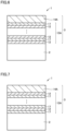
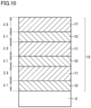
- a cutting tool according to another embodiment of the present disclosure will be described by using Fig. 6 to Fig. 10 .
- a cutting tool 1 according to another embodiment (hereinafter, also referred to as "Embodiment 2") of the present disclosure is cutting tool 1 comprising:
- Cutting tool 1 of Embodiment 1 can have a long tool lifetime even in cutting processing performed particularly under conditions of a high temperature on the cutting edge. The reason is presumed as follows.
- First unit layer 12 is composed of W(C 1-a N a ) x . Since first unit layer 12 contains C (carbon), a frictional coefficient on a contacting interface with workpiece can be reduced to reduce cutting resistance. In addition, since W(C 1-a N a ) x contains N (nitrogen), the heat resistance is improved by approximately 150°C compared with WC. As a result, the first layer that includes the first unit layer can improve wear resistance in process in which the cutting edge becomes hot, such as dry cutting processing. Thus, the cutting tool that includes the first layer has an improved tool lifetime.
- TiSiN layer a layer composed of a nitride of Ti and Si
- TiSiMN layer a layer composed of a nitride that contains Ti, Si, and M (M represents boron, yttrium, cerium, or lanthanum)
- TiSiMN layer a layer composed of a nitride that contains Ti, Si, and M (M represents boron, yttrium, cerium, or lanthanum)
- first A layer 13A can have the characteristics of first unit layer 12, which are high hardness and low friction, and the characteristics of third unit layer 17, which are a high heat shielding property.
- the characteristics of the small compressive residual stress of third unit layer 17 can be compensated by the large compressive residual stress of first unit layer 12. Therefore, the hardness, the heat shielding property, and the compressive residual stress are improved with good balance as an entirety of first A layer 13A, and the lifetime of cutting tool 1 that includes first A layer 13A is further lengthened.
- Third unit layer 17 has a so-called nanocomposite structure in which nanometer-sized cubic TiN crystals and amorphous SiNx are mixed. Since having extremely increased hardness, third unit layer 17 has an excellent balance between wear resistance, heat shielding resistance, oxidation resistance, and toughness. Thus, the cutting tool that includes third unit layer 17 can achieve a long tool lifetime.
- First A layer 13A is composed of the alternate layer in which first unit layer 12 and third unit layer 17 are alternately stacked.
- the compositions and the crystal lattices are discontinuous.
- the interface can inhibit development of the cracking. Therefore, chipping and breakage are inhibited to further lengthen the lifetime of cutting tool 1.
- Cutting tool 1 of Embodiment 2 may have basically same constitution as cutting tool 1 of Embodiment 1 except for constitution of first A layer 13A, second A layer 16, and third A layer 14A.
- first A layer “first A layer”, “second A layer”, and “third A layer” will be described.
- First A layer 13A of the present embodiment is composed of the alternate layer in which first unit layer 12 and third unit layer 17 are alternately stacked.
- First A layer 13A composed of the alternate layer in which first unit layer 12 and third unit layer 17 are alternately stacked can be confirmed by difference in contrast by observing a cross section of coating 3 with a transmission electron microscope (TEM).
- a thickness of first A layer 13A may have same constitution as the thickness of first layer 13 described in Embodiment 1.
- composition W(C 1-a N a ) x of first unit layer 12 of Embodiment 2 may be same as the composition W(C 1-a N a ) x of first unit layer 12 of Embodiment 1.
- Third unit layer 17 is composed of Ti d Si 1-d-e M e N, wherein M represents boron, yttrium, cerium, or lanthanum, "d” represents 0.80 or more and 0.99 or less, and "e” represents more than 0 and 0.05 or less. Third unit layer 17 can have both of excellent hardness and excellent oxidation resistance. The reason is presumed as follows.
- boron increases hardness of third unit layer 17 to increase hardness of an entirety of coating 3.
- An oxide of boron formed by oxidation on the surface of cutting tool 1 in cutting densifies an oxide of Al in third unit layer 17 to improve oxidation resistance of third unit layer 17. Furthermore, since having a low melting point, the oxide of boron serves as a lubricant during cutting, and can inhibit agglutination of workpiece.
- a lattice constant of YN is 4.88 ⁇
- a lattice constant of CeN is 5.01 ⁇
- a lattice constant of LaN is 5.30 ⁇ .
- the lattice constants of YN, CeN, and LaN are larger than a lattice constant of TiN, 4.23 ⁇ .
- the “d” is 0.80 or more and 0.99 or less. According to this, the crystal structure of third unit layer 17 becomes cubic to increase hardness of third unit layer 17 and improve wear resistance.
- a lower limit of “d” is 0.80 or more, may be 0.82 or more, may be 0.85 or more, or may be 0.87 or more.
- An upper limit of “d” is 0.99 or less, may be 0.95 or less, may be 0.92 or less, or may be 0.90 or less.
- “d” may be 0.82 or more and 0.95 or less, may be 0.85 or more and 0.92 or less, or may be 0.87 or more and 0.90 or less.
- the "e” is more than 0 and 0.05 or less. According to this, hardness and oxidation resistance of first A layer 13A can be improved.
- a lower limit of “e” may be 0.002 or more, may be 0.005 or more, may be 0.01 or more, or may be 0.02 or more.
- the “e” may be 0.04 or less, or may be 0.03 or less.
- “e” may be 0.002 or more and 0.05 or less, may be 0.01 or more and 0.05 or less, may be 0.01 or more and 0.03 or less, or may be 0.02 or more and 0.03 or less.
- the third unit layer is composed of Ti d Si 1-d-e M e N
- third unit layer 17 may contain an inevitable impurity in addition to Ti d Si 1-d-e M e N as long as the effect of the present disclosure is not impaired.
- the inevitable impurity include oxygen and carbon.
- a content rate of an entirety of the inevitable impurity in third unit layer 17 may be larger than 0 atom% and less than 1 atom%.
- the content rates of the "d", the “e”, and the inevitable impurity in third unit layer 17 are determined in the same method as the measurement method of the "a". As long as an identical cutting tool 1 is measured, it has been confirmed that the measurement results have no variation even by randomly selecting the measurement positions.
- a ratio A N1 /A M1 of a total number A N1 of atoms of C and N relative to a number A M1 of atoms of W is 0.8 or more and 1.2 or less.
- a ratio A N3 /A M3 of a number A N3 of atoms of N relative to a total number A M3 of atoms of Ti, Si, and M is necessarily 0.8 or more and 1.2 or less in manufacturing.
- the ratio A N1 /A M1 and the ratio A N3 /A M3 can be measured by a Rutherford backscattering (RBS) method.
- RBS Rutherford backscattering
- An average thickness of first unit layers 12 may be 0.002 ⁇ m or more and 0.2 ⁇ m or less, and an average thickness of third unit layers 17 may be 0.002 ⁇ m or more and 0.2 ⁇ m or less. According to this, development of cracking generated on the surface of coating 3 can be further inhibited.
- a lower limit of the average thickness of first unit layers 12 may be 0.002 ⁇ m or more, may be 0.005 ⁇ m or more, or may be 0.01 ⁇ m or more.
- An upper limit of the average thickness of first unit layers 12 may be 0.20 ⁇ m or less, may be 0.15 ⁇ m or less, or may be 0.10 ⁇ m or less.
- the average thickness of first unit layers 12 may be 0.005 ⁇ m or more and 0.15 ⁇ m or less, or may be 0.01 ⁇ m or more and 0.1 ⁇ m or less.
- a lower limit of the average thickness of third unit layers 17 may be 0.002 ⁇ m or more, may be 0.005 ⁇ m or more, or may be 0.01 ⁇ m or more.
- An upper limit of the average thickness of third unit layers 17 may be 0.20 ⁇ m or less, may be 0.15 ⁇ m or less, or may be 0.10 ⁇ m or less.
- the average thickness of third unit layers 17 may be 0.005 ⁇ m or more and 0.15 ⁇ m or less, or may be 0.01 ⁇ m or more and 0.10 ⁇ m or less.
- the average thickness of first unit layers 12 and the average thickness of third unit layers 17 can be determined by a method same as the measurement method of the thickness of first layer 13.
- a ratio ⁇ 3/ ⁇ 1 of a thickness ⁇ 3 of third unit layer 17 to a thickness ⁇ 1 of first unit layer 12 may be 1.0 or more and 5.0 or less.
- Third unit layer 17 has high oxidation resistance, and in addition, low thermal conductivity and has a property of hardly conducting heat generated during cutting toward base 2.
- the ratio ⁇ 3/ ⁇ 1 is 1.0 or more, a proportion of third unit layer 17 in coating 3 relatively increases to increase an Al amount in coating 3, resulting in improvement of a heat shielding property as an entirety of cutting tool 1.
- Cutting tool 1 that has coating 3 has particularly improved wear resistance in continuous cutting.
- ⁇ 3/ ⁇ 1 may be 1.0 or more, may be 1.1 or more, may be 1.2 or more, may be 1.3 or more, may be 1.4 or more, may be 1.5 or more, or may be 2.0 or more.
- ⁇ 3/ ⁇ 1 may be 5.0 or less, may be 4.0 or less, or may be 3.0 or less.
- ⁇ 3/ ⁇ 1 may be 1.0 or more and 5.0 or less, may be 1.2 or more and 4.0 or less, may be 1.5 or more and 4.0 or less, may be 1.0 or more and 3.0 or less, or may be 2.0 or more and 3.0 or less.
- the thicknesses ⁇ 1 of three first unit layers 12 are not needed to be equal, and the thicknesses ⁇ 3 of three third unit layers 17 are not needed to be equal as long as the above relationship of ⁇ 3/ ⁇ 1 is satisfied between the first unit layer and the third unit layer adjacent to each other.
- the number of stacking of each of first unit layers 12 and third unit layers 17 may be 4 or more and 800 or less, or may be 10 or more and 500 or less. According to this, stacking of first unit layers 12 and third unit layers 17 tends to easily yield an effect of improving the hardness and the compressive residual stress with good balance. In first A layer 13A, the number of stacking of each of first unit layers 12 and third unit layers 17 may be 100 or more and 400 or less, or may be 200 or more and 350 or less.
- first A layer 13A the number of stacking of each of first unit layers 12 and third unit layers 17 can be determined in the same method as the method of measuring the number of stacking of each of first unit layers 12 and second unit layers 15 described in Embodiment 1.
- coating 3 may further include a second A layer 16A disposed between base 2 and first A layer 13A, and a composition of second A layer 16A may be same as a composition of first unit layer 12 or a composition of third unit layer 17. According to this, adhesiveness between base 2 and coating 3 can be improved.
- second A layer 16A When the composition of second A layer 16A is same as the composition of first unit layer 12, second A layer 16A has a good sliding property even when second A layer 16A is exposed in initial cutting, and thereby wear resistance can be improved.
- a thickness of second A layer 16A may be larger than the thickness of first unit layer 12. According to this, adhesiveness between base 2 and coating 3 can be further improved. Since second A layer 16A has a good sliding property even when second A layer 16A is exposed in initial cutting, wear resistance can be improved.
- the term "the thickness of the second A layer is larger than the thickness of the first unit layer” can be rephrased to "the thickness of the second A layer is more than 1.0 time larger than the thickness of the first unit layer”.
- the thickness of second A layer 16A may be 2.0 times or more, may be 4.0 times or more, or may be 10.0 times or more larger than the thickness of first unit layer 12.
- the thickness of second A layer 16A may be 500 times or less, may be 120 times or less, or may be 50 times or less larger than the thickness of first unit layer 12.
- the thickness of second A layer 16A may be 2.0 times or more and 500 times or less, may be 4.0 times or more and 120 times or less, or may be 10.0 times or more and 50 times or less larger than the thickness of first unit layer 12.
- the thickness of second A layer 16A may be 0.1 ⁇ m or more. If the thickness of second A layer 16A is less than 0.1 ⁇ m, the effect of improving wear resistance by setting second A layer 16A to have the same composition as first unit layer 12 tends to be difficult to obtain.
- the thickness of second A layer 16A may be 0.3 ⁇ m or more, or may be 0.4 ⁇ m or more.
- An upper limit value of the thickness of second A layer 16A is not particularly limited, but more than 2 ⁇ m enlarges the crystal grains to generate a grain boundary, which tends to be difficult to obtain the effect of improving wear resistance. Thus, with considering a cost aspect, the thickness of second A layer 16A may be 2 ⁇ m or less.
- first unit layer 12 may be stacked directly on second A layer 16A, as illustrated in Fig. 8 .
- second unit layer 15 may also be stacked directly on second A layer 16A.
- second A layer 16A and first unit layer 12 have a continuous crystal structure.
- composition of second A layer 16A is same as the composition of third unit layer 17
- peeling resistance of coating 3 can be improved particularly in intermittent processing such as milling and endmill processing, which repeatedly applies a load to the cutting edge, because third unit layer 17 tends to have small stress.
- the thickness of second A layer 16A may be larger than the thickness of third unit layer 17. According to this, adhesiveness between base 2 and coating 3 can be further improved. Even when second A layer 16A is exposed in initial cutting, oxidation from an interface between base 2 and coating 3 can be inhibited, and the cutting heat can be shielded.
- the term "the thickness of the second A layer is larger than the thickness of the third unit layer” can be rephrased to "the thickness of the second A layer is more than 1.0 time larger than the thickness of the third unit layer".
- the thickness of second A layer 16A may be 2.0 times or more, may be 4.0 times or more, or may be 10.0 times or more larger than the thickness of third unit layer 17.
- the thickness of second A layer 16A may be 500 times or less, may be 120 times or less, or may be 50 times or less larger than the thickness of third unit layer 17.
- the thickness of second A layer 16A may be 2.0 times or more and 500 times or less, may be 4.0 times or more and 120 times or less, or may be 10.0 times or more and 50 times or less larger than the thickness of third unit layer 17.
- the thickness of second A layer 16A may be 0.1 ⁇ m or more. If the thickness of second A layer 16A is less than 0.1 ⁇ m, the effect of inhibiting the oxidation from the interface between base 2 and coating 3 and the effect of shielding the cutting heat by setting second A layer 16A to have the same composition as third unit layer 17 tend to be difficult to obtain.
- the thickness of second A layer 16A may be 0.3 ⁇ m or more, or may be 0.4 ⁇ m or more.
- An upper limit value of the thickness of second A layer 16A is not particularly limited, but more than 2 ⁇ m enlarges the crystal grains to generate a grain boundary, which tends to be difficult to further improve the effect of inhibiting the oxidation.
- the thickness of second A layer 16A may be 2 ⁇ m or less.
- first unit layer 12 may be stacked directly on second A layer 16A, as illustrated in Fig. 8 .
- third unit layer 17 may also be stacked directly on second A layer 16A.
- second A layer 16A and third unit layer 17 have a continuous crystal structure.
- coating 3 may further include a third A layer 14A provided on a side opposite to base 2 of first layer 13, and third A layer 14A may be composed of TiSiMeCN.
- Me may represent boron, yttrium, cerium, or lanthanum.
- Me may be the same element as M used in the third unit layer. According to this, a frictional coefficient of coating 3 can be reduced to attempt to lengthen the lifetime of cutting tool 1.
- a carbonitride typically tends to have a lower frictional coefficient against workpiece than a nitride. Such lowering of the frictional coefficient is presumably derived from contribution of the carbon atoms.
- Coating 3 that includes third A layer 14A lowers the frictional coefficient of coating 3 against the workpiece to lengthen the lifetime of cutting tool 1.
- a thickness of third A layer 14A may be 0.1 ⁇ m or more.
- an effect of imparting lubricity by third A layer 14A is easily obtained.
- an upper limit value of the thickness of third A layer 14A is not particularly limited, but more than 2 ⁇ m tends to fail to further improve the aforementioned effect of imparting lubricity.
- the thickness of third A layer 14A may be 2 ⁇ m or less with considering a cost aspect.
- Embodiment 3 a method for manufacturing cutting tool 1 of Embodiment 1 or Embodiment 2 will be described.
- the manufacturing method comprises: a first step of preparing a base 2; and a second step of forming a coating 3 on base 2.
- the second step comprises a step of forming a first layer 13 or a first A layer 13A.
- base 2 is prepared.
- base 2 described in Embodiment 1 may be used.
- base 2 When a cemented carbide is used as base 2, commercially available bases may be used, or base 2 may be manufactured by a common powder metallurgy method.
- base 2 When base 2 is manufactured by a common powder metallurgy method, WC powder, Co powder, and the like are mixed with a ball mill or the like to obtain a mixed powder. This mixed powder is dried, and then molded into a predetermined shape to obtain a molded article. Thereafter, the molded article is sintered to obtain a WC-Co-based cemented carbide (sintered material). Then, this sintered material may be subjected to a predetermined cutting-edge treatment such as a homing treatment to manufacture a base composed of the WC-Co-based cemented carbide. Any bases conventionally known as such a type of bases, other than the above base, may also be prepared.
- coating 3 is formed on base 2.
- the second step comprises a step of forming first layer 13 or first A layer 13A.
- first unit layer 12 and second unit layer 15 are alternately stacked by using a physical vapor deposition (PVD) method to form first layer 13.
- PVD physical vapor deposition
- first unit layer 12 and third unit layer 17 are alternately stacked by using a PVD method to form first A layer 13A.
- PVD physical vapor deposition
- the present inventors have investigated various methods as a method for forming first layer 13 and first A layer 13A, and consequently found that the layer composed of a compound that has high crystallinity can be formed and coating 3 has excellent wear resistance by using the physical vapor deposition method.
- At least one selected from the group consisting of a cathode arc-ion plating method, a balanced magnetron sputtering method, an unbalanced magnetron sputtering method, and a high power impulse magnetron sputtering (HiPIMS) method may be used.
- a cathode arc-ion plating method that has a high ionization rate of raw material elements may be used.
- an ion bombardment treatment with metal for a surface of base 2 can be performed before first layer 13 or first A layer 13A is formed.
- adhesiveness between base 2 and coating 3 that includes first layer 13 or first A layer 13A is remarkably improved.
- the cathode arc-ion plating method can be performed by: placing base 2 in an apparatus and placing a target as a cathode; and then applying high voltage to the target for generating arc discharge to ionize and evaporate atoms that constitute the target; and depositing a substance on base 2, for example.
- the balanced magnetron sputtering method can be performed by: placing base 2 in an apparatus and placing a target on a magnetron electrode that has a magnet to form a balanced magnetic field; applying high-frequency electric power between the magnetron electrode and base 2 to generate gas plasma; and allowing gas ions generated by generation of this gas plasma to collide with the target; and depositing atoms released from the target on base 2, for example.
- the unbalanced magnetron sputtering method can be performed by setting the magnetic field to be generated by the magnetron electrode to be unbalanced in the aforementioned balanced magnetron spattering method, for example.
- the HiPIMS method which can apply further higher voltage to obtain a dense film, may also be used.
- the second step may comprise, in addition to the step of forming first layer 13 or first A layer 13A, a step of treating a surface of the coating, such as polishing using a brush and a dry or wet shot blasting.
- the second step may also comprise a step of forming other layers such as a second layer 16, a second A layer 16A, a third layer 14, a third A layer 14A, and an intermediate layer.
- the other layers can be formed by conventionally known chemical vapor deposition method or physical vapor deposition method. From the viewpoint of ability of forming the other layer continuously to first unit layer 12, second unit layer 15, or third unit layer 17 in one physical vapor deposition apparatus, the other layer is preferably formed by a physical vapor deposition method.
- Fig. 11 is a schematic cross-sectional view of a cathode arc-ion plating apparatus used in the present Example.
- Fig. 12 is an outline top view of the apparatus in Fig. 11 .
- a cathode 106 for a first unit layer, a cathode 107 for a second unit layer, and a cathode 120 for a third layer, which are alloy targets to be metal raw materials of a coating 3, and a rotary base holder 104 for placing the base are attached in a chamber 101.
- a composition of cathode 106 is adjusted to obtain a composition of the first unit layer in Table 1.
- a composition of cathode 107 is adjusted to obtain a composition of the second unit layer in Table 1.
- a composition of cathode 120 is adjusted to obtain a composition of the third layer in Table 2.
- An arc power source 108 is attached to cathode 106, an arc power source 109 is attached to cathode 107, and an arc power source (not illustrated) is attached to cathode 120.
- a bias power source 110 is attached to base holder 104.
- a gas introducing port 105 to introduce gas 102 is provided and a gas discharging port 103 is provided for regulating a pressure in chamber 101, and chamber 101 has structure in which gas 102 in chamber 101 can be sucked by a vacuum pump through gas discharging port 103.
- base holder 104 On base holder 104, a chip of CNMG120408 that was a cemented carbide of JIS Standard P30 grade and that had JIS Standard shape, and a chip of SEMT13T3AGSN manufactured by Sumitomo Electric Hardmetal Corp. were attached as the base.
- a pressure in chamber 101 was reduced by the vacuum pump, and a temperature was raised to 500°C by a heater placed in the apparatus while rotating the base, and evacuation was performed until the pressure in chamber 101 reached 1.0 ⁇ 10 -4 Pa.
- argon gas was introduced through the gas introducing port to hold the pressure in chamber 101 to be 2.0 Pa, a voltage of bias power source 110 was gradually raised to -1000 V, and cleaning of a surface of the base was performed for 15 minutes. Thereafter, the argon gas was discharged from chamber 101 to clean the base (argon bombard treatment).
- the base of a cutting tool of each sample was prepared.
- a purpose of introducing the argon gas was to clean a surface of a WC cathode used in a case where a first unit layer W(C 1-a N a ) x was formed.
- the base temperature was 400°C, which was lower than a formation temperature of a conventional nitride film, 600°C.
- the reason is as follows.
- the present inventors have found a tendency of deterioration of hardness of a coating when the coating is formed at the base temperature of 600°C.
- the present inventors have investigated the reason, and presumed that, when the coating is formed at the base temperature of 600°C, carbon (C) contained in the cathode for the first unit layer becomes free carbon to precipitate in the formed coating.
- the present inventors have found that a coating that keeps excellent hardness even at high temperature and that has excellent wear resistance can be formed by forming the coating at a base temperature of 400°C.
- the first layer was formed by alternately stacking each of the first unit layers and the second unit layers one by one on the second layer with the number of stacking shown in Table 1.
- the first layer was formed by alternately stacking each of the first unit layers and the second unit layers one by one on the base with the number of stacking shown in Table 1.
- the thickness of the second layer, each thickness and the number of stacking of each of the first unit layers and the second unit layers in the first layer were regulated by a rotation speed of the base. At a time when the thicknesses of the second layer and the first layer reached the thicknesses respectively shown in Table 1 and Table 2, current supplied to the evaporation source was stopped.
- composition of the first unit layer in the cutting tool of each sample was measured by the method described in Embodiment 1 to obtain values of "a” and "x” in W(C 1-a N a ) x .
- the results are shown in the columns “a” and “x” in Table 1.
- Table 1 a case where "-" are described in the column “a” and the column “x” means that the first unit layer is absent.
- composition of the second unit layer in the cutting tool of each sample was measured by the method described in Embodiment 1 to obtain a value of "c” in Ti c Si 1-c N.
- the results are shown in the column “c” in Table 1.
- Table 1 a case where "-" is described in the column “c” means that the second unit layer is absent.
- compositions of the second layer and the third layer in the cutting tool of each sample were determined by the method described in Embodiment 1. The results are shown in the column “Composition” of "Second layer” and the column “Composition” of "Third layer” in Table 2. A case where "-" is described in the column “Composition” of "Second layer” in Table 2 means that the second layer is absent, and a case where "-" is described in the column “Composition” of "Third layer” means that the third layer is absent.
- the number of stacking of each of the first unit layers and second unit layers in the cutting tool of each sample was determined by the method described in Embodiment 1.
- the number of stacking of 10 represents that the alternate layer includes 10 first unit layers and 10 second unit layers.
- the obtained results are each shown in the column "Number of stacking" in Table 1.
- the average thickness of the first unit layers, the average thickness of the second unit layers, the thickness of the first layer, the thickness of the second layer, and the thickness of the third layer were determined by the method described in Embodiment 1.
- the obtained results are shown in the columns “Average thickness [ ⁇ m]” of "First unit layer”, “Average thickness [ ⁇ m]” of “Second unit layer”, and “Thickness [ ⁇ m]” of "First layer” in Table 1, and “Thickness [ ⁇ m]” of "Second layer”, and “Thickness [ ⁇ m]” of "Third layer” in Table 2.
- ⁇ 2/ ⁇ 1 of the cutting tool of each sample was determined by the method described in Embodiment 1. The obtained results are shown in the column “ ⁇ 2/ ⁇ 1" in Table 1.
- Table 1 a case where "-" is described in the column “ ⁇ 2/ ⁇ 1” means that at least any of the first unit layer and the second unit layer is absent.
- Hardness of the coating of Sample 1 to Sample 25 was measured by the method described in Embodiment 1. The hardness of the coating of these samples was confirmed to be within a range of 30 GPa or more and 55 GPa or less.
- the cutting processing performed under the above cutting conditions is high-speed high-efficiency processing of a hard-to-cut material, and corresponds to cutting processing performed under conditions of high cutting edge temperature.
- the cutting tools of Sample 1 to Sample 25 correspond to Examples, and the cutting tools of Sample 101 to Sample 106 correspond to Comparative Examples.
- the cutting tools of Sample 1 to Sample 25 were confirmed to have a long tool lifetime compared with the cutting tools of Sample 101 to Sample 106 in the cutting processing performed under the conditions of high cutting edge temperature.
- the cutting processing performed under the above cutting conditions is high-speed high-efficiency milling of a hard-to-cut material under a dry condition, and corresponds to cutting processing performed under conditions of high cutting edge temperature.
- the cutting tools of Sample 1 to Sample 25 correspond to Examples, and the cutting tools of Sample 101 to Sample 106 correspond to Comparative Examples.
- the cutting tools of Sample 1 to Sample 25 were confirmed to have a long tool lifetime compared with the cutting tools of Sample 101 to Sample 106 in the cutting processing performed under the conditions of high cutting edge temperature.
- a base of each sample was performed in the same manner as in Example 1.
- arc current was supplied to cathodes 106 and 107 at each 100 A while introducing argon and nitrogen as reaction gases and holding a base temperature at 450°C, a reaction gas pressure at 2.0 Pa, a voltage of bias power source 110 at a predetermined constant value within a range of -50 V to -200 V to generate metal ions from cathodes 106 and 107, and a second A layer and a first A layer that had a composition shown in Table 3 to Table 6 were formed on the base.
- the composition of cathode 106 was regulated so as to obtain the composition of the first unit layer in Table 3 to Table 4.
- the composition of cathode 107 was regulated so as to obtain the composition of the third unit layer in Table 3 to Table 4.
- the composition of cathode 120 was regulated so as to obtain the composition of the third A layer in Table 5 to Table 6.
- the base temperature was 450°C, which was lower than a formation temperature of a conventional nitride film, 600°C. The reason is as follows. The present inventors have found a tendency of deterioration of hardness of a coating when the coating is formed at the base temperature of 600°C.
- the present inventors have investigated the reason, and presumed that, when the coating is formed at the base temperature of 600°C, carbon (C) contained in the cathode for the first unit layer becomes free carbon to precipitate in the formed coating. As a result of intensive investigation, the present inventors have found that a coating that keeps excellent hardness even at high temperature and that has excellent wear resistance can be formed by forming the coating at a base temperature of 450°C.
- the first A layer was formed by alternately stacking each of the first unit layers and the third unit layers one by one on the second A layer with the number of stacking shown in Table 3 to Table 4.
- the first A layer was formed by alternately stacking each of the first unit layers and the third unit layers one by one on the base with the number of stacking shown in Table 3 to Table 4.
- the thickness of the second A layer, each thickness and the number of stacking of the first unit layers and the third unit layers in the first A layer were regulated by a rotation speed of the base. At a time when the thicknesses of the second A layer and the first A layer reached the thicknesses respectively shown in Table 3 to Table 6, current supplied to the evaporation source was stopped.
- Hardness of the coating of Sample 51 to Sample 78 was measured by the method described in Embodiment 1. The hardness of the coating of these samples was confirmed to be within a range of 30 GPa or more and 55 GPa or less.
- the cutting processing performed under the above cutting conditions is high-speed high-efficiency processing of a hard-to-cut material, and corresponds to cutting processing performed under conditions of high cutting edge temperature.
- the cutting tools of Sample 51 to Sample 78 correspond to Examples, and the cutting tools of Sample 151 to Sample 164 correspond to Comparative Examples.
- the cutting tools of Sample 51 to Sample 78 were confirmed to have a long tool lifetime compared with the cutting tools of Sample 151 to Sample 164 in the cutting processing performed under the conditions of high cutting edge temperature.
- the cutting processing performed under the above cutting conditions is high-speed high-efficiency milling of a hard-to-cut material under a dry condition, and corresponds to cutting processing performed under conditions of high cutting edge temperature.
- the cutting tools of Sample 51 to Sample 78 correspond to Examples, and the cutting tools of Sample 151 to Sample 164 correspond to Comparative Examples.
- the cutting tools of Sample 51 to Sample 78 were confirmed to have a long tool lifetime compared with the cutting tools of Sample 151 to Sample 164 in the cutting processing performed under the conditions of high cutting edge temperature.
Landscapes
- Chemical & Material Sciences (AREA)
- Engineering & Computer Science (AREA)
- Mechanical Engineering (AREA)
- Organic Chemistry (AREA)
- Materials Engineering (AREA)
- Metallurgy (AREA)
- Chemical Kinetics & Catalysis (AREA)
- Inorganic Chemistry (AREA)
- Ceramic Engineering (AREA)
- General Chemical & Material Sciences (AREA)
- Cutting Tools, Boring Holders, And Turrets (AREA)
- Physical Vapour Deposition (AREA)
- Drilling Tools (AREA)
Applications Claiming Priority (1)
| Application Number | Priority Date | Filing Date | Title |
|---|---|---|---|
| PCT/JP2023/018432 WO2024236771A1 (fr) | 2023-05-17 | 2023-05-17 | Outil de coupe |
Publications (2)
| Publication Number | Publication Date |
|---|---|
| EP4501504A1 true EP4501504A1 (fr) | 2025-02-05 |
| EP4501504A4 EP4501504A4 (fr) | 2025-02-19 |
Family
ID=92419335
Family Applications (1)
| Application Number | Title | Priority Date | Filing Date |
|---|---|---|---|
| EP23934299.1A Pending EP4501504A4 (fr) | 2023-05-17 | 2023-05-17 | Outil de coupe |
Country Status (5)
| Country | Link |
|---|---|
| US (1) | US12157172B1 (fr) |
| EP (1) | EP4501504A4 (fr) |
| JP (1) | JP7537631B1 (fr) |
| CN (1) | CN119325413A (fr) |
| WO (1) | WO2024236771A1 (fr) |
Families Citing this family (1)
| Publication number | Priority date | Publication date | Assignee | Title |
|---|---|---|---|---|
| JP7807856B1 (ja) * | 2025-09-30 | 2026-01-28 | Seavac株式会社 | 硬質皮膜 |
Family Cites Families (12)
| Publication number | Priority date | Publication date | Assignee | Title |
|---|---|---|---|---|
| JP3950385B2 (ja) | 2002-08-02 | 2007-08-01 | 住友電工ハードメタル株式会社 | 表面被覆切削工具 |
| JP5088481B2 (ja) * | 2007-11-27 | 2012-12-05 | 三菱マテリアル株式会社 | 重切削加工で硬質被覆層がすぐれた耐摩耗性を発揮する表面被覆切削工具 |
| JP5043906B2 (ja) * | 2009-08-27 | 2012-10-10 | 株式会社神戸製鋼所 | 硬質皮膜およびその形成方法 |
| AT510963B1 (de) * | 2011-03-18 | 2012-08-15 | Boehlerit Gmbh & Co Kg | Beschichteter körper und verfahren zu dessen herstellung |
| EP3004412A1 (fr) * | 2013-05-31 | 2016-04-13 | Sandvik Intellectual Property AB | Nouveau procédé de fabrication de carbure cimenté et produit obtenu à partir celui-ci |
| CN105264103A (zh) * | 2013-05-31 | 2016-01-20 | 山特维克知识产权股份有限公司 | 制造硬质合金的新方法及其得到的产品 |
| JP6657594B2 (ja) * | 2014-05-16 | 2020-03-04 | 三菱マテリアル株式会社 | 表面被覆切削工具 |
| JP2017206756A (ja) * | 2016-05-20 | 2017-11-24 | 株式会社神戸製鋼所 | 硬質皮膜及び金型 |
| EP3769877A4 (fr) * | 2018-03-19 | 2021-07-14 | Sumitomo Electric Industries, Ltd. | Outil de coupe revêtu en surface |
| KR20200127840A (ko) * | 2018-03-19 | 2020-11-11 | 스미토모덴키고교가부시키가이샤 | 표면 피복 절삭 공구 |
| JP6813103B2 (ja) * | 2018-03-19 | 2021-01-13 | 住友電気工業株式会社 | 表面被覆切削工具 |
| DE112018007872T5 (de) * | 2018-08-01 | 2021-04-15 | Osg Corporation | Hartbeschichtung und mit Hartbeschichtung bedecktes Element |
-
2023
- 2023-05-17 CN CN202380043284.XA patent/CN119325413A/zh active Pending
- 2023-05-17 JP JP2023560164A patent/JP7537631B1/ja active Active
- 2023-05-17 US US18/568,303 patent/US12157172B1/en active Active
- 2023-05-17 EP EP23934299.1A patent/EP4501504A4/fr active Pending
- 2023-05-17 WO PCT/JP2023/018432 patent/WO2024236771A1/fr not_active Ceased
Also Published As
| Publication number | Publication date |
|---|---|
| US12157172B1 (en) | 2024-12-03 |
| WO2024236771A1 (fr) | 2024-11-21 |
| CN119325413A (zh) | 2025-01-17 |
| US20240383044A1 (en) | 2024-11-21 |
| JP7537631B1 (ja) | 2024-08-21 |
| JPWO2024236771A1 (fr) | 2024-11-21 |
| EP4501504A4 (fr) | 2025-02-19 |
Similar Documents
| Publication | Publication Date | Title |
|---|---|---|
| EP3269479B1 (fr) | Outil de coupe revêtu et procédé de fabrication de celui-ci | |
| EP3763465B1 (fr) | Outil de coupe à revêtement de surface et son procédé de production | |
| EP4494788A1 (fr) | Outil de coupe | |
| EP3763466B1 (fr) | Outil de coupe à revêtement de surface et son procédé de production | |
| EP4501504A1 (fr) | Outil de coupe | |
| EP4501503A1 (fr) | Outil de coupe | |
| EP4434656B1 (fr) | Outil de coupe | |
| EP4585334A1 (fr) | Outil de coupe | |
| EP4582200A1 (fr) | Outil de coupe | |
| EP4588596A1 (fr) | Outil de coupe | |
| EP4703071A1 (fr) | Outil de coupe | |
| EP4400236B1 (fr) | Outil de coupe | |
| EP4450195A1 (fr) | Outil de coupe | |
| EP4434657A1 (fr) | Outil de coupe | |
| US12440901B2 (en) | Cutting tool | |
| EP4506089A1 (fr) | Outil de coupe | |
| EP4527526A1 (fr) | Outil de coupe |
Legal Events
| Date | Code | Title | Description |
|---|---|---|---|
| STAA | Information on the status of an ep patent application or granted ep patent |
Free format text: STATUS: UNKNOWN |
|
| STAA | Information on the status of an ep patent application or granted ep patent |
Free format text: STATUS: THE INTERNATIONAL PUBLICATION HAS BEEN MADE |
|
| PUAI | Public reference made under article 153(3) epc to a published international application that has entered the european phase |
Free format text: ORIGINAL CODE: 0009012 |
|
| STAA | Information on the status of an ep patent application or granted ep patent |
Free format text: STATUS: REQUEST FOR EXAMINATION WAS MADE |
|
| REG | Reference to a national code |
Ref country code: DE Ref legal event code: R079 Free format text: PREVIOUS MAIN CLASS: B23B0027140000 Ipc: C23C0028040000 |
|
| 17P | Request for examination filed |
Effective date: 20241029 |
|
| AK | Designated contracting states |
Kind code of ref document: A1 Designated state(s): AL AT BE BG CH CY CZ DE DK EE ES FI FR GB GR HR HU IE IS IT LI LT LU LV MC ME MK MT NL NO PL PT RO RS SE SI SK SM TR |
|
| A4 | Supplementary search report drawn up and despatched |
Effective date: 20250120 |
|
| RIC1 | Information provided on ipc code assigned before grant |
Ipc: C23C 30/00 20060101ALI20250114BHEP Ipc: C23C 28/00 20060101ALI20250114BHEP Ipc: C23C 14/35 20060101ALI20250114BHEP Ipc: C23C 14/06 20060101ALI20250114BHEP Ipc: C23C 28/04 20060101AFI20250114BHEP |