EP4501537A1 - Système de polissage de tranche, et procédé de chargement et procédé d'utilisation de celui-ci - Google Patents
Système de polissage de tranche, et procédé de chargement et procédé d'utilisation de celui-ci Download PDFInfo
- Publication number
- EP4501537A1 EP4501537A1 EP23777581.2A EP23777581A EP4501537A1 EP 4501537 A1 EP4501537 A1 EP 4501537A1 EP 23777581 A EP23777581 A EP 23777581A EP 4501537 A1 EP4501537 A1 EP 4501537A1
- Authority
- EP
- European Patent Office
- Prior art keywords
- wafer
- wafer loader
- axis
- axis direction
- loader
- Prior art date
- Legal status (The legal status is an assumption and is not a legal conclusion. Google has not performed a legal analysis and makes no representation as to the accuracy of the status listed.)
- Pending
Links
Images



Classifications
-
- B—PERFORMING OPERATIONS; TRANSPORTING
- B24—GRINDING; POLISHING
- B24B—MACHINES, DEVICES, OR PROCESSES FOR GRINDING OR POLISHING; DRESSING OR CONDITIONING OF ABRADING SURFACES; FEEDING OF GRINDING, POLISHING, OR LAPPING AGENTS
- B24B27/00—Other grinding machines or devices
- B24B27/0023—Other grinding machines or devices grinding machines with a plurality of working posts
-
- B—PERFORMING OPERATIONS; TRANSPORTING
- B24—GRINDING; POLISHING
- B24B—MACHINES, DEVICES, OR PROCESSES FOR GRINDING OR POLISHING; DRESSING OR CONDITIONING OF ABRADING SURFACES; FEEDING OF GRINDING, POLISHING, OR LAPPING AGENTS
- B24B27/00—Other grinding machines or devices
- B24B27/0069—Other grinding machines or devices with means for feeding the work-pieces to the grinding tool, e.g. turntables, transfer means
-
- B—PERFORMING OPERATIONS; TRANSPORTING
- B24—GRINDING; POLISHING
- B24B—MACHINES, DEVICES, OR PROCESSES FOR GRINDING OR POLISHING; DRESSING OR CONDITIONING OF ABRADING SURFACES; FEEDING OF GRINDING, POLISHING, OR LAPPING AGENTS
- B24B27/00—Other grinding machines or devices
- B24B27/0076—Other grinding machines or devices grinding machines comprising two or more grinding tools
-
- B—PERFORMING OPERATIONS; TRANSPORTING
- B24—GRINDING; POLISHING
- B24B—MACHINES, DEVICES, OR PROCESSES FOR GRINDING OR POLISHING; DRESSING OR CONDITIONING OF ABRADING SURFACES; FEEDING OF GRINDING, POLISHING, OR LAPPING AGENTS
- B24B29/00—Machines or devices for polishing surfaces on work by means of tools made of soft or flexible material with or without the application of solid or liquid polishing agents
- B24B29/02—Machines or devices for polishing surfaces on work by means of tools made of soft or flexible material with or without the application of solid or liquid polishing agents designed for particular workpieces
-
- B—PERFORMING OPERATIONS; TRANSPORTING
- B24—GRINDING; POLISHING
- B24B—MACHINES, DEVICES, OR PROCESSES FOR GRINDING OR POLISHING; DRESSING OR CONDITIONING OF ABRADING SURFACES; FEEDING OF GRINDING, POLISHING, OR LAPPING AGENTS
- B24B37/00—Lapping machines or devices; Accessories
- B24B37/04—Lapping machines or devices; Accessories designed for working plane surfaces
- B24B37/042—Lapping machines or devices; Accessories designed for working plane surfaces operating processes therefor
-
- B—PERFORMING OPERATIONS; TRANSPORTING
- B24—GRINDING; POLISHING
- B24B—MACHINES, DEVICES, OR PROCESSES FOR GRINDING OR POLISHING; DRESSING OR CONDITIONING OF ABRADING SURFACES; FEEDING OF GRINDING, POLISHING, OR LAPPING AGENTS
- B24B37/00—Lapping machines or devices; Accessories
- B24B37/34—Accessories
- B24B37/345—Feeding, loading or unloading work specially adapted to lapping
-
- B—PERFORMING OPERATIONS; TRANSPORTING
- B24—GRINDING; POLISHING
- B24B—MACHINES, DEVICES, OR PROCESSES FOR GRINDING OR POLISHING; DRESSING OR CONDITIONING OF ABRADING SURFACES; FEEDING OF GRINDING, POLISHING, OR LAPPING AGENTS
- B24B41/00—Component parts such as frames, beds, carriages, headstocks
- B24B41/06—Work supports, e.g. adjustable steadies
- B24B41/068—Table-like supports for panels, sheets or the like
-
- B—PERFORMING OPERATIONS; TRANSPORTING
- B24—GRINDING; POLISHING
- B24B—MACHINES, DEVICES, OR PROCESSES FOR GRINDING OR POLISHING; DRESSING OR CONDITIONING OF ABRADING SURFACES; FEEDING OF GRINDING, POLISHING, OR LAPPING AGENTS
- B24B7/00—Machines or devices designed for grinding plane surfaces on work, including polishing plane glass surfaces; Accessories therefor
- B24B7/20—Machines or devices designed for grinding plane surfaces on work, including polishing plane glass surfaces; Accessories therefor characterised by a special design with respect to properties of the material of non-metallic articles to be ground
- B24B7/22—Machines or devices designed for grinding plane surfaces on work, including polishing plane glass surfaces; Accessories therefor characterised by a special design with respect to properties of the material of non-metallic articles to be ground for grinding inorganic material, e.g. stone, ceramics, porcelain
- B24B7/228—Machines or devices designed for grinding plane surfaces on work, including polishing plane glass surfaces; Accessories therefor characterised by a special design with respect to properties of the material of non-metallic articles to be ground for grinding inorganic material, e.g. stone, ceramics, porcelain for grinding thin, brittle parts, e.g. semiconductors, wafers
-
- H—ELECTRICITY
- H10—SEMICONDUCTOR DEVICES; ELECTRIC SOLID-STATE DEVICES NOT OTHERWISE PROVIDED FOR
- H10P—GENERIC PROCESSES OR APPARATUS FOR THE MANUFACTURE OR TREATMENT OF DEVICES COVERED BY CLASS H10
- H10P72/00—Handling or holding of wafers, substrates or devices during manufacture or treatment thereof
- H10P72/30—Handling or holding of wafers, substrates or devices during manufacture or treatment thereof for conveying, e.g. between different workstations
- H10P72/34—Handling or holding of wafers, substrates or devices during manufacture or treatment thereof for conveying, e.g. between different workstations the wafers being stored in a carrier, involving loading and unloading
- H10P72/3402—Mechanical parts of transfer devices
-
- H—ELECTRICITY
- H10—SEMICONDUCTOR DEVICES; ELECTRIC SOLID-STATE DEVICES NOT OTHERWISE PROVIDED FOR
- H10P—GENERIC PROCESSES OR APPARATUS FOR THE MANUFACTURE OR TREATMENT OF DEVICES COVERED BY CLASS H10
- H10P72/00—Handling or holding of wafers, substrates or devices during manufacture or treatment thereof
- H10P72/30—Handling or holding of wafers, substrates or devices during manufacture or treatment thereof for conveying, e.g. between different workstations
- H10P72/34—Handling or holding of wafers, substrates or devices during manufacture or treatment thereof for conveying, e.g. between different workstations the wafers being stored in a carrier, involving loading and unloading
- H10P72/3408—Docking arrangements
-
- H—ELECTRICITY
- H10—SEMICONDUCTOR DEVICES; ELECTRIC SOLID-STATE DEVICES NOT OTHERWISE PROVIDED FOR
- H10P—GENERIC PROCESSES OR APPARATUS FOR THE MANUFACTURE OR TREATMENT OF DEVICES COVERED BY CLASS H10
- H10P72/00—Handling or holding of wafers, substrates or devices during manufacture or treatment thereof
- H10P72/30—Handling or holding of wafers, substrates or devices during manufacture or treatment thereof for conveying, e.g. between different workstations
- H10P72/34—Handling or holding of wafers, substrates or devices during manufacture or treatment thereof for conveying, e.g. between different workstations the wafers being stored in a carrier, involving loading and unloading
- H10P72/3411—Handling or holding of wafers, substrates or devices during manufacture or treatment thereof for conveying, e.g. between different workstations the wafers being stored in a carrier, involving loading and unloading involving loading and unloading of wafers
- H10P72/3412—Batch transfer of wafers
-
- Y—GENERAL TAGGING OF NEW TECHNOLOGICAL DEVELOPMENTS; GENERAL TAGGING OF CROSS-SECTIONAL TECHNOLOGIES SPANNING OVER SEVERAL SECTIONS OF THE IPC; TECHNICAL SUBJECTS COVERED BY FORMER USPC CROSS-REFERENCE ART COLLECTIONS [XRACs] AND DIGESTS
- Y02—TECHNOLOGIES OR APPLICATIONS FOR MITIGATION OR ADAPTATION AGAINST CLIMATE CHANGE
- Y02P—CLIMATE CHANGE MITIGATION TECHNOLOGIES IN THE PRODUCTION OR PROCESSING OF GOODS
- Y02P70/00—Climate change mitigation technologies in the production process for final industrial or consumer products
- Y02P70/50—Manufacturing or production processes characterised by the final manufactured product
Definitions
- the invention belongs to the technical field of fabrication of semiconductor integrated circuit chips, and particularly relates to a wafer polishing system, and a loading method and using method thereof.
- Chemical mechanical planarization (CMP) equipment typically comprises a semiconductor equipment front end module (EFEM), a cleaning unit and a polishing unit.
- the EFEM mainly comprises a cassette for storing wafers, a robot arm for transferring wafers, and an air purification system.
- the cleaning unit mainly comprises a varied number of megasonic cleaning components, scrubbing cleaning components, drying components and devices for transferring wafers between the components.
- the polishing unit mainly comprises a polishing platen, a polishing head, a polishing liquid supply system and a polishing pad trimming system.
- one piece of CMP equipment generally comprises multiple polishing units to achieve a higher polishing yield.
- the transfer of wafers between different modules has a great influence on the overall polishing yield of the CMP equipment.
- the transfer of wafers between the polishing units and the outside as well as between the polishing units is implemented generally by means of a wafer loader, a robot arm and other devices.
- the wafer loader and the robot arm have multiple stations, the robot arm 101 moves from a to b, and the wafer loader moves from c to d.
- the line ab and the line cd are not completely parallel, and the robot arm may deviate from the pre-designed state when coming in contact with a wafer, leading to a difficulty in wafer pickup and even damage to the wafer.
- the invention provides a wafer polishing system and a loading method and using method therefor to overcome the deviation between a robot arm and a wafer loader and guarantee effective wafer pickup and placement of the robot arm.
- a wafer polishing system comprises:
- connection mechanism comprises:
- the upper connection portion at least comprises a first section and a second section which are arranged coaxially, an inner diameter of the first section matches an outer diameter of the lower connection portion, an inner diameter of the second section is greater than the inner diameter of the first section, and the second section is close to the lower connection portion; or, the lower connection portion at least comprises a first section and a second section which are arranged coaxially, an inner diameter of the first section matches an outer diameter of the upper connection portion, an inner diameter of the second section is greater than the inner diameter of the first section, and the second section is close to the upper connection portion.
- the wafer loader has a micro-motion state where the wafer loader is able to float at least in the X-axis direction and a Y-axis direction, and the wafer loader in the micro-motion state is limited with respect to the fixed base by means of the connection mechanism to be switched from the micro-motion state to a stationary state.
- a slot tangent to an eccentric cam is formed in the moving plate, and when the eccentric cam is driven to rotate by means of an external force, the moving plate moves in the plane where the X-axis and the Y-axis are located.
- the wafer polishing system further comprises a storage unit used for storing rotation angles of the eccentric cam at different stations.
- the target position is a position exactly opposite to a clamping jaw to overcome a deviation of the wafer loader in the plane where the X-axis and the Y-axis are located when the fixed base moves in the X-axis direction to different stations.
- At least two clamping jaws are arranged, at least one clamping jaw is used for picking and placing non-polished wafers, and at least another clamping jaw is used for picking and placing polished wafers.
- the invention further discloses a loading method for the wafer polishing system, comprising:
- the loading method for the wafer polishing system comprises:
- the loading method for the wafer polishing system comprises:
- the loading method for the wafer polishing system comprises:
- the loading method for the wafer polishing system comprises:
- the invention further discloses a using method for the polishing wafer system, comprising:
- connection mechanism comprises the following method: a step of moving, after the two portions of the connection mechanism are connected, the connection mechanism in the plane where the X-axis and the Y-axis are located to allow the wafer loader to be located at a position exactly opposite to the clamping jaw, and placing the wafer on the wafer loader by the clamping jaw.
- the invention has the following beneficial effects: 1) no matter whether the fixed base moves to different stations or the fixed base and the wafer loader are limited and connected at the same station, it can be effectively guaranteed that the wafer loader can move to the target position; 2) the connection mechanism can realize adjustment in two dimensions by a relative movement of the moving plate with respect to the fixed base by means of the sliding rail and an axial connection between the upper connection portion and the lower connection portion to connect the wafer loader and the fixed base within a wide range to adapt to different usage scenarios, such that the application range is wide; 3) the connection structure has a relatively simple structure and is easy to assemble, and the driving structure is simple; 4) connection and limiting can be performed by means of the connection mechanism in different processes, such that flexible use can be realized; 5) under the precondition that the connection of the polishing head and the wafer transfer device is not affected, the wafer transfer device and the clamping jaw can be accurately connected, such that the structure is compact, and accurate dual connection at all stations can be realized; 6) the connection mechanism is arranged on the wafer
- a wafer polishing system comprises a wafer transfer device 1 used for transferring wafers in a wafer transfer channel 3, a polishing module 4 arranged on one side of the wafer transfer channel 3, and a clamping mechanism provided with clamping jaws 6.
- the length extension direction of the wafer transfer channel 3 is defined as an X-axis direction
- the width direction of the wafer transfer channel 3 is defined as a Y-axis direction
- the wafer transfer device 1 comprises a fixed base 11 and a wafer loader 12 used for carrying a wafer 2, and the fixed base 11 is able to drive the wafer loader 12 to move in the wafer transfer channel 3 in the X-axis direction.
- the polishing module 4 is able to pick up the wafer 2 from the wafer loader 12 to polish the wafer 2.
- connection mechanism 5 is arranged between the fixed base 11 and the wafer loader 12, one portion of the connection mechanism 5 is connected to the fixed base 11, the other portion of the connection mechanism 5 is connected to the wafer loader 12, and when the two portions of the connection mechanism 5 are connected, the wafer loader 12 and the fixed base 11 are limited; and the connection mechanism 5 is able to move in the plane where the X-axis and the Y-axis are located to drive the wafer loader 12 to move to a target position in the plane where the X-axis and the Y-axis are located.
- the wafer loader 12 and the fixed base 11 are limited, which means that the wafer loader 12 and the fixed base 11 will not move relatively, particularly in the plane where the X-axis and the Y-axis are located.
- the position of the fixed base 11 is fixed relatively, and in a case where the two portions of the connection mechanism 5 are not connected, although the fixed base 11 and the wafer loader 12 are connected by means of an existing structure, they are in a relatively floating state and can move slightly with respect to each other.
- the connection mechanism 5 when the wafer loader 12 is not located at the target position (the target position may be a position exactly opposite to the clamping jaws 6 of the clamping mechanism or may be other positions), the position of the fixed base 11 is fixed relatively; after the two portions of the connection mechanism 5 are connected, the position of the connection mechanism 5 and the position of the wafer loader 12 are fixed relatively, and then the connection mechanism 5 moves with respect to the fixed base 11 in the plane where the X-axis and the Y-axis are located, to drive the wafer loader 12 to move to the target position.
- connection mechanism 5 moves first in the plane where the X-axis and the Y-axis are located, and after position of the connection mechanism 5 and the position of the wafer loader 12 are fixed relatively, the two portions of the connection mechanism 5 are connected to allow the wafer loader 12 to move to the target position.
- the specific sequence is not limited.
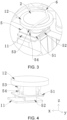
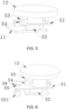
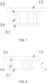
- the connection mechanism 5 comprises a moving plate 51, at least one upper connection portion 53 and at least one lower connection portion 54.
- the moving plate 51 is movably arranged on the fixed base 11 by means of a sliding rail 52, that is, the moving plate 51 is able to slide with respect to the fixed base 11 in the plane where the X-axis and the Y-axis are located by means of the sliding rail 52, wherein the realization of the function of the sliding rail 52 belongs to the prior art and will not be repeated anymore.
- the upper connection portion 53 is arranged on the wafer loader 12. Specifically, in this embodiment, the upper connection portion 53 is arranged on a lower surface of the wafer loader 12.
- connection portion 53 may be arranged at other positions of the wafer loader 12.
- the lower connection portion 54 is arranged on the moving plate 51. Specifically, in this embodiment, the lower connection portion 54 is arranged on an upper surface of the moving plate 51. Of course, in other embodiments, the lower connection portion 54 may be arranged at other positions of the moving plate 51.
- the moving plate 51 is able to move in the plane where the X-axis and the Y-axis are located, to drive the wafer loader 12 to move to the target position by means of an axial connection of the lower connection portion 54 and the upper connection portion 53.
- the upper connection portion 53 at least comprises a first section 531 and a second section 532 which are arranged coaxially, wherein the inner diameter of the first section 531 matches the outer diameter of the lower connection portion 54, that is, the inner diameter of the first section 531 is equal to the outer diameter of the lower connection portion 54 in a case where the lower connection portion 54 is cylindrical.
- the inner diameter of the second section 532 is greater than the inner diameter of the first section 531, and the second section 532 is close to the lower connection portion 54.
- a top end of the lower connection portion 54 is cut into a conical surface 541, and a necking section 533 is formed between the first section 531 and the second section 532.
- the necking section 533 may function as the second section 532 as long as the inner diameter of the necking section 533 is greater than the inner diameter of the first section 531 to ensure that the lower connection portion 54 can be smoothly inserted into the necking section 533.
- the structure of the upper connection portion and the structure of the lower connection portion can be exchanged. That is, the lower connection portion at least comprises a first section and a second section which are arranged coaxially, the inner diameter of the first section matches the outer diameter of the upper connection portion, the inner diameter of the second section is greater than the inner diameter of the first section, and the second section is close to the upper connection portion.
- the wafer loader 12 has a micro-motion state where the wafer loader 12 at least can float in the X-axis direction and the Y-axis direction.
- the wafer loader 12 in the micro-motion state is limited with respect to the fixed base 11 by means of the connection mechanism 5, thus being switched from the micro-motion state to a stationary state.
- the fixed base 11 and the wafer loader 12 can move slightly with respect to each other although they are connected by means of an existing structure.
- the wafer loader 12 will not move at least with respect to the connection mechanism 5.
- connection mechanism 5 can move with respect to the fixed base 11 by means of an external force.
- a slot 56 is formed in the moving plate 51, and an eccentric cam 55 connected to a motor 551 stretches into the slot 56 and is tangent to an inner wall of the slot 56.
- the outer diameter of the eccentric cam 55 is equal to the width of the slot 56
- the length of the slot 56 is greater than the outer diameter of the eccentric cam 55
- the axis of an output shaft of the motor 551 is located at a point A
- a tangent point of the eccentric cam 55 and the slot 56 is located on a normal B
- a deviation between A and B is in the X-axis direction.
- the position of the motor 551 is fixed relatively.
- the moving plate 51 moves along the sliding rail 52 in the plane where the X-axis and the Y-axis are located, particularly in the X-axis direction.
- the moving plate 51 can be stopped freely within the movement range by controlling the rotation angle of the motor 551.
- the wafer polishing system further comprises a storage unit used for storing rotation angles of eccentric cam 55 at different stations, such that the eccentric cam 55 can quickly rotate to a target position according to data recorded in the storage unit.
- a storage unit used for storing rotation angles of eccentric cam 55 at different stations, such that the eccentric cam 55 can quickly rotate to a target position according to data recorded in the storage unit.
- one portion of the connection mechanism 5 moves first in the plane where the X-axis and the Y-axis are located, and after the position of the connection mechanism 5 and the position of the fixed base 11 are fixed relatively, the two portions of the connection mechanism 5 are connected to allow the wafer loader 12 to move the target position, that is, the moving plate 51 is moved to the target position by means of the storage unit, and then the two portions of the connection mechanism 5 are connected.
- the clamping jaws can be automatically adjusted at different positions, and one wafer loader can correspond to multiple clamping jaws.
- the target position of the wafer loader 12 is the position exactly opposite to the clamping jaws of the clamping mechanism 6, because the existing clamping jaws 6 can only move horizontally in the X-axis direction and ascend and descend in the Z-axis direction and cannot move in the Y-axis direction, two stations are arranged in the Z-axis direction; when located at the upper station, the clamping jaws can move in the X-axis direction to transfer the wafer to different areas; and when located at the lower station, the clamping jaws can pick up the wafer from the wafer loader or place the wafer onto the wafer loader.
- At least two clamping jaws 6 are arranged, at least one clamping jaw is used for picking and placing non-polished wafers, and at least one clamping jaw is used for picking and placing polished wafers, that is, a placement clamping jaw is used for placing a to-be-polished wafer on the wafer loader, and a pick-up clamping jaw is used for taking the polished wafer from the wafer loader, and the two clamping jaws are located on two sides of the wafer transfer channel 3 respectively.
- one clamping jaw 6 may be arranged.
- a loading method for a wafer polishing system is implemented based on the structure of the above wafer polishing system and comprises:
- the loading method for a wafer polishing system is implemented based on the structure of the above wafer polishing system and comprises:
- the loading method for a wafer polishing system is specifically described below with reference to three embodiments.
- the loading method for a wafer polishing system is implemented based on the structure of the above wafer polishing system and comprises the following steps:
- the motion time for the whole connection process is short, and the time efficiency is high.
- the loading method for a wafer polishing system is implemented based on the structure of the above wafer polishing system and comprises the following steps:
- the requirement for the structural design is low, and the position of the wafer loader 12 can be adjusted only by moving the moving plate 51 by means of an external force.
- the wafer loader 12 starts to ascend or descend in the Z-axis direction to be close to the fixed base 11, wherein this movement is defined as a motion B;
- connection mechanisms have been connected and limited before the moving plate 51 moves, such that the moving plate 51 and the wafer loader 12 can be driven to move as a hole by means of an external force.
- the wafer polishing system and the loading method therefor are applied to a specific usage scenario, that is, a using method for a wafer polishing system is implemented based on the structure of the above wafer polishing system and the loading method, and comprises:
- the application of this embodiment can eliminate various inevitable errors generated in the production and assembly process of polishing equipment to solve the problem that the clamping jaw 6 and the wafer loader 12 are in different matching states in the X-axis direction and the Y-axis direction, particularly in the Y-axis direction, when the clamping jaw 6 picks up or places the wafer 2 on the wafer loader 12 at different positions in the X-axis direction due to unparallel movement paths of the fixed base 11 in the X-axis direction.
- FIG. 11 the application of this embodiment can eliminate various inevitable errors generated in the production and assembly process of polishing equipment to solve the problem that the clamping jaw 6 and the wafer loader 12 are in different matching states in the X-axis direction and the Y-axis direction, particularly in the Y-axis direction, when the clamping jaw 6 picks up or places the wafer 2 on the wafer loader 12 at different positions in the X-axis direction due to unparallel movement paths of the fixed base 11 in the X-axis direction
- the desired wafer pickup and placement position is position d
- the actual wafer pickup and placement position caused by errors is position e
- there is a deviation ⁇ y between the desired wafer pickup and placement position and the actual wafer pickup and placement position in the Y-axis direction and this embodiment eliminates the deviation ⁇ y and realizes accurate matching between the clamping jaw 6 and the wafer loader 12.
- the using method for a wafer polishing system comprises the following steps:
- the using method for a wafer polishing system comprises the following steps:
- the using method for a wafer polishing system comprises the following steps:
Landscapes
- Engineering & Computer Science (AREA)
- Mechanical Engineering (AREA)
- Chemical & Material Sciences (AREA)
- Ceramic Engineering (AREA)
- Inorganic Chemistry (AREA)
- Finish Polishing, Edge Sharpening, And Grinding By Specific Grinding Devices (AREA)
- Container, Conveyance, Adherence, Positioning, Of Wafer (AREA)
- Mechanical Treatment Of Semiconductor (AREA)
- Robotics (AREA)
- Constituent Portions Of Griding Lathes, Driving, Sensing And Control (AREA)
Applications Claiming Priority (2)
| Application Number | Priority Date | Filing Date | Title |
|---|---|---|---|
| CN202210316152.7A CN114619308B (zh) | 2022-03-29 | 2022-03-29 | 一种晶圆抛光系统、装载方法及其使用方法 |
| PCT/CN2023/071166 WO2023185202A1 (fr) | 2022-03-29 | 2023-01-09 | Système de polissage de tranche, et procédé de chargement et procédé d'utilisation de celui-ci |
Publications (2)
| Publication Number | Publication Date |
|---|---|
| EP4501537A1 true EP4501537A1 (fr) | 2025-02-05 |
| EP4501537A4 EP4501537A4 (fr) | 2026-03-11 |
Family
ID=81904484
Family Applications (1)
| Application Number | Title | Priority Date | Filing Date |
|---|---|---|---|
| EP23777581.2A Pending EP4501537A4 (fr) | 2022-03-29 | 2023-01-09 | Système de polissage de tranche, et procédé de chargement et procédé d'utilisation de celui-ci |
Country Status (7)
| Country | Link |
|---|---|
| US (1) | US20250214196A1 (fr) |
| EP (1) | EP4501537A4 (fr) |
| JP (1) | JP7736360B2 (fr) |
| KR (1) | KR102816529B1 (fr) |
| CN (1) | CN114619308B (fr) |
| TW (1) | TWI823623B (fr) |
| WO (1) | WO2023185202A1 (fr) |
Families Citing this family (5)
| Publication number | Priority date | Publication date | Assignee | Title |
|---|---|---|---|---|
| CN114619308B (zh) * | 2022-03-29 | 2023-05-16 | 杭州众硅电子科技有限公司 | 一种晶圆抛光系统、装载方法及其使用方法 |
| CN115338705A (zh) * | 2022-06-30 | 2022-11-15 | 杭州众硅电子科技有限公司 | 一种连续式晶圆抛光系统 |
| CN117457569B (zh) * | 2023-10-26 | 2024-05-24 | 河北光森电子科技有限公司 | 一种晶圆载片台 |
| CN118366908B (zh) * | 2024-04-28 | 2024-11-08 | 德沪涂膜设备(苏州)有限公司 | 一种晶硅对位装置以及涂膜设备 |
| CN120170631B (zh) * | 2025-05-20 | 2025-08-19 | 华海清科(北京)科技有限公司 | 化学机械抛光设备及晶圆传输方法 |
Family Cites Families (12)
| Publication number | Priority date | Publication date | Assignee | Title |
|---|---|---|---|---|
| JPS62268136A (ja) * | 1986-05-16 | 1987-11-20 | Oki Electric Ind Co Ltd | ウエハキヤリア移載装置 |
| US8296937B2 (en) * | 2008-08-19 | 2012-10-30 | Silverbrook Research Pty Ltd | Wafer positioning system |
| CN102371535B (zh) * | 2010-08-11 | 2014-07-23 | 中国电子科技集团公司第四十五研究所 | 应用于化学机械抛光设备中的硅片定位装载装置 |
| TWI672191B (zh) * | 2013-10-16 | 2019-09-21 | Applied Materials, Inc. | 帶有裝設樞紐手臂之化學機械拋光機的系統及方法 |
| CN109015314A (zh) * | 2018-09-07 | 2018-12-18 | 杭州众硅电子科技有限公司 | 一种化学机械平坦化设备 |
| CN109304665A (zh) * | 2018-09-20 | 2019-02-05 | 杭州众硅电子科技有限公司 | 一种包含可移动装卸模块的抛光装卸部件模块 |
| JP7534084B2 (ja) * | 2019-06-18 | 2024-08-14 | 株式会社荏原製作所 | 基板保持装置および基板処理装置 |
| CN111421412B (zh) * | 2020-05-20 | 2022-03-04 | 清华大学 | 一种磨削工作台和晶圆减薄设备 |
| CN111604810B (zh) * | 2020-07-24 | 2020-11-03 | 杭州众硅电子科技有限公司 | 一种晶圆传输设备、化学机械平坦化装置及晶圆传输方法 |
| CN112476129A (zh) * | 2020-11-26 | 2021-03-12 | 乌兰 | 一种半导体多规格研磨设备 |
| CN114141685B (zh) * | 2021-11-29 | 2024-10-29 | 苏州科韵激光科技有限公司 | 一种自动化晶圆载台及其使用方法 |
| CN114619308B (zh) * | 2022-03-29 | 2023-05-16 | 杭州众硅电子科技有限公司 | 一种晶圆抛光系统、装载方法及其使用方法 |
-
2022
- 2022-03-29 CN CN202210316152.7A patent/CN114619308B/zh active Active
- 2022-10-17 TW TW111139192A patent/TWI823623B/zh active
-
2023
- 2023-01-09 KR KR1020247024097A patent/KR102816529B1/ko active Active
- 2023-01-09 US US18/848,126 patent/US20250214196A1/en active Pending
- 2023-01-09 EP EP23777581.2A patent/EP4501537A4/fr active Pending
- 2023-01-09 WO PCT/CN2023/071166 patent/WO2023185202A1/fr not_active Ceased
- 2023-01-09 JP JP2024557232A patent/JP7736360B2/ja active Active
Also Published As
| Publication number | Publication date |
|---|---|
| WO2023185202A1 (fr) | 2023-10-05 |
| US20250214196A1 (en) | 2025-07-03 |
| TWI823623B (zh) | 2023-11-21 |
| KR102816529B1 (ko) | 2025-06-02 |
| KR20240118176A (ko) | 2024-08-02 |
| JP7736360B2 (ja) | 2025-09-09 |
| CN114619308B (zh) | 2023-05-16 |
| TW202339074A (zh) | 2023-10-01 |
| JP2025510300A (ja) | 2025-04-14 |
| CN114619308A (zh) | 2022-06-14 |
| EP4501537A4 (fr) | 2026-03-11 |
Similar Documents
| Publication | Publication Date | Title |
|---|---|---|
| EP4501537A1 (fr) | Système de polissage de tranche, et procédé de chargement et procédé d'utilisation de celui-ci | |
| US12230515B2 (en) | Substrate processing apparatus and substrate processing method | |
| KR102050004B1 (ko) | 실리콘 웨이퍼 이송 시스템 | |
| CN116153820A (zh) | 一种多类型芯片全自动混合贴装设备及贴装方法 | |
| US20110215134A1 (en) | Rotary die bonding apparatus and methodology thereof | |
| CN114261751A (zh) | 一种晶圆上下料系统及上下料方法 | |
| US9931730B2 (en) | Automatic handling apparatus with positioning pins | |
| WO2018032656A1 (fr) | Dispositif de saisie et de placement de composant à grande vitesse | |
| CN1771580A (zh) | 在清洁模块之间垂直传送半导体基板的方法和设备 | |
| JP5027210B2 (ja) | 電子構成要素、詳細には半導体チップを基板に配置するための方法および装置 | |
| CN116021392A (zh) | 晶圆倒角加工全自动设备 | |
| WO2020056818A1 (fr) | Module de composant de chargement et de déchargement de polissage contenant un module mobile de chargement et de déchargement | |
| KR20050092415A (ko) | 전자부품 실장장치 및 전자부품 실장방법 | |
| JP3497078B2 (ja) | ダイボンダ | |
| CN218887149U (zh) | 晶片装载装置 | |
| CN110970321A (zh) | 一种芯片贴片设备及芯片贴片方法 | |
| CN117116783A (zh) | 一种高精度环氧贴片机及快速贴片方法 | |
| JP2001319938A (ja) | チップ移送装置 | |
| CN221805480U (zh) | 晶圆加工机构及其晶圆上下料机构 | |
| CN114121722A (zh) | 微型发光二极管巨量转移装置 | |
| JP2004179523A (ja) | 電子部品実装装置 | |
| CN117637576A (zh) | 加工装置 | |
| CN217534475U (zh) | 一种晶圆传递装置 | |
| JPH09148395A (ja) | 基板搬送装置 | |
| CN222830938U (zh) | 激光加工设备 |
Legal Events
| Date | Code | Title | Description |
|---|---|---|---|
| STAA | Information on the status of an ep patent application or granted ep patent |
Free format text: STATUS: THE INTERNATIONAL PUBLICATION HAS BEEN MADE |
|
| PUAI | Public reference made under article 153(3) epc to a published international application that has entered the european phase |
Free format text: ORIGINAL CODE: 0009012 |
|
| STAA | Information on the status of an ep patent application or granted ep patent |
Free format text: STATUS: REQUEST FOR EXAMINATION WAS MADE |
|
| 17P | Request for examination filed |
Effective date: 20240924 |
|
| AK | Designated contracting states |
Kind code of ref document: A1 Designated state(s): AL AT BE BG CH CY CZ DE DK EE ES FI FR GB GR HR HU IE IS IT LI LT LU LV MC ME MK MT NL NO PL PT RO RS SE SI SK SM TR |
|
| DAV | Request for validation of the european patent (deleted) | ||
| DAX | Request for extension of the european patent (deleted) | ||
| A4 | Supplementary search report drawn up and despatched |
Effective date: 20260210 |
|
| RIC1 | Information provided on ipc code assigned before grant |
Ipc: B24B 7/22 20060101AFI20260204BHEP Ipc: B24B 41/06 20120101ALI20260204BHEP Ipc: B65G 47/52 20060101ALI20260204BHEP Ipc: B24B 27/00 20060101ALI20260204BHEP Ipc: B24B 37/04 20120101ALI20260204BHEP Ipc: B24B 37/34 20120101ALI20260204BHEP |