EP4501617A1 - Corps multicouche optique et procédé de production de corps multicouche optique - Google Patents
Corps multicouche optique et procédé de production de corps multicouche optique Download PDFInfo
- Publication number
- EP4501617A1 EP4501617A1 EP23779119.9A EP23779119A EP4501617A1 EP 4501617 A1 EP4501617 A1 EP 4501617A1 EP 23779119 A EP23779119 A EP 23779119A EP 4501617 A1 EP4501617 A1 EP 4501617A1
- Authority
- EP
- European Patent Office
- Prior art keywords
- layer
- sensitive adhesive
- pressure
- porous layer
- porous
- Prior art date
- Legal status (The legal status is an assumption and is not a legal conclusion. Google has not performed a legal analysis and makes no representation as to the accuracy of the status listed.)
- Pending
Links
Images
Classifications
-
- C—CHEMISTRY; METALLURGY
- C09—DYES; PAINTS; POLISHES; NATURAL RESINS; ADHESIVES; COMPOSITIONS NOT OTHERWISE PROVIDED FOR; APPLICATIONS OF MATERIALS NOT OTHERWISE PROVIDED FOR
- C09J—ADHESIVES; NON-MECHANICAL ASPECTS OF ADHESIVE PROCESSES IN GENERAL; ADHESIVE PROCESSES NOT PROVIDED FOR ELSEWHERE; USE OF MATERIALS AS ADHESIVES
- C09J7/00—Adhesives in the form of films or foils
- C09J7/30—Adhesives in the form of films or foils characterised by the adhesive composition
- C09J7/38—Pressure-sensitive adhesives [PSA]
-
- B—PERFORMING OPERATIONS; TRANSPORTING
- B32—LAYERED PRODUCTS
- B32B—LAYERED PRODUCTS, i.e. PRODUCTS BUILT-UP OF STRATA OF FLAT OR NON-FLAT, e.g. CELLULAR OR HONEYCOMB, FORM
- B32B3/00—Layered products comprising a layer with external or internal discontinuities or unevennesses, or a layer of non-planar shape; Layered products comprising a layer having particular features of form
- B32B3/10—Layered products comprising a layer with external or internal discontinuities or unevennesses, or a layer of non-planar shape; Layered products comprising a layer having particular features of form characterised by a discontinuous layer, i.e. formed of separate pieces of material
-
- C—CHEMISTRY; METALLURGY
- C09—DYES; PAINTS; POLISHES; NATURAL RESINS; ADHESIVES; COMPOSITIONS NOT OTHERWISE PROVIDED FOR; APPLICATIONS OF MATERIALS NOT OTHERWISE PROVIDED FOR
- C09J—ADHESIVES; NON-MECHANICAL ASPECTS OF ADHESIVE PROCESSES IN GENERAL; ADHESIVE PROCESSES NOT PROVIDED FOR ELSEWHERE; USE OF MATERIALS AS ADHESIVES
- C09J7/00—Adhesives in the form of films or foils
- C09J7/20—Adhesives in the form of films or foils characterised by their carriers
- C09J7/29—Laminated material
-
- B—PERFORMING OPERATIONS; TRANSPORTING
- B32—LAYERED PRODUCTS
- B32B—LAYERED PRODUCTS, i.e. PRODUCTS BUILT-UP OF STRATA OF FLAT OR NON-FLAT, e.g. CELLULAR OR HONEYCOMB, FORM
- B32B5/00—Layered products characterised by the non- homogeneity or physical structure, i.e. comprising a fibrous, filamentary, particulate or foam layer; Layered products characterised by having a layer differing constitutionally or physically in different parts
- B32B5/18—Layered products characterised by the non- homogeneity or physical structure, i.e. comprising a fibrous, filamentary, particulate or foam layer; Layered products characterised by having a layer differing constitutionally or physically in different parts characterised by features of a layer of foamed material
-
- B—PERFORMING OPERATIONS; TRANSPORTING
- B32—LAYERED PRODUCTS
- B32B—LAYERED PRODUCTS, i.e. PRODUCTS BUILT-UP OF STRATA OF FLAT OR NON-FLAT, e.g. CELLULAR OR HONEYCOMB, FORM
- B32B7/00—Layered products characterised by the relation between layers; Layered products characterised by the relative orientation of features between layers, or by the relative values of a measurable parameter between layers, i.e. products comprising layers having different physical, chemical or physicochemical properties; Layered products characterised by the interconnection of layers
- B32B7/02—Physical, chemical or physicochemical properties
- B32B7/023—Optical properties
-
- C—CHEMISTRY; METALLURGY
- C09—DYES; PAINTS; POLISHES; NATURAL RESINS; ADHESIVES; COMPOSITIONS NOT OTHERWISE PROVIDED FOR; APPLICATIONS OF MATERIALS NOT OTHERWISE PROVIDED FOR
- C09J—ADHESIVES; NON-MECHANICAL ASPECTS OF ADHESIVE PROCESSES IN GENERAL; ADHESIVE PROCESSES NOT PROVIDED FOR ELSEWHERE; USE OF MATERIALS AS ADHESIVES
- C09J7/00—Adhesives in the form of films or foils
- C09J7/20—Adhesives in the form of films or foils characterised by their carriers
- C09J7/22—Plastics; Metallised plastics
-
- G—PHYSICS
- G02—OPTICS
- G02B—OPTICAL ELEMENTS, SYSTEMS OR APPARATUS
- G02B6/00—Light guides; Structural details of arrangements comprising light guides and other optical elements, e.g. couplings
- G02B6/0001—Light guides; Structural details of arrangements comprising light guides and other optical elements, e.g. couplings specially adapted for lighting devices or systems
- G02B6/0011—Light guides; Structural details of arrangements comprising light guides and other optical elements, e.g. couplings specially adapted for lighting devices or systems the light guides being planar or of plate-like form
- G02B6/0033—Means for improving the coupling-out of light from the light guide
- G02B6/005—Means for improving the coupling-out of light from the light guide provided by one optical element, or plurality thereof, placed on the light output side of the light guide
-
- G—PHYSICS
- G02—OPTICS
- G02B—OPTICAL ELEMENTS, SYSTEMS OR APPARATUS
- G02B6/00—Light guides; Structural details of arrangements comprising light guides and other optical elements, e.g. couplings
- G02B6/0001—Light guides; Structural details of arrangements comprising light guides and other optical elements, e.g. couplings specially adapted for lighting devices or systems
- G02B6/0011—Light guides; Structural details of arrangements comprising light guides and other optical elements, e.g. couplings specially adapted for lighting devices or systems the light guides being planar or of plate-like form
- G02B6/0033—Means for improving the coupling-out of light from the light guide
- G02B6/0058—Means for improving the coupling-out of light from the light guide varying in density, size, shape or depth along the light guide
- G02B6/0061—Means for improving the coupling-out of light from the light guide varying in density, size, shape or depth along the light guide to provide homogeneous light output intensity
-
- G—PHYSICS
- G02—OPTICS
- G02B—OPTICAL ELEMENTS, SYSTEMS OR APPARATUS
- G02B6/00—Light guides; Structural details of arrangements comprising light guides and other optical elements, e.g. couplings
- G02B6/0001—Light guides; Structural details of arrangements comprising light guides and other optical elements, e.g. couplings specially adapted for lighting devices or systems
- G02B6/0011—Light guides; Structural details of arrangements comprising light guides and other optical elements, e.g. couplings specially adapted for lighting devices or systems the light guides being planar or of plate-like form
- G02B6/0065—Manufacturing aspects; Material aspects
-
- G—PHYSICS
- G02—OPTICS
- G02B—OPTICAL ELEMENTS, SYSTEMS OR APPARATUS
- G02B6/00—Light guides; Structural details of arrangements comprising light guides and other optical elements, e.g. couplings
- G02B6/0001—Light guides; Structural details of arrangements comprising light guides and other optical elements, e.g. couplings specially adapted for lighting devices or systems
- G02B6/0011—Light guides; Structural details of arrangements comprising light guides and other optical elements, e.g. couplings specially adapted for lighting devices or systems the light guides being planar or of plate-like form
- G02B6/0081—Mechanical or electrical aspects of the light guide and light source in the lighting device peculiar to the adaptation to planar light guides, e.g. concerning packaging
- G02B6/0086—Positioning aspects
- G02B6/0088—Positioning aspects of the light guide or other optical sheets in the package
-
- B—PERFORMING OPERATIONS; TRANSPORTING
- B32—LAYERED PRODUCTS
- B32B—LAYERED PRODUCTS, i.e. PRODUCTS BUILT-UP OF STRATA OF FLAT OR NON-FLAT, e.g. CELLULAR OR HONEYCOMB, FORM
- B32B2307/00—Properties of the layers or laminate
- B32B2307/40—Properties of the layers or laminate having particular optical properties
- B32B2307/412—Transparent
-
- B—PERFORMING OPERATIONS; TRANSPORTING
- B32—LAYERED PRODUCTS
- B32B—LAYERED PRODUCTS, i.e. PRODUCTS BUILT-UP OF STRATA OF FLAT OR NON-FLAT, e.g. CELLULAR OR HONEYCOMB, FORM
- B32B2307/00—Properties of the layers or laminate
- B32B2307/40—Properties of the layers or laminate having particular optical properties
- B32B2307/414—Translucent
-
- B—PERFORMING OPERATIONS; TRANSPORTING
- B32—LAYERED PRODUCTS
- B32B—LAYERED PRODUCTS, i.e. PRODUCTS BUILT-UP OF STRATA OF FLAT OR NON-FLAT, e.g. CELLULAR OR HONEYCOMB, FORM
- B32B2307/00—Properties of the layers or laminate
- B32B2307/40—Properties of the layers or laminate having particular optical properties
- B32B2307/418—Refractive
-
- C—CHEMISTRY; METALLURGY
- C09—DYES; PAINTS; POLISHES; NATURAL RESINS; ADHESIVES; COMPOSITIONS NOT OTHERWISE PROVIDED FOR; APPLICATIONS OF MATERIALS NOT OTHERWISE PROVIDED FOR
- C09J—ADHESIVES; NON-MECHANICAL ASPECTS OF ADHESIVE PROCESSES IN GENERAL; ADHESIVE PROCESSES NOT PROVIDED FOR ELSEWHERE; USE OF MATERIALS AS ADHESIVES
- C09J2301/00—Additional features of adhesives in the form of films or foils
- C09J2301/10—Additional features of adhesives in the form of films or foils characterized by the structural features of the adhesive tape or sheet
- C09J2301/12—Additional features of adhesives in the form of films or foils characterized by the structural features of the adhesive tape or sheet by the arrangement of layers
- C09J2301/124—Additional features of adhesives in the form of films or foils characterized by the structural features of the adhesive tape or sheet by the arrangement of layers the adhesive layer being present on both sides of the carrier, e.g. double-sided adhesive tape
- C09J2301/1242—Additional features of adhesives in the form of films or foils characterized by the structural features of the adhesive tape or sheet by the arrangement of layers the adhesive layer being present on both sides of the carrier, e.g. double-sided adhesive tape the opposite adhesive layers being different
-
- C—CHEMISTRY; METALLURGY
- C09—DYES; PAINTS; POLISHES; NATURAL RESINS; ADHESIVES; COMPOSITIONS NOT OTHERWISE PROVIDED FOR; APPLICATIONS OF MATERIALS NOT OTHERWISE PROVIDED FOR
- C09J—ADHESIVES; NON-MECHANICAL ASPECTS OF ADHESIVE PROCESSES IN GENERAL; ADHESIVE PROCESSES NOT PROVIDED FOR ELSEWHERE; USE OF MATERIALS AS ADHESIVES
- C09J2301/00—Additional features of adhesives in the form of films or foils
- C09J2301/10—Additional features of adhesives in the form of films or foils characterized by the structural features of the adhesive tape or sheet
- C09J2301/16—Additional features of adhesives in the form of films or foils characterized by the structural features of the adhesive tape or sheet by the structure of the carrier layer
-
- C—CHEMISTRY; METALLURGY
- C09—DYES; PAINTS; POLISHES; NATURAL RESINS; ADHESIVES; COMPOSITIONS NOT OTHERWISE PROVIDED FOR; APPLICATIONS OF MATERIALS NOT OTHERWISE PROVIDED FOR
- C09J—ADHESIVES; NON-MECHANICAL ASPECTS OF ADHESIVE PROCESSES IN GENERAL; ADHESIVE PROCESSES NOT PROVIDED FOR ELSEWHERE; USE OF MATERIALS AS ADHESIVES
- C09J2301/00—Additional features of adhesives in the form of films or foils
- C09J2301/30—Additional features of adhesives in the form of films or foils characterized by the chemical, physicochemical or physical properties of the adhesive or the carrier
- C09J2301/312—Additional features of adhesives in the form of films or foils characterized by the chemical, physicochemical or physical properties of the adhesive or the carrier parameters being the characterizing feature
-
- C—CHEMISTRY; METALLURGY
- C09—DYES; PAINTS; POLISHES; NATURAL RESINS; ADHESIVES; COMPOSITIONS NOT OTHERWISE PROVIDED FOR; APPLICATIONS OF MATERIALS NOT OTHERWISE PROVIDED FOR
- C09J—ADHESIVES; NON-MECHANICAL ASPECTS OF ADHESIVE PROCESSES IN GENERAL; ADHESIVE PROCESSES NOT PROVIDED FOR ELSEWHERE; USE OF MATERIALS AS ADHESIVES
- C09J2301/00—Additional features of adhesives in the form of films or foils
- C09J2301/50—Additional features of adhesives in the form of films or foils characterized by process specific features
-
- C—CHEMISTRY; METALLURGY
- C09—DYES; PAINTS; POLISHES; NATURAL RESINS; ADHESIVES; COMPOSITIONS NOT OTHERWISE PROVIDED FOR; APPLICATIONS OF MATERIALS NOT OTHERWISE PROVIDED FOR
- C09J—ADHESIVES; NON-MECHANICAL ASPECTS OF ADHESIVE PROCESSES IN GENERAL; ADHESIVE PROCESSES NOT PROVIDED FOR ELSEWHERE; USE OF MATERIALS AS ADHESIVES
- C09J2400/00—Presence of inorganic and organic materials
- C09J2400/10—Presence of inorganic materials
-
- C—CHEMISTRY; METALLURGY
- C09—DYES; PAINTS; POLISHES; NATURAL RESINS; ADHESIVES; COMPOSITIONS NOT OTHERWISE PROVIDED FOR; APPLICATIONS OF MATERIALS NOT OTHERWISE PROVIDED FOR
- C09J—ADHESIVES; NON-MECHANICAL ASPECTS OF ADHESIVE PROCESSES IN GENERAL; ADHESIVE PROCESSES NOT PROVIDED FOR ELSEWHERE; USE OF MATERIALS AS ADHESIVES
- C09J2400/00—Presence of inorganic and organic materials
- C09J2400/20—Presence of organic materials
- C09J2400/24—Presence of a foam
- C09J2400/243—Presence of a foam in the substrate
-
- C—CHEMISTRY; METALLURGY
- C09—DYES; PAINTS; POLISHES; NATURAL RESINS; ADHESIVES; COMPOSITIONS NOT OTHERWISE PROVIDED FOR; APPLICATIONS OF MATERIALS NOT OTHERWISE PROVIDED FOR
- C09J—ADHESIVES; NON-MECHANICAL ASPECTS OF ADHESIVE PROCESSES IN GENERAL; ADHESIVE PROCESSES NOT PROVIDED FOR ELSEWHERE; USE OF MATERIALS AS ADHESIVES
- C09J2429/00—Presence of polyvinyl alcohol
- C09J2429/006—Presence of polyvinyl alcohol in the substrate
-
- C—CHEMISTRY; METALLURGY
- C09—DYES; PAINTS; POLISHES; NATURAL RESINS; ADHESIVES; COMPOSITIONS NOT OTHERWISE PROVIDED FOR; APPLICATIONS OF MATERIALS NOT OTHERWISE PROVIDED FOR
- C09J—ADHESIVES; NON-MECHANICAL ASPECTS OF ADHESIVE PROCESSES IN GENERAL; ADHESIVE PROCESSES NOT PROVIDED FOR ELSEWHERE; USE OF MATERIALS AS ADHESIVES
- C09J2433/00—Presence of (meth)acrylic polymer
-
- C—CHEMISTRY; METALLURGY
- C09—DYES; PAINTS; POLISHES; NATURAL RESINS; ADHESIVES; COMPOSITIONS NOT OTHERWISE PROVIDED FOR; APPLICATIONS OF MATERIALS NOT OTHERWISE PROVIDED FOR
- C09J—ADHESIVES; NON-MECHANICAL ASPECTS OF ADHESIVE PROCESSES IN GENERAL; ADHESIVE PROCESSES NOT PROVIDED FOR ELSEWHERE; USE OF MATERIALS AS ADHESIVES
- C09J2433/00—Presence of (meth)acrylic polymer
- C09J2433/006—Presence of (meth)acrylic polymer in the substrate
-
- C—CHEMISTRY; METALLURGY
- C09—DYES; PAINTS; POLISHES; NATURAL RESINS; ADHESIVES; COMPOSITIONS NOT OTHERWISE PROVIDED FOR; APPLICATIONS OF MATERIALS NOT OTHERWISE PROVIDED FOR
- C09J—ADHESIVES; NON-MECHANICAL ASPECTS OF ADHESIVE PROCESSES IN GENERAL; ADHESIVE PROCESSES NOT PROVIDED FOR ELSEWHERE; USE OF MATERIALS AS ADHESIVES
- C09J2483/00—Presence of polysiloxane
- C09J2483/006—Presence of polysiloxane in the substrate
Definitions
- the present invention relates to an optical laminate and a method of producing an optical laminate.
- an optical laminate including: a substrate; and a variable refractive index extraction layer arranged on the substrate, wherein the variable refractive index extraction layer includes a first region where a first substance having a relatively low refractive index is selectively printed, and a second region formed by overcoating the first substance with a second substance having a relatively high refractive index (see, for example, Patent Literature 1).
- the optical laminate described in Patent Literature 1 is bonded to a light guide plate via a pressure-sensitive adhesive layer, the pressure-sensitive adhesive layer being formed on the surface of the substrate opposite to the variable refractive index extraction layer.
- the present invention has been made to solve the above-mentioned problem of the related art, and a primary object of the present invention is to provide an optical laminate that can be reduced in thickness and that can maintain excellent optical performance, and a method of producing the optical laminate.
- an optical laminate including: a transparent layer having a thickness of 20 um or less; a porous layer directly arranged in a predetermined pattern on one surface of the transparent layer in a thickness direction, the porous layer having a refractive index of 1.25 or less; an adhesion layer arranged on a side of the transparent layer opposite to the porous layer, the adhesion layer being brought into contact with the transparent layer; and a pressure-sensitive adhesive layer arranged on a side of the transparent layer opposite to the adhesion layer, the pressure-sensitive adhesive layer covering the porous layer.
- the transparent layer has a barrier function for suppressing a component for forming the adhesion layer from permeating through the porous layer.
- a porosity of the transparent layer is lower than a porosity of the porous layer.
- the pressure-sensitive adhesive layer includes a pressure-sensitive adhesive having a storage modulus of elasticity at 23°C of 1.0 ⁇ 10 5 (Pa) or more.
- a method of producing an optical laminate including the steps of: forming a transparent layer having a thickness of 20 um or less on a substrate; forming a porous layer having a refractive index of 1.25 or less in a pattern on a surface of the transparent layer opposite to the substrate; forming a pressure-sensitive adhesive layer so as to cover the porous layer from a side of the porous layer opposite to the transparent layer; peeling the substrate from the transparent layer; and forming an adhesion layer on a surface of the transparent layer opposite to the porous layer.
- a peel strength when the substrate is peeled from the transparent layer is 1 N/25 mm or less.
- the optical laminate that can be reduced in thickness and that can maintain excellent optical performance can be achieved.
- Embodiments of the present invention are described below. However, the present invention is not limited to these embodiments. First, the outline of the overall configuration of an optical laminate is described. Next, constituents of the optical laminate are specifically described.
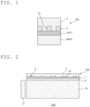
- FIG. 1 is a schematic sectional view of an optical laminate according to one embodiment of the present invention.
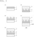
- FIG. 2 is a schematic sectional view of an optical product including the optical laminate of FIG. 1 .
- An optical laminate 100 of the illustrated example includes: a transparent layer 1 having a thickness of 20 um or less; a porous layer 2 directly arranged in a predetermined pattern on one surface of the transparent layer 1 in a thickness direction, the porous layer 2 having a refractive index of 1.25 or less; an adhesion layer 4 arranged on a side of the transparent layer 1 opposite to the porous layer 2, the adhesion layer 4 being brought into contact with the transparent layer 1; and a pressure-sensitive adhesive layer 3 arranged on a side of the transparent layer 1 opposite to the adhesion layer 4, the pressure-sensitive adhesive layer 3 covering the porous layer 2.
- Such configuration can reduce the thickness of the optical laminate and maintain the refractive index of the porous layer to the above-mentioned upper limit or less because the transparent layer is arranged between the porous layer and the adhesion layer, and the transparent layer has a thickness of 20 um or less. Accordingly, excellent optical performance of the optical laminate can be sufficiently maintained.
- the thickness of the transparent layer 1 is preferably 10 um or less, more preferably 5 um or less, still more preferably 4 um or less, and is typically 0.1 um or more.
- the porous layer 2 typically has pores therein.
- the refractive index of the porous layer 2 is preferably less than 1.20, more preferably 1.19 or less, still more preferably 1.18 or less, and is typically 1.10 or more.
- the refractive index refers to a refractive index measured at a wavelength of 550 nm unless otherwise stated.
- part of the one surface of the transparent layer 1 in the thickness direction may be exposed through the porous layer 2.
- the exposed portion is brought into contact with the pressure-sensitive adhesive layer 3.
- the pressure-sensitive adhesive layer 3 is brought into contact with the porous layer 2 and the transparent layer 1.
- the refractive index of the pressure-sensitive adhesive layer 3 is typically higher than the refractive index of the porous layer 2.
- the refractive index of the pressure-sensitive adhesive layer 3 is more than 1.25, preferably 1.4 or more, and is typically 1.7 or less.
- the transparent layer 1 is a barrier layer 1a having a barrier function for suppressing a component for forming the adhesion layer 4 from permeating through the porous layer 2. Accordingly, the transparent layer 1 can stably suppress an increase in refractive index of the porous layer.
- the adhesion layer 4 may be a pressure-sensitive adhesive layer or an adhesive layer.
- the porosity of the transparent layer 1 is lower than the porosity of the porous layer 2.
- Such configuration can sufficiently secure the barrier performance of the transparent layer 1, and stably suppress a pressure-sensitive adhesive or adhesive for forming the adhesion layer from entering the pores of the porous layer.
- the porosity of the transparent layer 1 is, for example, 15 vol% or less, preferably 10 vol% or less, and the lower limit thereof is, for example, 1 vol% or more.
- the porosity of the porous layer 2 is, for example, more than 10 vol%, preferably 20 vol% or more, more preferably 30 vol% or more, still more preferably 35 vol% or more, and is, for example, 60 vol% or less, preferably 55 vol% or less, more preferably 50 vol% or less, still more preferably 45 vol% or less.
- the refractive index of the porous layer can be set within an appropriate range, and a predetermined mechanical strength can be secured.
- the porosity is a value calculated from the value of the refractive index measured with an ellipsometer by using Lorentz-Lorenz's formula.
- the pressure-sensitive adhesive layer 3 includes a pressure-sensitive adhesive having a storage modulus of elasticity at 23°C of 1.0 ⁇ 10 5 (Pa) or more.
- the storage modulus of elasticity at 23°C of the pressure-sensitive adhesive for forming the pressure-sensitive adhesive layer 3 is preferably 1.1 ⁇ 10 5 (Pa) or more, more preferably 1.2 ⁇ 10 5 (Pa) or more.
- the pressure-sensitive adhesive for forming the pressure-sensitive adhesive layer can be suppressed from entering the pores of the porous layer. Accordingly, an increase in refractive index of the porous layer can be more stably suppressed.
- the storage modulus of elasticity is determined by reading a value at 23°C at the time of measurement in conformity with a method described in JIS K 7244-1 "Plastics-Determination of dynamic mechanical properties" under the condition of a frequency of 1 Hz in the range of from -50°C to 150°C at a rate of temperature increase of 5°C/min.
- the upper limit of the storage modulus of elasticity at 23°C of the pressure-sensitive adhesive for forming the pressure-sensitive adhesive layer 3 is typically 100 ⁇ 10 5 (Pa) or less.
- the transparent layer, the porous layer, the adhesion layer, and the pressure-sensitive adhesive layer are specifically described below.
- the transparent layer 1 can transmit light.
- the total light transmittance of the transparent layer 1 is, for example, from 70% to 100%, preferably from 80% to 99%.
- excellent transparency can be achieved in the entirety of the optical laminate. As a result, adverse effects in the applications of the optical laminate can be suppressed.
- the transparent layer 1 examples include a resin film and an inorganic thin film.
- a material for the resin film include: polyvinyl alcohol (PVA); a (meth)acrylic resin such as polymethyl methacrylate (PMMA); a polyvinyl acetal resin; a thermoplastic resin material having a polar group, such as a polycarbonate resin, a polyarylate resin, or a polyurethanebased resin; and a thermally or UV-curable resin material, such as an acrylic hard coat resin material, an epoxy-based hard coat resin material, or a silicone-based hard coat resin material.
- (meth)acrylic refers to acrylic and/or methacrylic.
- the materials for the resin film may be used alone or in combination thereof.
- the resin film may be formed of a resin composition alone, or any other substance may be added to change the physical properties of the resin film. Specifically, for example, a boric acid compound or a silanebased compound is added to introduce a cross-linking structure into PVA.
- Examples of a material for the inorganic thin film include SiO 2 , ZTO, ITO, IZO, TiO 2 , Si, ZnO, AZO, Al 2 O 3 , MgO, MgF 2 , and SiN.
- the materials for the inorganic thin film may be used alone or in combination thereof.
- the porous layer 2 is directly arranged on the one surface of the transparent layer 1 in the thickness direction and has a predetermined pattern shape.
- the porous layer 2 typically has a plurality of openings 21 that define a pattern.
- the porous layer 2 has a gradation pattern in which the proportion of the openings per unit area is increased toward one side of the transparent layer 1 in a predetermined direction perpendicular to the thickness direction. Any appropriate shape and size may be adopted for the openings 21.
- the openings 21 that have the same size may be distributed so as to be sparse toward one side in a predetermined direction, or the sizes of the openings 21 may be changed so as to be increased toward one side in a predetermined direction.
- the total light transmittance of the porous layer 2 is, for example, from 85% to 99%, preferably from 87% to 98%, more preferably from 89% to 97%.
- the haze of the porous layer 2 is, for example, less than 5%, preferably less than 3%. Meanwhile, the haze is, for example, 0.1% or more, preferably 0.2% or more. When such porous layer is arranged at a predetermined position, excellent transparency can be achieved in the entirety of the optical laminate. The haze may be measured by, for example, such a method as described below.
- the pore layer (porous layer) is cut into a size measuring 50 mm by 50 mm, and is set in a haze meter (manufactured by Murakami Color Research Laboratory Co., Ltd.: HM-150), followed by the measurement of its haze.
- the thickness of the porous layer 2 is, for example, from 30 nm to 5 ⁇ m, preferably from 200 nm to 4 ⁇ m, more preferably from 400 nm to 3 ⁇ m, still more preferably from 600 nm to 2 um.
- the porous layer can effectively exhibit a total reflection function for light beams ranging from visible light to light in the infrared region.
- the porous layer 2 may be preferably formed through application or printing.
- Materials described in, for example, WO 2004/113966 A1 , JP 2013-254183 A , and JP 2012-189802 A may each be adopted as a material for forming the porous layer.
- a typical example thereof is a silicon compound.
- the silicon compound include: silica-based compounds; hydrolyzable silanes, and partial hydrolysates and dehydration condensates thereof; silanol group-containing silicon compounds; and active silica obtained by bringing a silicate into contact with an acid or an ion-exchange resin.
- the examples also include: organic polymers; polymerizable monomers (e.g., a (meth)acrylic monomer and a styrene-based monomer); and curable resins (e.g., a (meth)acrylic resin, a fluorine-containing resin, and a urethane resin).
- organic polymers e.g., polymerizable monomers and a styrene-based monomer
- curable resins e.g., a (meth)acrylic resin, a fluorine-containing resin, and a urethane resin.
- Those materials may be used alone or in combination thereof.
- the porous layer may be formed by, for example, applying or printing a solution or a dispersion liquid of such material.
- the size of each of the pores (holes) in the porous layer refers to a major axis diameter out of the major axis diameter and minor axis diameter of the pore (hole).
- the sizes of the pores (holes) are, for example, from 2 nm to 500 nm.
- the sizes of the pores (holes) are, for example, 2 nm or more, preferably 5 nm or more, more preferably 10 nm or more, still more preferably 20 nm or more. Meanwhile, the sizes of the pores (holes) are, for example, 500 nm or less, preferably 200 nm or less, more preferably 100 nm or less.
- the range of the sizes of the pores (holes) is, for example, from 2 nm to 500 nm, preferably from 5 nm to 500 nm, more preferably from 10 nm to 200 nm, still more preferably from 20 nm to 100 nm.
- the sizes of the pores (holes) may be adjusted to desired sizes in accordance with, for example, purposes and applications.
- the sizes of the pores (holes) may be quantified by a BET test method. Specifically, 0.1 g of a sample (formed pore layer) is loaded into the capillary of a specific surface areameasuring apparatus (manufactured by Micromeritics Instrument Corporation: ASAP 2020), and is then dried under reduced pressure at room temperature for 24 hours so that a gas in its pore structure is removed. Then, an adsorption isotherm is drawn by causing the sample to adsorb a nitrogen gas, and its pore size distribution is determined. Thus, the pore sizes may be evaluated.
- a specific surface areameasuring apparatus manufactured by Micromeritics Instrument Corporation: ASAP 2020
- the porous layer having the pores therein is, for example, a porous layer and/or a porous layer having an air layer in at least part thereof.
- the porous layer typically contains aerogel and/or particles (e.g., hollow fine particles and/or porous particles).
- the porous layer may be preferably a nanoporous layer (specifically a porous layer in which the diameters of 90% or more of micropores fall within the range of from 10 -1 nm to 10 3 nm) .
- the particles are each typically formed of a silica-based compound.
- Examples of the shapes of the particles include a spherical shape, a plate shape, a needle shape, a string shape, and a botryoidal shape.
- String-shaped particles are, for example, particles in which a plurality of particles each having a spherical shape, a plate shape, or a needle shape are strung together like beads, short fiber-shaped particles (e.g., short fiber-shaped particles described in JP 2001-188104 A ), and a combination thereof.
- the string-shaped particles may be linear or branched.
- Botryoidal-shaped particles are, for example, particles in which a plurality of spherical, plate-shaped, and needle-shaped particles aggregate to form a botryoidal shape.
- the shapes of the particles may be identified through, for example, observation with a transmission electron microscope.
- the porous layer of this embodiment is formed of one or a plurality of kinds of constituent units each forming a fine pore structure, and the constituent units are chemically bonded to each other through a catalytic action.
- Examples of the shapes of the constituent units include a particle shape, a fiber shape, a rod shape, and a flat plate shape.
- the constituent units may have only one shape, or may have two or more shapes in combination.
- a case in which the porous layer is a pore layer of a porous body having the microporous particles chemically bonded to each other is mainly described below.
- Such pore layer may be formed by, for example, chemically bonding the microporous particles (porous particles) to each other in a pore layer-forming step.
- the shapes of the "particles" are not particularly limited.
- the shapes may each be a spherical shape or any other shape.
- the microporous particles may be, for example, sol-gel beaded particles, nanoparticles (hollow nanosilica nanoballoon particles), or nanofibers.
- the microporous particles each typically contain an inorganic substance.
- the inorganic substance examples include silicon (Si), magnesium (Mg), aluminum (Al), titanium (Ti), zinc (Zn), and zirconium (Zr).
- the microporous particles are, for example, microporous particles (porous particles) of a silicon compound
- the porous body is, for example, a silicone porous body.
- the microporous particles of the silicon compound each contain, for example, a pulverized body of a gel-like silicon compound.
- porous layer and/or the porous layer having the air layer in at least part thereof is, for example, a pore layer having the following features: the layer is formed of fibrous substances such as nanofibers; and the fibrous substances are entangled with each other to form pores, thereby forming the layer.
- a method of producing such pore layer is not particularly limited, and is the same as that in the case of, for example, the pore layer of the porous body having the microporous particles chemically bonded to each other.
- Still another form thereof is, for example, a pore layer using hollow nanoparticles or nanoclay, or a pore layer formed by using hollow nanoballoons or magnesium fluoride.
- the pore layer may be a pore layer formed of a single constituent substance, or may be a pore layer formed of a plurality of constituent substances.
- the pore layer may include any one of the above-mentioned forms, or may include two or more of the above-mentioned forms.
- the porous structure of the porous body may be, for example, an open-cell structural body in which hole structures are continuous with each other.
- the open-cell structural body means, for example, that the hole structures are three-dimensionally continuous with each other in the silicone porous body, and can be said to be a state in which the internal pores of the hole structures are continuous with each other.
- the porous body has an open-cell structure, its porosity can be increased.
- closed-cell particles particles each individually having a hole structure
- hollow silica hollow silica
- the porous layer more preferably has a monolith structure in which an open-cell structure includes a plurality of pore size distributions.
- the monolith structure means, for example, a hierarchical structure including a structure in which nanosized fine pores are present and an open-cell structure in which the nanosized pores assemble.
- both of a film strength and a high porosity can be achieved by, for example, imparting the high porosity to the layer through use of a coarse open-cell pore while imparting the film strength thereto through use of a fine pore.
- Such monolith structure may be preferably formed by controlling the pore size distribution of a pore structure to be produced in the gel (gel-like silicon compound) at a stage before its pulverization into the silica sol particles.
- the monolith structure may be formed by, for example, controlling the particle size distribution of the silica sol particles after the pulverization to a desired size at the time of the pulverization of the gel-like silicon compound.
- the porous layer contains, for example, the pulverized products of a gel-like compound as described above, and the pulverized products are chemically bonded to each other.
- the form of the chemical bond (chemical bonding) between the pulverized products in the porous layer is not particularly limited, and examples thereof include a cross-linking bond, a covalent bond, and a hydrogen bond.
- the volume-average particle diameter of the pulverized products in the porous layer is, for example, 0.05 ⁇ m or more, preferably 0.10 um or more, more preferably 0.11 um or more. Meanwhile, the volume-average particle diameter is, for example, 1.00 um or less, preferably 0.90 um or less, more preferably 0.50 um or less. The range of the volume-average particle diameter is, for example, from 0.05 um to 1.00 um, preferably from 0.10 um to 0.90 um, more preferably from 0.11 um to 0.55 um.
- the particle size distribution of the pulverized products may be measured with, for example, a particle size distribution-evaluating apparatus based on a dynamic light scattering method, a laser diffraction method, or the like, and an electron microscope, such as a scanning electron microscope (SEM) or a transmission electron microscope (TEM).
- SEM scanning electron microscope
- TEM transmission electron microscope
- the kind of the gel-like compound is not particularly limited.
- the gel-like compound is, for example, a gel-like silicon compound.
- silicon atoms to be incorporated preferably form a siloxane bond.
- the ratio of unbonded silicon atoms (in other words, residual silanol groups) out of all the silicon atoms in the pore layer is, for example, less than 50%, preferably 30% or less, more preferably 15% or less.
- the adhesion layer 4 which is described in detail later, is arranged to bond the optical laminate 100 to an optical member (typically a light guide plate 10 ).
- the adhesion layer 4 is arranged on the surface of the transparent layer 1 opposite to the porous layer 2.
- the adhesion layer 4 is not brought into contact with the porous layer 2, and hence the configuration thereof is not particularly limited and any appropriate configuration may be adopted.
- the adhesion layer 4 may be a pressure-sensitive adhesive layer or an adhesive layer.
- the adhesion layer 4 is a pressure-sensitive adhesive layer, the pressure-sensitive adhesive layer 3 and the adhesion layer 4 are distinguished from each other by being referred to as "first pressure-sensitive adhesive layer 3" and "second pressure-sensitive adhesive layer 4a,” respectively.
- An example of a pressure-sensitive adhesive for forming the second pressure-sensitive adhesive layer 4a is a (meth)acrylic pressure-sensitive adhesive.
- the thickness of the second pressure-sensitive adhesive layer 4a is, for example, 5 um or more and 200 um or less, preferably 100 um or less.
- an adhesive for forming the adhesive layer examples include a thermosetting adhesive and a UV-curable adhesive.
- the thickness of the adhesive layer is, for example, 0.1 um or more and 200 um or less.
- the pressure-sensitive adhesive layer 3 which is described in detail later, is arranged to bond the optical laminate 100 to an optical member. That is, the optical laminate 100 has a double-sided pressure-sensitive adhesion or adhesion configuration in which two optical members can be connected to each other.
- the pressure-sensitive adhesive layer 3 covers the porous layer 2 so as to embed the porous layer, and is brought into contact with the transparent layer 1 via the openings 21 of the porous layer 2.
- the pressure-sensitive adhesive is typically, for example, an acrylic pressure-sensitive adhesive (acrylic pressure-sensitive adhesive composition).
- the acrylic pressure-sensitive adhesive composition typically contains a (meth)acrylic polymer as a main component (base polymer).
- the (meth)acrylic polymer may be incorporated into the pressure-sensitive adhesive composition at a ratio of, for example, 50 wt% or more, preferably 70 wt% or more, more preferably 90 wt% or more in the solid content of the pressure-sensitive adhesive composition.
- the (meth)acrylic polymer contains, as a main component, an alkyl (meth)acrylate serving as a monomer unit.
- the term "(meth)acrylate” refers to an acrylate and/or a methacrylate.
- the alkyl group of the alkyl (meth)acrylate is, for example, a linear or branched alkyl group having 1 to 18 carbon atoms. The average number of carbon atoms of the alkyl group is preferably from 3 to 9.
- comonomers such as a carboxyl group-containing monomer, a hydroxyl group-containing monomer, an amide group-containing monomer, an aromatic ring-containing (meth)acrylate, and a heterocycle-containing (meth)acrylate.
- the comonomer is preferably a hydroxyl group-containing monomer and/or a heterocycle-containing (meth)acrylate, more preferably N-acryloylmorpholine.
- the acrylic pressure-sensitive adhesive composition may preferably contain a silane coupling agent and/or a cross-linking agent.
- the silane coupling agent is, for example, an epoxy group-containing silane coupling agent.
- the cross-linking agent is, for example, an isocyanate-based cross-linking agent or a peroxide-based cross-linking agent. Details about such pressure-sensitive adhesive layer or acrylic pressure-sensitive adhesive composition are described in, for example, JP 4140736 B2 , the description of which is incorporated herein by reference.
- the thickness of the pressure-sensitive adhesive layer 3 is, for example, from 3 um to 30 ⁇ m, preferably from 5 um to 10 um. When the thickness of the pressure-sensitive adhesive layer falls within such ranges, the optical laminate can be thinned while the pressure-sensitive adhesive layer has a sufficient adhesion.
- FIG. 3(a) to FIG. 3(e) are each a schematic sectional view for illustrating a method of producing an optical laminate according to one embodiment of the present invention.
- the method of producing an optical laminate includes the steps of: forming a transparent layer 1 having a thickness of 20 um or less on a substrate 5; forming a porous layer 2 having a refractive index of 1.25 or less in a pattern on a surface of the transparent layer 1 opposite to the substrate 5; forming a pressure-sensitive adhesive layer 3 so as to cover the porous layer 2 from a side of the porous layer 2 opposite to the transparent layer 1; peeling the substrate 5 from the transparent layer 1; and forming an adhesion layer 4 on a surface of the transparent layer 1 opposite to the porous layer 2.
- the transparent layer 1 is formed on the substrate 5 by any appropriate method as illustrated in FIG. 3(a) .
- the configuration of the substrate 5 is not particularly limited as long as the substrate 5 can support the transparent layer 1 and the porous layer 2 so as to enable the porous layer 2 to be stably formed in a pattern. Any appropriate resin film may be adopted as the substrate 5.
- a material serving as a main component of the resin film include: a cellulose-based resin such as triacetyl cellulose (TAC); a polyester-based resin such as polyethylene terephthalate (PET); a polyvinyl alcohol-based resin; a polycarbonate-based resin; a polyamide-based resin; a polyimidebased resin; a polyethersulfone-based resin; a polysulfone-based resin; a polystyrene-based resin; a polynorbornene-based resin; a polyolefin-based resin; a (meth)acrylic resin; and an acetatebased resin.
- a cellulose-based resin such as triacetyl cellulose (TAC); a polyester-based resin such as polyethylene terephthalate (PET); a polyvinyl alcohol-based resin; a polycarbonate-based resin; a polyamide-based resin; a polyimidebased resin; a polyethersulfone-based
- thermosetting resin or a UV-curable resin such as a (meth)acrylic resin, a urethane-based resin, a (meth)acrylic urethane-based resin, an epoxy-based resin, or a silicone-based resin.
- An inorganic thin film such as a copper oxide film may be arranged on the surface of the substrate 5.
- the thickness of the substrate 5 is, for example, more than 5 um, preferably 10 um or more, and is, for example, 100 um or less.
- the transparent layer 1 includes a resin film
- a solution obtained by dissolving a material for the resin film is applied onto the substrate 5, and the coating film is then dried to form the transparent layer 1 (resin film).
- the transparent layer (resin film) separately prepared may be bonded to the substrate.
- the transparent layer 1 includes an inorganic thin film
- a film is formed from a material for the inorganic thin film on the substrate 5 by a film-forming method such as sputtering.
- the transparent layer 1 is formed.
- the porous layer 2 is formed in a pattern on the surface of the transparent layer 1 opposite to the substrate 5 by any appropriate method as illustrated in FIG. 3(b) .
- the porous layer 2 is formed in a pattern on the transparent layer 1 under the state in which the transparent layer 1 is supported by the substrate 5. Accordingly, the porous layer 2 can be stably formed in a pattern.
- the step typically includes: a precursor-forming step of forming a pore structure, which is a precursor of the porous layer (pore layer), on the transparent layer; and a cross-linking reaction step of causing a cross-linking reaction in the precursor after the precursor-forming step.
- the step further includes: a containing liquid-producing step of producing a containing liquid containing microporous particles (hereinafter sometimes referred to as "microporous particle-containing liquid” or simply “containing liquid”); and a drying step of drying the containing liquid.
- the microporous particles in a dried body are chemically bonded to each other to form the precursor.
- the containing liquid is not particularly limited, and is, for example, a suspension containing the microporous particles.
- the microporous particles are pulverized products of the gel-like compound, and the pore layer is a porous body (preferably a silicone porous body) containing the pulverized products of the gel-like compound is mainly described below.
- the porous layer may be similarly formed.
- a porous layer having an extremely low refractive index is formed.
- a reason for the foregoing is assumed to be, for example, as described below. However, the assumption does not limit the method of forming the porous layer.
- the pulverized products are obtained by pulverizing the gel-like silicon compound, and hence a state in which the three-dimensional structure of the gel-like silicon compound before the pulverization is dispersed in a three-dimensional basic structure is established. Further, in the above-mentioned method, the application or printing of the crushed products of the gel-like silicon compound onto the transparent layer results in the formation of the precursor of a porous structure based on the three-dimensional basic structure. In other words, according to the above-mentioned method, a new porous structure (three-dimensional basic structure) different from the three-dimensional structure of the gel-like silicon compound is formed by the application of the pulverized products.
- the pore layer to be finally obtained such a low refractive index that the layer functions to the same extent as, for example, an air layer does may be achieved.
- the three-dimensional basic structure is fixed because the pulverized products are chemically bonded to each other. Accordingly, the pore layer to be finally obtained can maintain a sufficient strength and sufficient flexibility despite the fact that the layer is a structure having pores. Details about the specific configuration of the porous layer and the method of forming the porous layer are described in, for example, WO 2019/151073 A1 , the description of which is incorporated herein by reference.
- the step is performed by printing the above-mentioned microporous particle-containing liquid in a predetermined pattern.
- a method for the printing include inkjet printing, gravure printing, and screen printing.
- the pressure-sensitive adhesive layer 3 covering the porous layer 2 is formed by any appropriate method as illustrated in FIG. 3(c) .
- a pressure-sensitive adhesive for forming the pressure-sensitive adhesive layer 3 is applied to the resin film and dried to form the pressure-sensitive adhesive layer 3 on the resin film, and the pressure-sensitive adhesive layer 3 is then bonded to the porous layer 2 and the transparent layer 1 so as to embed the porous layer 2.
- a peel strength when the substrate 5 is peeled from the transparent layer 1 is preferably 1 N/25 mm or less, more preferably 0.8 N/25 mm or less.
- the peel strength is measured by, for example, the following method.
- a sample having a strip shape of 50 mm by 140 mm is obtained, and the surface of the sample on the substrate 5 side is fixed to a glass plate with a double-sided tape.
- a pressure-sensitive adhesive tape strip obtained by bonding an acrylic pressure-sensitive adhesive layer (thickness: 20 um) to a PET film (T100: manufactured by Mitsubishi Plastics, Inc.), and cutting the resultant into 25 mm by 100 mm is bonded to the transparent layer side of the laminated film, resulting in laminating the PET film on the laminated film.
- the sample is fixed with chucks in an Autograph tensile tester (manufactured by Shimadzu Corporation: AG-Xplus) such that a distance between the chucks is 100 mm, and the sample is then subjected to a tensile test at a tensile rate of 0.3 m/min.
- An average test strength when a 50 mm peel test is performed is defined as a pressure-sensitive adhesive peel strength, that is, a pressure-sensitive adhesive strength.
- An adhesive strength may also be measured by the same measurement method. In the present invention, there is no clear distinction between the "pressure-sensitive adhesive strength" and the "adhesive strength.”
- the pressure-sensitive adhesive layer 3 is brought into contact with the transparent layer 1 via the openings 21 of the porous layer 2, and hence can suppress the peeling of the transparent layer 1 from the porous layer 2 along with the peeling of the substrate 5.
- the adhesion layer 4 is formed on the surface of the transparent layer 1 opposite to the porous layer 2 by any appropriate method as illustrated in FIG. 3(e) .
- a pressure-sensitive adhesive or adhesive for forming the adhesion layer 4 is applied to the resin film and dried to form the adhesion layer 4 on the resin film, and the adhesion layer 4 is then bonded to the transparent layer 1.
- the pressure-sensitive adhesive or the adhesive may be applied to the transparent layer and dried to form the adhesion layer.
- the optical laminate according to the embodiment of the present invention is typically applicable to an optical product 200 including the light guide plate 10, and can extract light propagating in the light guide plate 10 to another optical member.
- the optical laminate 100 is bonded to the light guide plate 10 via the adhesion layer 4 as illustrated in FIG. 2 .
- another optical laminate is bonded to the pressure-sensitive adhesive layer 3 of the optical laminate 100.
- the light guide plate 10 typically allows light having entered the light guide plate 10 from a light source 11 (typically an LED) to propagate in a predetermined direction (horizontal direction in FIG. 2 ).
- the porous layer 2 is preferably arranged so that a portion having a relatively small opening area is positioned on the light source 11 side of the light guide plate 10 and a portion having a relatively large opening area is positioned on the side thereof opposite to the light source 11.
- the optical laminate 100 can uniformly extract light from the light guide plate 10 and transmit the extracted light to the other optical member.
- the optical laminate 100 is thinned as described above, and hence can suppress the occurrence of a color shift.
- a piece obtained by forming a porous layer and then cutting the resultant into a size measuring 25 mm by 50 mm was bonded to the front surface of a glass plate (thickness: 3 mm) via a pressure-sensitive adhesive.
- a central portion (having a diameter of about 20 mm) on the back surface of the glass plate was daubed with a black marker pen.
- the sample was set in an ellipsometer (manufactured by J.A. Woollam Japan: VASE), and its refractive index was measured under the conditions of a wavelength of 550 nm and an incident angle of from 50° to 80°.
- a pressure-sensitive adhesive layer was bonded onto the formed porous layer.
- MTMS methyltrimethoxysilane
- DMSO dimethyl sulfoxide
- Aging treatment was performed by incubating the mixed liquid C containing the gel-like silicon compound, which had been prepared as described above, as it was at 40°C for 20 hours.
- the gel-like silicon compound subjected to the aging treatment as described above was crushed into granular shapes each having a size of from several millimeters to several centimeters with a spatula.
- 40 g of isobutyl alcohol (IBA) was added to the mixed liquid C, and the mixture was lightly stirred. After that, the mixture was left at rest at room temperature for 6 hours, and the solvent and the catalyst in the gel were decanted. The same decantation treatment was performed three times to replace the solvent with IBA. Thus, a mixed liquid D was obtained.
- the gel-like silicon compound in the mixed liquid D was subjected to pulverization treatment (high-pressure media-less pulverization).
- the pulverization treatment (high-pressure media-less pulverization) was performed as follows: a homogenizer (manufactured by SMT Co., Ltd., product name: "UH-50") was used, and 1.85 g of the gel-like silicon compound in the mixed liquid D and 1.15 g of IBA were weighed in a 5-cubic centimeter screw bottle, followed by the performance of the pulverization of the mixture under the conditions of 50 W and 20 kHz for 2 minutes.
- a homogenizer manufactured by SMT Co., Ltd., product name: "UH-50”
- the gel-like silicon compound in the mixed liquid D was pulverized by the pulverization treatment, and hence the mixed liquid D was turned into a sol liquid E of the pulverized products.
- a volume-average particle diameter representing a variation in particle size of the pulverized products in the sol liquid E was determined to be from 0.10 um to 0.30 um with a dynamic light scattering-type Nanotrac particle size analyzer (manufactured by Nikkiso Co., Ltd., model UPA-EX150).
- a methyl ethyl ketone (MEK) solution of a photobase generator (Wako Pure Chemical Industries, Ltd.: product name: WPBG-266) having a concentration of 1.5 wt% and a MEK solution of bis(trimethoxysilyl)hexane having a concentration of 5% were added at ratios of 0.062 g and 0.036 g, respectively, to 0.75 g of the sol liquid E.
- a coating liquid for forming a porous layer was obtained.
- the acrylic pressure-sensitive adhesive solution was applied to one surface of a silicone-treated polyethylene terephthalate (PET) film (manufactured by Mitsubishi Chemical Polyester Film Co., Ltd., thickness: 38 ⁇ m) so that the thickness of a first pressure-sensitive adhesive layer after drying became 10 ⁇ m, followed by drying at 150°C for 3 minutes.
- PET polyethylene terephthalate
- the resultant pressure-sensitive adhesive layer had a storage modulus of elasticity of 1.3 ⁇ 10 5 (Pa).
- the acrylic pressure-sensitive adhesive composition solution was applied to one surface of a polyethylene terephthalate film treated with a silicone-based releasing agent (separator film: manufactured by Mitsubishi Chemical Polyester Film Co., Ltd., MRF 38), and was dried at 150°C for 3 minutes to form a second pressure-sensitive adhesive layer having a thickness of 12 um on the surface of the separator film.
- the resultant pressure-sensitive adhesive layer had a storage modulus of elasticity of 8.2 ⁇ 10 4 (Pa) .
- a polyvinyl alcohol (PVA) aqueous solution was applied onto a substrate (PET resin film), and the coating film was then dried.
- PVA polyvinyl alcohol
- the thickness of the PVA layer was 3 um.
- the coating liquid for forming a porous layer of Production Example 1 was applied in a pattern to the surface of the PVA layer opposite to the substrate by gravure printing, and the coating film was then dried.
- the porous layer having a pattern was formed on the PVA layer.
- the pattern of the porous layer had a gradation distribution in which the proportion of openings per unit area was increased toward one side in a width direction.
- the refractive index of the porous layer was 1.19.
- the thickness of the porous layer was 0.9 um.
- the PET substrate was peeled from the PVA layer at a peel angle of 180° and a peel rate of 300 mm/min.
- a peel strength at that time was measured with an Autograph tensile tester. The results are shown in Table 1.
- the second pressure-sensitive adhesive layer obtained in Production Example 3 was bonded to the surface of the PVA layer opposite to the porous layer.
- An optical laminate was obtained in the same manner as in Example 1 except that a polymethyl methacrylate (PMMA) aqueous solution was used instead of the PVA aqueous solution to form a PMMA layer serving as the transparent layer on the substrate.
- PMMA polymethyl methacrylate
- An optical laminate was obtained in the same manner as in Example 1 except that a solution of polyvinyl acetal in ethanol was used instead of the PVA aqueous solution to form a polyvinyl acetal layer serving as the transparent layer on the substrate.
- An optical laminate was obtained in the same manner as in Example 1 except that: a substrate in which a CuO sputtered film was laminated on a polyethylene terephthalate (PET) film was prepared; and a SiO 2 layer serving as the transparent layer was formed on the CuO sputtered film by sputtering.
- PET polyethylene terephthalate
- An optical laminate was obtained in the same manner as in Example 1 except that the coating liquid for forming a porous layer of Production Example 1 was applied in a pattern by inkjet printing instead of the gravure printing.
- the coating liquid for forming a porous layer of Production Example 1 was applied in a pattern to a substrate (cycloolefin (COP) film; ZF16; manufactured by Zeon Corporation) having a thickness of 100 um by gravure printing, and the coating film was then dried.
- a substrate cycloolefin (COP) film; ZF16; manufactured by Zeon Corporation
- the first pressure-sensitive adhesive layer obtained in Production Example 2 was bonded to the porous layer.
- the substrate was peeled from the porous layer, and the second pressure-sensitive adhesive layer obtained in Production Example 3 was bonded to the surface of the porous layer from which the substrate was peeled.
- the coating liquid for forming a porous layer of Production Example 1 was applied in a pattern onto a substrate (acrylic resin film) having a thickness of 30 pm by gravure printing, and the coating film was then dried. Thus, the porous layer having a pattern was formed on the substrate.
- the first pressure-sensitive adhesive layer obtained in Production Example 2 was bonded to the porous layer.
- the second pressure-sensitive adhesive layer obtained in Production Example 3 was bonded to the surface of the substrate opposite to the porous layer.
- the optical laminate can be reduced in thickness and excellent optical durability thereof can be achieved by arranging the transparent layer having a thickness of 20 um or less between the porous layer having a pattern and the adhesion layer.
- optical laminate according to each of the embodiments of the present invention can be used in various optical products, and in particular, can be suitably used in an optical product including a light guide plate.
Landscapes
- Physics & Mathematics (AREA)
- General Physics & Mathematics (AREA)
- Optics & Photonics (AREA)
- Chemical & Material Sciences (AREA)
- Organic Chemistry (AREA)
- Engineering & Computer Science (AREA)
- Manufacturing & Machinery (AREA)
- Laminated Bodies (AREA)
- Optical Elements Other Than Lenses (AREA)
- Adhesive Tapes (AREA)
Applications Claiming Priority (2)
| Application Number | Priority Date | Filing Date | Title |
|---|---|---|---|
| JP2022059230A JP2023150234A (ja) | 2022-03-31 | 2022-03-31 | 光学積層体および光学積層体の製造方法 |
| PCT/JP2023/006971 WO2023189089A1 (fr) | 2022-03-31 | 2023-02-27 | Corps multicouche optique et procédé de production de corps multicouche optique |
Publications (2)
| Publication Number | Publication Date |
|---|---|
| EP4501617A1 true EP4501617A1 (fr) | 2025-02-05 |
| EP4501617A4 EP4501617A4 (fr) | 2026-04-01 |
Family
ID=88200579
Family Applications (1)
| Application Number | Title | Priority Date | Filing Date |
|---|---|---|---|
| EP23779119.9A Pending EP4501617A4 (fr) | 2022-03-31 | 2023-02-27 | Corps multicouche optique et procédé de production de corps multicouche optique |
Country Status (7)
| Country | Link |
|---|---|
| US (1) | US20250199230A1 (fr) |
| EP (1) | EP4501617A4 (fr) |
| JP (1) | JP2023150234A (fr) |
| KR (1) | KR20240171074A (fr) |
| CN (1) | CN118900764A (fr) |
| TW (1) | TW202346903A (fr) |
| WO (1) | WO2023189089A1 (fr) |
Family Cites Families (12)
| Publication number | Priority date | Publication date | Assignee | Title |
|---|---|---|---|---|
| JP4836316B2 (ja) | 1999-09-29 | 2011-12-14 | 富士フイルム株式会社 | 反射防止膜、偏光板、及び画像表示装置 |
| TW200500630A (en) | 2003-06-18 | 2005-01-01 | Asahi Chemical Ind | Antireflective film |
| JP4140736B2 (ja) | 2006-03-15 | 2008-08-27 | 日東電工株式会社 | 粘着型光学フィルム、積層光学フィルムおよび画像表示装置 |
| JP2012189802A (ja) | 2011-03-10 | 2012-10-04 | Asahi Kasei Chemicals Corp | 反射防止フィルム、偏光板及び表示装置 |
| JP5933353B2 (ja) | 2012-06-08 | 2016-06-08 | 富士フイルム株式会社 | 反射防止フィルム、その製造方法、偏光板、及び画像表示装置 |
| WO2014031726A1 (fr) | 2012-08-24 | 2014-02-27 | 3M Innovative Properties Company | Couche d'extraction de lumière à indice variable et son procédé de fabrication |
| CN105419671B (zh) * | 2016-01-04 | 2019-01-04 | 京东方科技集团股份有限公司 | 一种胶带及其制作方法、显示装置 |
| KR20200118009A (ko) * | 2018-02-02 | 2020-10-14 | 닛토덴코 가부시키가이샤 | Led 백라이트용 필름, led 백라이트 |
| CN108389886B (zh) * | 2018-04-17 | 2021-11-30 | 京东方科技集团股份有限公司 | 一种背板组件及显示面板 |
| JP2020064093A (ja) * | 2018-10-15 | 2020-04-23 | 日東電工株式会社 | 光学積層体 |
| EP4130809A4 (fr) * | 2020-03-24 | 2024-04-17 | Nitto Denko Corporation | Stratifié optique à couche adhésive double face, et dispositif optique |
| KR102861239B1 (ko) * | 2020-03-26 | 2025-09-17 | 닛토덴코 가부시키가이샤 | 광학 부재 그리고 그 광학 부재를 사용한 백라이트 유닛 및 화상 표시 장치 |
-
2022
- 2022-03-31 JP JP2022059230A patent/JP2023150234A/ja active Pending
-
2023
- 2023-02-27 KR KR1020247029997A patent/KR20240171074A/ko active Pending
- 2023-02-27 EP EP23779119.9A patent/EP4501617A4/fr active Pending
- 2023-02-27 CN CN202380028977.1A patent/CN118900764A/zh active Pending
- 2023-02-27 US US18/847,888 patent/US20250199230A1/en active Pending
- 2023-02-27 WO PCT/JP2023/006971 patent/WO2023189089A1/fr not_active Ceased
- 2023-03-16 TW TW112109730A patent/TW202346903A/zh unknown
Also Published As
| Publication number | Publication date |
|---|---|
| US20250199230A1 (en) | 2025-06-19 |
| WO2023189089A1 (fr) | 2023-10-05 |
| EP4501617A4 (fr) | 2026-04-01 |
| TW202346903A (zh) | 2023-12-01 |
| KR20240171074A (ko) | 2024-12-06 |
| CN118900764A (zh) | 2024-11-05 |
| JP2023150234A (ja) | 2023-10-16 |
Similar Documents
| Publication | Publication Date | Title |
|---|---|---|
| EP4488726A1 (fr) | Élément optique et lunettes ar et visiocasque utilisant ledit élément optique | |
| EP4130548B1 (fr) | Unité de rétroéclairage et dispositif d'affichage d'image | |
| JP7729729B2 (ja) | 光学積層体、光学積層体の製造方法、光学部材、光学装置、光学部材の製造方法、及び光学装置の製造方法 | |
| EP4501617A1 (fr) | Corps multicouche optique et procédé de production de corps multicouche optique | |
| EP4502667A1 (fr) | Corps stratifié optique | |
| JP2022053201A (ja) | 光学積層体 | |
| EP4130547B1 (fr) | Élément optique et unité de rétro-éclairage utilisant ledit élément optique, et dispositif d'affichage d'images | |
| KR20240169594A (ko) | 광학 적층체, 광학 적층체의 제조 방법, 광학 부재, 및 광학 부재의 제조 방법 | |
| JP7729730B2 (ja) | 光学積層体、光学積層体の製造方法、光学部材、光学装置、光学部材の製造方法、及び光学装置の製造方法 | |
| EP4488729A1 (fr) | Film multicouche | |
| JP2025118170A (ja) | 光学部材およびその製造方法、ならびに該光学部材を用いた光学デバイス | |
| JP2025118171A (ja) | 光学積層体およびその製造方法、ならびに、該光学積層体を用いた光学部材の製造方法 | |
| JP2023152803A (ja) | 光学積層体、光学積層体の製造方法、光学部材、および、光学部材の製造方法 | |
| JP2023150235A (ja) | 光学積層体、光学積層体の製造方法および両面粘接着光学積層体の製造方法 | |
| WO2025069519A1 (fr) | Stratifié | |
| CN118742830A (zh) | 光学构件和使用该光学构件的ar眼镜和头戴式显示器 |
Legal Events
| Date | Code | Title | Description |
|---|---|---|---|
| STAA | Information on the status of an ep patent application or granted ep patent |
Free format text: STATUS: THE INTERNATIONAL PUBLICATION HAS BEEN MADE |
|
| PUAI | Public reference made under article 153(3) epc to a published international application that has entered the european phase |
Free format text: ORIGINAL CODE: 0009012 |
|
| STAA | Information on the status of an ep patent application or granted ep patent |
Free format text: STATUS: REQUEST FOR EXAMINATION WAS MADE |
|
| 17P | Request for examination filed |
Effective date: 20240920 |
|
| AK | Designated contracting states |
Kind code of ref document: A1 Designated state(s): AL AT BE BG CH CY CZ DE DK EE ES FI FR GB GR HR HU IE IS IT LI LT LU LV MC ME MK MT NL NO PL PT RO RS SE SI SK SM TR |
|
| DAV | Request for validation of the european patent (deleted) | ||
| DAX | Request for extension of the european patent (deleted) | ||
| A4 | Supplementary search report drawn up and despatched |
Effective date: 20260302 |
|
| RIC1 | Information provided on ipc code assigned before grant |
Ipc: B32B 7/023 20190101AFI20260224BHEP Ipc: B32B 5/18 20060101ALI20260224BHEP Ipc: C09J 7/29 20180101ALI20260224BHEP Ipc: C09J 7/38 20180101ALI20260224BHEP Ipc: G02B 5/08 20060101ALI20260224BHEP |