EP4502635A1 - Magnetfeldsensoranordnung und verfahren zur messung eines magnetfeldes etc - Google Patents
Magnetfeldsensoranordnung und verfahren zur messung eines magnetfeldes etc Download PDFInfo
- Publication number
- EP4502635A1 EP4502635A1 EP24020077.4A EP24020077A EP4502635A1 EP 4502635 A1 EP4502635 A1 EP 4502635A1 EP 24020077 A EP24020077 A EP 24020077A EP 4502635 A1 EP4502635 A1 EP 4502635A1
- Authority
- EP
- European Patent Office
- Prior art keywords
- magnetic field
- sensor array
- field sensor
- sensors
- semiconductor substrate
- Prior art date
- Legal status (The legal status is an assumption and is not a legal conclusion. Google has not performed a legal analysis and makes no representation as to the accuracy of the status listed.)
- Pending
Links
Images



Classifications
-
- G—PHYSICS
- G01—MEASURING; TESTING
- G01R—MEASURING ELECTRIC VARIABLES; MEASURING MAGNETIC VARIABLES
- G01R33/00—Arrangements or instruments for measuring magnetic variables
- G01R33/0094—Sensor arrays
-
- G—PHYSICS
- G01—MEASURING; TESTING
- G01R—MEASURING ELECTRIC VARIABLES; MEASURING MAGNETIC VARIABLES
- G01R33/00—Arrangements or instruments for measuring magnetic variables
- G01R33/02—Measuring direction or magnitude of magnetic fields or magnetic flux
- G01R33/06—Measuring direction or magnitude of magnetic fields or magnetic flux using galvano-magnetic devices
- G01R33/07—Hall effect devices
-
- G—PHYSICS
- G01—MEASURING; TESTING
- G01R—MEASURING ELECTRIC VARIABLES; MEASURING MAGNETIC VARIABLES
- G01R33/00—Arrangements or instruments for measuring magnetic variables
- G01R33/02—Measuring direction or magnitude of magnetic fields or magnetic flux
- G01R33/10—Plotting field distribution ; Measuring field distribution
-
- G—PHYSICS
- G01—MEASURING; TESTING
- G01R—MEASURING ELECTRIC VARIABLES; MEASURING MAGNETIC VARIABLES
- G01R33/00—Arrangements or instruments for measuring magnetic variables
- G01R33/12—Measuring magnetic properties of articles or specimens of solids or fluids
Definitions
- the invention pertains to the field of magnetic field cameras. It relates to a magnetic field sensor array, in particular a Hall sensor array, to be used as or in a magnetic field camera and to a method for determining a magnetic field created by an object in accordance with the independent patent claims.
- magnetic field cameras also referred to as magnetic cameras
- They are essentially sensor arrays comprising a plurality of magnetic field sensors (like, e.g., Hall sensors), often integrated into a semiconductor, that measure the magnetic field in a plane or along a line.
- all known existing magnetic camera systems are provided in a package or casing which is optically not transparent. As a consequence, the individual sensors and the sensor array are not visible, and may not be seen by any kind of optical camera operating in an UV-A, visible and/or near-infrared spectral range, which significantly complicates an accurate determination of the spatial correlation.
- a magnetic field sensor in accordance with the invention as hereinafter claimed may comprise the features of claim 1 below.
- a method for determining a magnetic field around an object in accordance with the invention as hereinafter claimed may comprise the features of claim 10 below.
- One aspect of the present invention proposes to cover the magnetic field sensor array with an optically transparent layer.
- This layer can be fully transparent or transparent in a wide or narrow wavelength band in the visible and IR parts of the spectrum. If the sensor has some visible micro- and/or mesostructures on its surface, the position of these structures can now be measured with an optical measurement system, such as an industrial camera with a telecentric lens.
- an optical measurement system such as an industrial camera with a telecentric lens.
- the position of the magnetic field-sensitive volumes in the sensor is very well known in relation to the visible micro-/mesostructures, very often with sub-micron accuracy. Supposing a magnetic object is placed close to the sensor, and an image is taken with a measurement camera. In that case, the optical measurement will directly reveal the relative position of the object's outer shape to the magnetic sensor.
- the accuracy of this measurement is only limited by the lateral depth resolution of the optical system.
- the image from the magnetic sensor and the optical image can be very accurately superimposed, which is the final goal.
- the present invention may, in particular, be put into practice in the form of one or more of the following numbered embodiments:
- a magnetic field sensor array as described, in particular, in embodiments 1) to 15) as set forth above may comprise a plurality of magnetic field sensors integrated in and/or arranged or otherwise provided on a semiconductor substrate.
- the (individual) magnetic field sensors may in particular be Hall sensors but may also function according to different principles.
- some or all of the sensors may be coils, in particular pick-up coils, which may, in particular, produce a voltage in the presence of a time varying magnetic field.
- such magnetic field sensors may be configured to measure one or more spatial components of a (local) magnetic flux density, commonly denoted by vector quantity B, and sometimes also referred to as magnetic induction; and/or a variation or change of the magnetic flux density over time.
- a (local) magnetic flux density commonly denoted by vector quantity B, and sometimes also referred to as magnetic induction
- the electrically conducting material may in particular be a doped semiconductor material, preferably with a high electron mobility as e.g. provided by GaAs, InAs, InP, InSB, etc; and may in particular be provided as a doped region in the semiconductor substrate, in particular a surface layer of the semiconductor substrate.
- a current is imposed to flow in the sensor body.
- charge carriers providing said current are deflected due to Lo-rentz force, which will give rise to a voltage between to properly chosen points on the sensor body, said voltage, which would not be present in the absence of the magnetic field, is generally referred to as Hall voltage.
- the voltage will at least approximately be linearly dependent on the magnitude of the magnetic flux density, in particular at least approximately proportional to the magnitude of the magnetic flux density but for an offset voltage (which may at least approximately be zero, in particular under ideal circumstances).
- the magnetic field sensors may be integrated into and/or with electric or electronic circuitry provided in and/or on the same semiconductor substrate, which circuitry may comprise active and passive elements comprising, inter alia, interconnects, resistors, capacitors, inductors, transistors, amplifiers, signal processing elements, etc.
- the arrangement may be regular and/or uniform, with a constant distance between two adjacent lines and/or columns of sensors. Alternatively, the arrangement may also be irregular.
- the plurality of magnetic field sensors may comprise two or more subsets of sensors, wherein the sensors within in each subset are identical, but different from the sensors from any other subset.
- a first subset may comprise so called lateral Hall sensors, which may comprise a Hall element that extends essentially parallel to a surface and/or the surface layer of the semiconductor substrate, in particular with a depth or thickness of the Hall element in a direction perpendicular to the surface and/or the surface layer being much smaller than both a width and a length of the Hall element in directions parallel to the surface and/or the surface layer.
- Lateral Hall sensors may, in particular, be configured to measure magnetic fields and/or magnetic field components in directions at least essentially perpendicular to the surface and/or the surface layer of the semiconductor substrate.
- a second subset may, in particular, comprise vertical Hall sensors, which may in particular be configured to measure magnetic fields and/or magnetic field components in directions at least essentially parallel to the surface and/or the surface layer of the semiconductor substrate.
- the plurality of magnetic field sensors of the magnetic field sensor array may be employed to measure and/or capture a (spatial) magnetic field distribution, wherein one or more quantities characterizing the (local) magnetic field at each of the sensors may be measured at least essentially simultaneously.
- the one or more quantities may in particular comprise (spatial) components of the (local) magnetic flux density vector.
- the magnetic field sensor array may thus be used as a or as part of a magnetic field camera.
- the surface and/or the surface layer of the semiconductor substrate are, at least in general, at least essentially planar, such a magnetic camera may, in particular, measure and/or capture a two-dimensional, planar magnetic field distribution.
- an at least partially transparent protection layer may be provided to cover the plurality of magnetic field sensors.
- a protection layer me, in particular, be provided or formed on or above the semiconductor substrate, in particular on or above the surface layer of the semiconductor substrate, and may be of adequate size and shape to cover all the magnetic field sensors comprised by the magnetic field sensor array.
- the at least partially transparent protection layer may allow for the plurality of magnetic field sensors - or at least a subset thereof- and/or other structures, features, elements etc., which may be arranged or otherwise provided on the semiconductor substrate, in particular on or in the surface layer of the semiconductor substrate, to remain visible, in particular to optical detection and/or inspection, in particular by means of an optical camera.
- an optical camera may be configured to deliver images obtained by it, and showing at least a subset of the plurality of magnetic field sensors and/or said other structures, features, elements etc., to an image processing system, unit, etc.
- the at least partially transparent protection layer may be of sufficient optical quality to allow for a sufficient visibility at the subset of the plurality of magnetic field sensors and/or said other structures, features, elements etc. In particular, it may be sufficiently homogenous, uniform, planar, thin, and/or have sufficiently smooth and parallel front and back surfaces.
- the at least partially transparent protection layer may comprise or be made from tempered Glass as exemplary described in Wikipedia article
- the magnetic field sensor array or any magnetic field camera in which it may be deployed should be free of any opaque layers or other opaque elements in front of and/or above the semiconductor substrate, in particular the plurality of magnetic field sensors.
- such layer or objects should not be present either below or behind the protection layer, nor above or in in front of it.
- the magnetic field sensor array or any magnetic field camera in which it may be deployed should be free of any partially transparent layers or other partially transparent elements in front of and/or above the semiconductor substrate, which together with the partially transparent protection layer effectively form an at least essentially opaque element or layer.
- the at least partially transparent protection layer may be permanently attached to the semiconductor substrate and/or the surface layer.
- the at least partially transparent protection layer may be glued, bonded, cemented to the surface layer and/or the semiconductor substrate, in particular by means of a transparent adhesive.
- the semiconductor substrate and the at least partially transparent protection layer may be cast together or potted together, in particular using a polymer, in particular an epoxy resin, which preferably remains at least partially transparent after curing.
- the polymer, together with the at least partially transparent protection layer may thus form and/or provide an encapsulation which seals the plurality of magnetic field sensors and/or the surface layer and any further features possibly provided thereon off against an environment.
- the at least partially transparent protection layer may be provided by a cast layer in itself. This may, in particular, be achieved by casting a polymer layer, in particular an epoxy resin layer, over at least the plurality of magnetic field sensors, and subsequently curing and/or hardening said polymer layer.
- the at least partially transparent protection layer may only be transparent to wavelengths, in articular one or more isolated wavelengths, from one or more wavelength bands, and may be at least essentially opaque to other wavelengths, in particular wavelengths from outside said one or more wavelength bands.
- Said wavelength bands may, in particular, be subranges of wavelengths from a UV-A, visible and/or near-infrared spectral range. Bands and/or subranges may be relatively narrow, and only extend over a single up to a few nanometers. This may, in particular, be achieved by providing an interference filter as or as part of the partially transparent protection layer.
- a maximum transparency of the partially transparent protection layer in the UV-A, visible and near-infrared spectral ranges may be limited at 80%, preferably 50%, and most preferably 20%. More specifically, a maximum of a transmittance or transmission coefficient of the at least partially transparent protection layer within the UV-A, visible and near-infrared spectral ranges may be 0.8, preferably 0.5, and most preferably 0.2, wherein the transmittance and/or transmission coefficient may, in particular, be defined as respectively described in Wikipedia articles
- a limited and/or restricted transparency may have advantages at least for certain configurations and/or under certain conditions, as will be explained in more detail below.
- At least a some of the magnetic field sensors may comprise, in particular be marked with, a unique, visible identifier, wherein each identifier is different from any other identifier.
- Each visible identifier may comprise a symbol, in particular a combination of symbols, each of which may in turn comprise digits, numbers and/or letters.
- the unique identifiers may, in particular, be (consecutive) numbers. All identifiers may have, in particular consist of, the same number of symbols, in particular the same number of digits, numbers and/or letters.
- Fig. 1 shows a top view of an exemplary magnetic field sensor array 1, as seen when looking onto the surface layer of the semiconductor substrate 10 through the at least partially transparent protection layer (which is thus not shown in Fig. 1 ), i.e. in a direction corresponding to a - z -direction as indicated in Fig. 1 .
- index s 12 ( n -1) + m .
- Said index may be reproduced (not shown in Fig. 1 ) on or next to at least some, in particular each, magnetic field sensor(s), e.g. in a three-digit format.
- magnetic field sensors with 001, 052, 082, 088, 093 and 101 are identified in Fig. 1 (wherein the index s is reproduced in parentheses to avoid confusion with reference signs).
- a method in accordance with a first basic embodiment of the invention for determining a magnetic field around an object in accordance with a first basic embodiment of the invention may comprise the steps of:
- the magnetic field may be created by the object, which may be a magnetic system as described initially, and/or, in particular, a permanent magnet or an electromagnet.
- the object may be brought into a vicinity of the magnetic field sensor array, in particular a surface of the magnetic field sensor array. More specifically, the object may be brought into physical contact with, in particular be placed on the surface of the magnetic field sensor array.
- the magnetic field sensor array is a magnetic field sensor array according to one of embodiments 1 to 15 further above, the object may be placed on or onto the protection layer, wherein with a detachable and/or replaceable protective foil may be interposed between the object and the protection layer.
- the object may be placed onto and held in place by a support, which may in particular be configured to fix and/or support the object in a defined position relative to the magnetic field sensor array, in particular at a defined distance from the latter.
- an image may be captured by means of an optical camera such that said image shows at least a part of the object, and at least some of the plurality of magnetic field sensors.
- the image may show the whole object and all the magnetic field sensors that are not obstructed from the optical camera's view by the object.
- the optical camera may, in particular be positioned opposite the magnetic field sensor array, in particular with an image plane of the optical camera at least essentially parallel to the surface layer of the semiconductor substrate and/or the at least partially transparent protection layer, in particular a surface of said at least partially transparent protection layer, said surface facing away from the semiconductor substrate; with the object located between the camera, in particular the image plane, and the magnetic field sensor array; and/or with an optical axes of the camera extending through the object.
- a position and/or orientation of the object relative to the magnetic field sensor array may be determined.
- At least a some of the magnetic field sensors may be marked with a unique, visible identifier as described above.
- all identifiers may have, in particular consist of, the same number of symbols, in particular the same number of digits, numbers and/or letters. This may, in particular, avoid confusion when one or more identifiers are partially obstructed from the optical camera's view by the object and/or the support.
- An approximate position, in particular with respect to x - and y -directions, and/or orientation may rapidly and efficiently be determined by determining which magnetic field sensors from the magnetic field sensor array are obstructed from the optical camera's view by the object, and which ones are not. If all the sensors comprise a unique, visible identifier, a respective process may easily be simplified and/or automized by means of image processing algorithms and/or an image processing system or unit employing such algorithms. Applying these, the image may be searched for identifiers, in particular numbers, the identifiers found are extracted and aggregated in a list or a table, which list or table may then be compared with another list or table comprising all know and/or used identifiers.
- OCR optical character recognition
- Respective data and/or information may be employed in determining the position and/or orientation, in particular to speed up a determination of the approximate position and/or orientation, and/or enhance an accuracy of said determination.
- Fig. 2 illustrates an exemplary image 100 of an object 2 placed on the magnetic field sensor array 1, in particular on semiconductor substrate 10 as may be obtained by means of an optical camera.
- magnetic field sensors numbered 052 to 058, 064 to 070, 078 to 081, and 089 to 092 are completely obstructed from the optical camera's view by object 2, and thus not visible in the image.
- Magnetic field sensors 082, 088, 093, and 101 to 104 are partially obstructed, so that a portion of each of said latter sensors remains visible in the image.
- An actual image obtained by the optical camera may then be compared with each of the plurality of expected images and a difference and/or deviation be determined and/or measured.
- An actual position and/or orientation of the object may then be assumed to correspond to that hypothetical position and/or orientation of the object for which the difference and/or deviation is smallest as compared to the expected images for all other hypothetical positions and/or orientations.
- a method in accordance with a second basic embodiment of the invention for determining a magnetic field around an object may comprise the steps of:
- the magnetic field sensor may be a or comprise a magnetic field sensor array, in particular a magnetic field sensor array according to one of the respective embodiments as set forth above.
- a method for determining a magnetic field around an object in accordance with a second basic embodiment of the invention may comprise the steps of:
- This method variant has the advantage that no separate or external optical camera is required to determine the position and/or orientation of the object relative to the magnetic field sensor array, by making use of the fact that the object, when placed close to the magnetic field sensor array, in particular in physical contact with the magnetic field sensor array, will cast a shadow onto the magnetic field sensor, and/or at least partially obscure and/or obstruct an illumination and/or environmental lighting.
- the magnetic field sensor array may also function as a replacement for an optical camera.
- Each pixel may accordingly contain light-sensitive components that produce a grayscale image resembling the object captured by the magnetic field sensor array and/or magnetic camera consisting of or comprising said array.
- optical means are used to measure the object's shadow. By illuminating the object appropriately, its shadow can provide accurate information about its size, position, and orientation.
- the light-sensitive elements in each pixel can be photodiodes or even temperature sensors.
- Illumination may, in particular, be provided in the form of a collimated beam, that may be directed at least essentially parallel to a surface normal of a surface of the semiconductor substrate and/or the at least partially transparent protection layer.
- a diffuse lighting and/or illumination may also be used.
- a light source for providing such illumination may, in particular be positioned opposite the magnetic field sensor array, with the object located between the light source and the magnetic field sensor array.
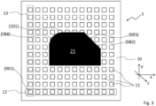
- Fig. 3 illustrates an intensity distribution on the surface of the semiconductor substrate 10 for an exemplary situation where object 2 (not shown in Fig. 3 ) is placed directly on the surface of the magnetic field sensor or the at least partially transparent protection layer.
- object 2 (not shown in Fig. 3 ) is placed directly on the surface of the magnetic field sensor or the at least partially transparent protection layer.
- the presence of the object gives rise to a shaded area 21 in which the intensity is at least essentially equal to zero. Outside said shaded are 21, light from the illumination and/or lighting will reach the surface of the semiconductor substrate 10 at least essentially unobstructed by the object 2, so that intensity in this area will be given by an intensity of the illumination and/or lighting - as transmitted by a partially transparent protection layer if such a layer is present.
- the shaded area 21 is thus indicative of the position and/or orientation of the object relative to the magnetic field sensor array.
- magnetic field sensors numbered 052 to 058, 064 to 070, 078 to 081, and 089 to 092 are completely obstructed and/or shaded off from illumination by object 2. Thus, essentially no light at all from any illumination source will reach said sensors.
- the method in accordance with the second basic embodiment of the invention may, in particular, be carried out in a first variant using a magnetic field sensor array according to one of embodiments 9 to 15 as set forth above, wherein the plurality of light sensitive elements may be used to determine, in particular measure, the first light intensity distribution, from which in turn information on a position and/or orientation of the shadow and/or an area of the magnetic field sensor array obscured by the object may be obtained and/or derived.
- the method may, however, also be carried out using a magnetic field sensor array without any dedicated and/or specific light sensitive elements, in particular with a magnetic field sensor array free of photodetectors, photodiodes and/or CCD cells.
- Temperature sensors may be provided with at least some, in particular all, of the magnetic field sensors.
- a characteristic of Hall sensors is generally temperature dependent, at least a single temperature sensor is provided as part of most magnetic field sensor arrays comprising or made up of Hall sensors.
- Highly accurate Hall sensor arrays generally comprise one temperature sensor for each Hall sensor, wherein each temperature sensor may in particular be arranged closely, in particular as closely as physically possible, to a sensor body and/or the Hall element of each respective Hall sensor.
- the first intensity distribution may thus be determined based on the signals, in particular ordinary signals, delivered by the temperature sensors under adequate illumination conditions, wherein said signals may, in particular, be regarded as intensity signals, possibly containing an at least essentially constant and/or uniform offset.
- An appropriate illumination wavelength or wavelength range or ranges and a sufficient illumination intensity may easily be determined by a person skilled in the art by way of experimentation. In respective experiments, a dependence of ordinary signals provided by the temperature sensors to changing illumination wavelength, wavelength range and/or intensity may be observed, wherein, in particular, any other parameters and/or environmental influence factors may be left unchanged.
- the term "ordinary signal(s)" of a sensor may be understood to refer to such signal(s) and/or measurements as are normally considered indicative of a quantity the sensor is destined to sense and/or measure, and/or analyzed and/or otherwise evaluated to determine and/or obtain such quantity.
- An ordinary signal of a temperature sensor may thus in particular be a temperature signal or measurement.
- the Hall sensors themselves exhibit a light sensitivity which may be sufficiently strong to determine the first intensity distribution with sufficient accuracy from measurements with the magnetic field sensors themselves.
- the first intensity distribution may in particular be determined based on signals, in particular ordinary signals, provided by the plurality of magnetic field sensors under illumination/lightning.
- An ordinary signal of a Hall sensor may accordingly be a magnetic field signal or measurement.
- the signals may, in particular, be regarded as intensity signals, possibly containing an at least essentially constant and/or uniform offset.
- a light sensitivity of a temperature sensor or a Hall sensor may be determined by observing and/or determining how much an ordinary signal, in particular an amplitude thereof, provided by the respective sensors changes when an intensity and/or amplitude of the illumination changes by one or more known amounts or factors.
- the light sensitivity may then be defined as a ratio of the change(s) in signal relative to the change(s) in illumination intensity and/or amplitude.
- Light sensitivities of both temperature sensors and Hall sensor will in general significantly depend on a wavelength or wavelength range or distribution of the illumination, and may accordingly be determined for a plurality of wavelength and/or wavelength ranges.
- Light sensitivity may, in particular, be expressed as a function of wavelength.
- the at least partially transparent protection layer may have a maximum transmittance and/or transmission coefficient at a wavelength or in a wavelength range for which a light sensitivity of the temperature sensors and/or Hall sensors is significantly smaller than a maximum light sensitivity, in particular a maximum of the light sensitivity within the UV-A, visible and/or near-infrared spectral ranges.
- a transmittance and/or transmission coefficient at a wavelength or in a wavelength range for which a light sensitivity of the temperature sensors and/or Hall sensors is at a maximum may be significantly smaller than a maximum transmittance and/or transmission coefficient of the at least partially transparent protection layer. This may, inter alia, reduce a negative impact of ambient light from the UV-A, visible and/or near-infrared spectral ranges on temperature and/or magnetic field measurements.
- An approximate position and/or orientation of the object may rapidly and efficiently be determined by determining for which magnetic field sensors from the magnetic field sensor array illumination is obstructed by the object, and for which ones it is not.
- this determination may be carried out directly on the intensity distribution as determined based on signals, in particular ordinary signals, provided by the plurality of magnetic field sensors.
- signals in particular ordinary signals, provided by the plurality of magnetic field sensors.
- no spatial offset needs to be accounted for, as may, in particular, be the case with the first variant due to the fact that the light sensitive elements need to be provided apart from the magnetic field sensors for elementary reasons.
- An analogous approach may be taken for the second variant, when a distance between magnetic field sensors and respective, associated temperature sensors may be neglected.
- magnetic field sensors 082, 088, 093, and 101 to 104 are partially obstructed and/or shaded off. Under illumination/lighting, said sensors will thus receive some light, albeit with an amount of light reduced as compared to completely unobstructed sensors like, e.g. 001, 0051, 083, 087, etc. It was found that this has the effect that the partially obstructed sensors see an effectively reduced intensity/amplitude as compared to fully unobstructed sensors, wherein a degree and/or amount of reduction is indicative of, in particular corresponds at least approximately to, what percentage of a surface area of a partially obstructed sensor is obstructed by the object.
- Knowledge of which sensors are partially obstructed, in particular together with knowledge of what percentage of a respective surface area of each of said sensors, may be used to enhance an accuracy of the determination of the position and/or orientation of the object.
- a second intensity distribution may be obtained with different illumination conditions present, in particular without illumination.
- a differential intensity distribution may then be obtained by subtracting the first intensity distribution from the second intensity distribution or vice versa.
- the differential intensity distribution may have significantly enhanced contrast, as the difference in illumination level or obscuring the illumination will only affect temperature sensors or magnetic field sensors not fully obstructed by the object. As such, the differential intensity distribution may in particular allow for a more accurate determination of what percentage of the surface area of a partially obstructed sensor is obstructed.
- a respective process may again easily be simplified and/or automized by means of image processing algorithms and/or an image processing system or unit employing such algorithms. These may, in particular be applied to the first intensity distribution as obtained according to the second and third variants as described further above or to the differential intensity distribution, in particular to carry out a number of image corrections and/or enhancements, as for example offset correction, binarization, thresholding, sharpening (in particular of edges), smoothing (in particular of areas), and/or image analysis methods as for example image segregation, object recognition and/or localization, etc.
- image corrections and/or enhancements as for example offset correction, binarization, thresholding, sharpening (in particular of edges), smoothing (in particular of areas), and/or image analysis methods as for example image segregation, object recognition and/or localization, etc.
- Respective data and/or information may again be employed in determining the position and/or orientation, in particular to speed up a determination of the approximate position and/or orientation, and/or enhance an accuracy of said determination.
- information on which sensors would be fully or partially obstructed in particular together with knowledge of what percentage of a respective surface area of each of said sensors, and/or which ones are fully unobstructed, may be derived for each of the hypothetical positions and/or orientations of the object 2.
- An actual position and/or orientation of the shaded area 21, and/or knowledge of which sensors are actually fully or partially obstructed (and to what percentage), and/or which ones are fully unobstructed may then be compared with respective expected data/information for each of the hypothetical positions and/or orientations of the object 2 and a difference and/or deviation be determined and/or measured.
- An actual position and/or orientation of the object may then be assumed to correspond to that hypothetical position and/or orientation of the object for which the difference and/or deviation is smallest as compared to all other hypothetical positions and/or orientations.
- a method in accordance with a third basic embodiment of the invention for determining a magnetic field around an object may comprise the steps of:
- the magnetic field sensor may, in particular, comprise a magnetic field sensitive optical element, in particular layer, configured to generate a photocurrent and/or an electromagnetic radiation, wherein
- the method in accordance with the third basic embodiment of the invention may in particular be applied when using magnetic field sensors and/or cameras as described in or based on the principles described in WO 2022/136175 A1 (cf., in particular, claims 1 and 10), albeit without necessarily making use of all features in any one of the claim, comprised by any one of the embodiments described, and/or of the teachings contained in said document.
- the semiconductor substrate of such magnetic field sensors and/or cameras in itself is, in general, not configured to determine magnetic fields, in particular magnetic flux densities, i.e. without the magnetic field sensitive optical element.
- the semiconductor substrate of such magnetic field sensors and/or cameras may be free of Hall-sensors and/or pick-up coils.
- the magnetic field sensitive optical element may comprise or consist of a first material which, when subjected to a physical excitation and/or physical activation, generates a luminescence or a photocurrent, wherein said luminescence or photocurrent depends on the magnetic flux density.
- the semiconductor substrate may comprise or constitute means for measuring the luminescence, in particular, but not necessarily, by means of a detection signal representing and/or reflecting the strength of the detected luminescence signal or photocurrent signal.
- Physical excitation may be provided electrically or electromagnetically, inter alia optically, in particular by illumination with an appropriate wavelength. Illumination for excitation purposes may also be referred to as excitation illumination and may, in particular, be provided by an excitation light source.
- the first material may comprise or be constituted by a crystalline structure having at least one defect, wherein the first material may, in particular, be diamond, silicon (Si) or SiC, and the defect a colour center - in particular as described in lines 8 to 25 on p. 5 of WO 2022/136175 A1 and the further references cited therein.
- the magnetic field sensitive optical element may, in particular, consist of or comprise a layer of the first material, in particular a diamond layer having nitrogen defects and/or nitrogen-vacancy centers, which exhibits a luminescence which significantly depends on magnetic flux density (cf, WO 2022/136175 A1 , p. 3, first paragraph), in particular decreases with increasing magnetic flux density.
- Excitation may efficiently be provided by excitation illumination with light having wavelengths between 500 and 600nm, while luminescence may occur at wavelengths between 600 and 800nm.
- the semiconductor substrate may, in particular, comprise a photodetector, preferably a plurality of photodetectors, in particular (a) photodiode(s). More specifically, the semiconductor substrate may comprise an image sensor, in particular a CMOS image sensor or a charge-coupled device, CCD, image sensor.
- a photodetector preferably a plurality of photodetectors, in particular (a) photodiode(s).
- the semiconductor substrate may comprise an image sensor, in particular a CMOS image sensor or a charge-coupled device, CCD, image sensor.
- the magnetic field sensitive optical element may be arranged in proximity to the semiconductor substrate, in particular on the semiconductor substrate, and/or the image sensor.
- the optical element is or comprises a layer of the first material
- said layer may preferably be arranged in parallel to a surface of the semiconductor substrate and/or the image sensor, in particular with one or both surfaces of the layer at least essentially parallel to the surface of the semiconductor substrate and/or with the semiconductor substrate located on a first side of the layer.
- the layer and the semiconductor substrate may be arranged in a stacked fashion, and/or in such a way that the layer covers the plurality of photodetectors or the image sensor, preferably the entire image sensor.
- the optical element in particular the layer, may be attached to the semiconductor substrate, in particular in a temporary, releasable and/or separable manner, which may, in particular, allow for the optical element or layer to be separated from the semiconductor substrate without damage to either of them.
- excitation illumination may, in particular, be applied laterally, in particular at and/or through one or more edges of the layer, rather than through one (or both) of the layer's surfaces, in particular by means of LEDs arranged one or more edges.
- Attenuation means for preventing wavelengths other than those of the electromagnetic radiation generated by the magnetic field sensitive optical element, in particular due to luminescence as described above, may be provided between the optical element and the semiconductor substrate, and may, in particular, cover the plurality of photodetectors or the image sensor. Such means may in particular be configured to prevent light having wavelengths used for (optical) excitation of luminescence or photocurrent in the optical element from reaching the photodetectors or the image sensor.
- the plurality of photodetectors or the image sensor may be used to capture an image or a spatial distribution of an intensity of the luminescence, which may be referred to as an activated intensity distribution or luminescence intensity distribution.
- Each signal provided by one of the plurality of the photodetectors or from a pixel of the image sensor may be regarded as a detection signal as mentioned above.
- the image or spatial distribution of the intensity of the luminescence may be considered representative of a spatial distribution of the magnetic field, in particular the magnetic flux density, within the layer of the first material, albeit with in inverse relation, i.e. with regions of relatively low intensities corresponding to regions with relatively strong magnetic field and vice versa.
- a position and/or orientation of the object a magnetic field around which shall be determined may, in particular, be obtained in a manner following the principles as detailed in combination with the second basic embodiment of the invention as detailed above.
- mapping illumination may, in particular, be provided in the form of a collimated beam, that may be directed at least essentially parallel to a surface normal of a surface of the semiconductor substrate, in particular the image sensor, and/or the layer which may constitute the optical element or be comprised by it.
- diffuse lighting and/or illumination may also be used to advantage.
- a light source for providing such illumination in particular a mapping light source, may, in particular, be positioned opposite the semiconductor substrate, with the object located between the light source and the magnetic field sensor array.
- Mapping illumination may in particular employ wavelengths suitable for physical excitation and/or physical activation of the first material, and or corresponding to wavelengths generated by the first material following physical excitation, in particular when attenuation means as described above are present in the magnetic field sensor.
- Fig. 4 illustrates an exemplary first intensity distribution on the surface of the semiconductor substrate 10' for an exemplary situation where object 2 (not shown in Fig. 4 ) is placed above, adjacent to and/or opposite the semiconductor substrate and/or the magnetic field sensitive optical element (not shown in Fig. 4 ).
- a plurality of pixels 31 is formed in the semiconductor substrate and arranged in lines and columns.
- index s 12 ( n -1) + m .
- a shaded area 21' in which a first or obstructed intensity is at least essentially equal to zero.
- light from the illumination and/or lighting will reach the surface of the semiconductor substrate 10 at least essentially unobstructed by the object 2, so that a second or unobstructed intensity in this area will be given by an intensity of the illumination and/or lighting - as possibly attenuated by the attenuation means or other means if present.
- the shaded area 21' is thus indicative of the position and/or orientation of the object relative to the magnetic field sensor array.
- the second or unobstructed intensity may at least partially be contributed to by luminescence, which may occur outside shaded area 21' when mapping illumination contains wavelengths capable of exciting electromagnetic radiation from the magnetic field sensitive optical element. Within shaded area 21', on the other hand, no luminescence is received in general.
- An approximate position and/or orientation of the object may rapidly and efficiently be deter-mined by determining for which of the plurality of photodetectors or for which pixels of the image sensor illumination is obstructed by the object, and for which ones it is not.
- pixels numbered 052 to 058, 064 to 070, 078 to 081, and 089 to 092 are completely obstructed and/or shaded off from illumination by object 2. Thus, essentially no light at all from any illumination source will reach said sensors.
- pixels 082, 088, 093, and 101 to 104 are partially obstructed and/or shaded off. Under illumination/lighting, said pixels will thus receive some light, albeit with an amount of light reduced as compared to completely unobstructed sensors like, e.g. 001, 0051, 083, 087, etc. It was found that this has the effect that the partially obstructed pixels see an effectively reduced intensity/amplitude as compared to fully unobstructed pixels, wherein a degree and/or amount of reduction is indicative of, in particular corresponds at least approximately to, what percentage of a surface area of a partially obstructed pixels is obstructed by the object 2.
- Knowledge of which pixels are partially obstructed, in particular together with knowledge of what percentage of a respective surface area of each of said pixels, may be used to enhance an accuracy of the determination of the position and/or orientation of the object.
- a second intensity distribution may be obtained with different illumination conditions present, in particular without illumination.
- a differential intensity distribution may then be obtained by subtracting the first intensity distribution from the second intensity distribution or vice versa.
- the differential intensity distribution may have significantly enhanced contrast, as the difference in illumination level or obscuring the illumination will only affect pixels not fully obstructed by the object.
- the differential intensity distribution may in particular allow for a more accurate determination of what percentage of the surface area of a partially obstructed sensor is obstructed.
- a respective process may again easily be simplified and/or automized by means of image processing algorithms and/or an image processing system or unit employing such algorithms. These may, in particular be applied to the first intensity distribution, in particular to carry out a number of image corrections and/or enhancements, as for example offset correction, binarization, thresholding, sharpening (in particular of edges), smoothing (in particular of areas), and/or image analysis methods as for example image segregation, object recognition and/or localization, etc.
- image corrections and/or enhancements as for example offset correction, binarization, thresholding, sharpening (in particular of edges), smoothing (in particular of areas), and/or image analysis methods as for example image segregation, object recognition and/or localization, etc.
- Respective data and/or information may again be employed in determining the position and/or orientation, in particular to speed up a determination of the approximate position and/or orientation, and/or enhance an accuracy of said determination.
- simulations may be carried out, in particular on a computer which may employ ray-tracing methods, algorithms and/or software to determine, from the data and or information on the known geometry and/or dimensions of the object, and, in particular, information, in particular parameters, regarding the illumination and/or the light source, an expected position and/or orientation of the shaded area 21 for a plurality of hypothetical positions and/or orientations of the object 2.
- information on which sensors would be fully or partially obstructed in particular together with knowledge of what percentage of a respective surface area of each of said sensors, and/or which ones are fully unobstructed, may be derived for each of the hypothetical positions and/or orientations of the object 2.
- An actual position and/or orientation of the shaded area 21, and/or knowledge of which sensors are actually fully or partially obstructed (and to what percentage), and/or which ones are fully unobstructed, may then be compared with respective expected data/information for each of the hypothetical positions and/or orientations of the object 2 and a difference and/or deviation be determined and/or measured.
- An actual position and/or orientation of the object may then be assumed to correspond to that hypothetical position and/or orientation of the object for which the difference and/or deviation is smallest as compared to all other hypothetical positions and/or orientations.
- the magnetic field sensor and/or camera may, in addition to the semiconductor substrate and the magnetic field sensitive optical element, comprise means for physical excitation integrally formed with the magnetic field sensitive optical element.
- the optical element is or comprises a (first) layer of the first material
- such means may be provided on a second side of said layer, in particular opposite and/or across from the semiconductor substrate, and/or with said second side facing away from the semiconductor substrate, and may also consist of or comprise a (second) layer.
- Such means for means for physical excitation may, in particular, comprise an LED structure as described on p. 14 of WO 2022/136175 A1 .
- the object a magnetic field around which shall be determined may then be placed adjacent to the means for physical excitation, in particular onto or on said means.
- Means for physical excitation as described in the preceding paragraph may complicate mapping illumination, as they may substantially obstruct and/or absorb light emitted from the mapping light source, and thus reduce the effective sensitivity of the plurality of photodetectors or the pixels of the image sensor to mapping illumination. This may, e.g., be overcome by obtaining a differential intensity distribution as described further above.
- the present disclosure also includes embodiments with any combination of features which are mentioned or shown above and/or below, in various embodiments or variants. It also includes individual features as shown in the Figures, even if they are shown there in connection with other features and/or are not mentioned above or below.
- the disclosure comprises embodiments which exclusively comprise the features described in the claims or the exemplary embodiments, as well as those which comprise additional other features.
- the steps of any method disclosed above or claimed below may preferably be carried out according to the order in which they are presented, but may also be carried out in a different order.
- a ⁇ b may imply that
- ) ⁇ 0.01, wherein a and b may represent arbitrary quantities, parameters and/or variables as described and/or defined anywhere in this document, or as otherwise known to a person skilled in the art. Further, a statement that a is at least approximately equal or at least approximately identical to b may imply that a ⁇ b, and not exclude that a b.
- a statement a ⁇ b may imply that a > 5 b , preferably a > 100 b ; and statement a ⁇ b may imply that 5 a ⁇ b, preferably 100 a ⁇ b.
- a statement that a is significantly larger than b may imply that a ⁇ b.
- a statement that a is significantly smaller than b may imply that a ⁇ b.
- connection in particular between any two entities, including in particular nodes, points, terminals, elements, devices, etc. or combinations thereof, may refer to an electrically conductive connection, as in particular established by a wire, cable, busbar, a conductive track, trace or line on e.g. a (printed) circuit board, solder, etc.
- the electrically conductive connection is preferably at least substantially direct, in particular without any discrete elements, as, in particular, resistors, capacitors, inductors, or other passive or active elements or devices connected between the connected entities.
- the electrically conductive connection thus has at least essentially negligible resistance, capacitance and inductance, preferably at least essentially zero resistance, capacitance and inductance.
- resistance, capacitance and inductance of the electrically conductive connection are exclusively parasitic by nature.
- resistance, capacitance and inductance of the electrically conductive connection significantly smaller (preferably by a factor of 1/100, 1/1000 or 1/10000) than resistances, capacitances and impedances of resistors, capacitors or inductors, respectively, connected by the electrical conductive connection, and/or comprised by an electric circuit or network which comprises the electrically conductive connection.
- any one of an electric connection, electrical connection, conductive connection, conducting connection may be identical to a connection as defined above.
- connection as defined above may exist between the two entities.
Landscapes
- Physics & Mathematics (AREA)
- Condensed Matter Physics & Semiconductors (AREA)
- General Physics & Mathematics (AREA)
- Measuring Magnetic Variables (AREA)
Priority Applications (3)
| Application Number | Priority Date | Filing Date | Title |
|---|---|---|---|
| CN202480039030.5A CN121336119A (zh) | 2023-06-12 | 2024-04-09 | 磁场传感器阵列和用于测量磁场的方法等 |
| PCT/EP2024/059639 WO2024256060A1 (en) | 2023-06-12 | 2024-04-09 | Magnetic field sensor array and method for measuring a magnetic field, etc. |
| EP24723011.3A EP4724827A1 (de) | 2023-06-12 | 2024-04-09 | Magnetfeldsensoranordnung und verfahren zur messung eines magnetfeldes etc |
Applications Claiming Priority (3)
| Application Number | Priority Date | Filing Date | Title |
|---|---|---|---|
| CH8292023 | 2023-07-31 | ||
| CH8452023 | 2023-08-05 | ||
| EP23020566 | 2023-12-20 |
Publications (1)
| Publication Number | Publication Date |
|---|---|
| EP4502635A1 true EP4502635A1 (de) | 2025-02-05 |
Family
ID=90362451
Family Applications (1)
| Application Number | Title | Priority Date | Filing Date |
|---|---|---|---|
| EP24020077.4A Pending EP4502635A1 (de) | 2023-06-12 | 2024-03-11 | Magnetfeldsensoranordnung und verfahren zur messung eines magnetfeldes etc |
Country Status (1)
| Country | Link |
|---|---|
| EP (1) | EP4502635A1 (de) |
Citations (5)
| Publication number | Priority date | Publication date | Assignee | Title |
|---|---|---|---|---|
| JP2009086183A (ja) * | 2007-09-28 | 2009-04-23 | Casio Comput Co Ltd | 磁気検知型入力パネル及び入力パネル付き表示装置 |
| US20160313408A1 (en) * | 2015-04-21 | 2016-10-27 | Renesas Electronics Corporation | Magnetic measuring device |
| US20210041513A1 (en) * | 2019-08-06 | 2021-02-11 | Hi Llc | Systems and methods having an optical magnetometer array with beam splitters |
| WO2022136275A1 (en) | 2020-12-22 | 2022-06-30 | Fluigent | Apparatus for controlling pressure or flow in a fluidic system |
| WO2022136175A1 (de) | 2020-12-23 | 2022-06-30 | Quantum Technologies UG | Verfahren und vorrichtung zur bestimmung einer magnetischen flussdichte sowie verfahren zur herstellung einer solchen vorrichtung |
-
2024
- 2024-03-11 EP EP24020077.4A patent/EP4502635A1/de active Pending
Patent Citations (5)
| Publication number | Priority date | Publication date | Assignee | Title |
|---|---|---|---|---|
| JP2009086183A (ja) * | 2007-09-28 | 2009-04-23 | Casio Comput Co Ltd | 磁気検知型入力パネル及び入力パネル付き表示装置 |
| US20160313408A1 (en) * | 2015-04-21 | 2016-10-27 | Renesas Electronics Corporation | Magnetic measuring device |
| US20210041513A1 (en) * | 2019-08-06 | 2021-02-11 | Hi Llc | Systems and methods having an optical magnetometer array with beam splitters |
| WO2022136275A1 (en) | 2020-12-22 | 2022-06-30 | Fluigent | Apparatus for controlling pressure or flow in a fluidic system |
| WO2022136175A1 (de) | 2020-12-23 | 2022-06-30 | Quantum Technologies UG | Verfahren und vorrichtung zur bestimmung einer magnetischen flussdichte sowie verfahren zur herstellung einer solchen vorrichtung |
Non-Patent Citations (1)
| Title |
|---|
| HALL EFFECT SENSOR, 3 April 2023 (2023-04-03), Retrieved from the Internet <URL:https://de.wikipedia.orq/w/index.php?title=HaII-Sensor&oldid=232440088> |
Similar Documents
| Publication | Publication Date | Title |
|---|---|---|
| US11536815B2 (en) | Optoelectronic modules operable to recognize spurious reflections and to compensate for errors caused by spurious reflections | |
| KR101692115B1 (ko) | 검사 장치 및 검사 방법 | |
| CN109642950A (zh) | 用于飞行时间测量的光学传感器模块和用于制造光学传感器模块的方法 | |
| TWI445929B (zh) | A light emission measuring device, a light emission measuring method, a control program, and a readable recording medium | |
| US20110175987A1 (en) | Stereo camera system | |
| CN106462765A (zh) | 具有像素内光学传感器的指纹传感器 | |
| KR20160045670A (ko) | 비행-시간 카메라 시스템 | |
| US9354045B1 (en) | Image based angle sensor | |
| CN1293361C (zh) | 测量系统中的装置 | |
| CN112469977A (zh) | 多光谱传感器和用于多光谱光感测的方法 | |
| CN102261895A (zh) | 区别对象区与基底区的方法及用该方法测量三维形状的方法 | |
| CN114397694A (zh) | 一种x射线双能谱探测线阵探测器 | |
| US9729738B2 (en) | Image reading device | |
| CN104515477A (zh) | 三维测定装置、三维测定方法以及基板的制造方法 | |
| EP3091363B1 (de) | Magnetoresistives bildsensorarray mit niedrigem profil | |
| US9883168B2 (en) | Camera module having an array sensor | |
| KR102842618B1 (ko) | 통합 자력계 및 자기장을 검출하는 방법 | |
| KR102234984B1 (ko) | 반도체 웨이퍼의 파티클 검출장치 | |
| EP4724827A1 (de) | Magnetfeldsensoranordnung und verfahren zur messung eines magnetfeldes etc | |
| US10429239B2 (en) | Color capture arrangement and correction method using the color capture arrangement | |
| CN203759230U (zh) | 一种磁电阻成像传感器阵列 | |
| JP6155452B1 (ja) | 基板上の粒子の検出装置 | |
| US9774771B2 (en) | Preparation, transparent plate, method for producing preparation, slide glass, imaging apparatus, imaging method, preparation producing apparatus, and preparation component set | |
| US12603472B2 (en) | Time-of-flight sensor and manufacturing method thereof | |
| CN104157071A (zh) | 磁图像防伪系统及方法 |
Legal Events
| Date | Code | Title | Description |
|---|---|---|---|
| PUAI | Public reference made under article 153(3) epc to a published international application that has entered the european phase |
Free format text: ORIGINAL CODE: 0009012 |
|
| STAA | Information on the status of an ep patent application or granted ep patent |
Free format text: STATUS: THE APPLICATION HAS BEEN PUBLISHED |
|
| AK | Designated contracting states |
Kind code of ref document: A1 Designated state(s): AL AT BE BG CH CY CZ DE DK EE ES FI FR GB GR HR HU IE IS IT LI LT LU LV MC ME MK MT NL NO PL PT RO RS SE SI SK SM TR |
|
| STAA | Information on the status of an ep patent application or granted ep patent |
Free format text: STATUS: REQUEST FOR EXAMINATION WAS MADE |
|
| 17P | Request for examination filed |
Effective date: 20250802 |