EP4502809A1 - Datenschreibverfahren und verarbeitungssystem - Google Patents
Datenschreibverfahren und verarbeitungssystem Download PDFInfo
- Publication number
- EP4502809A1 EP4502809A1 EP23791247.2A EP23791247A EP4502809A1 EP 4502809 A1 EP4502809 A1 EP 4502809A1 EP 23791247 A EP23791247 A EP 23791247A EP 4502809 A1 EP4502809 A1 EP 4502809A1
- Authority
- EP
- European Patent Office
- Prior art keywords
- data
- memory
- memory space
- symbols
- redundant
- Prior art date
- Legal status (The legal status is an assumption and is not a legal conclusion. Google has not performed a legal analysis and makes no representation as to the accuracy of the status listed.)
- Pending
Links
Images






Classifications
-
- G—PHYSICS
- G06—COMPUTING OR CALCULATING; COUNTING
- G06F—ELECTRIC DIGITAL DATA PROCESSING
- G06F11/00—Error detection; Error correction; Monitoring
- G06F11/07—Responding to the occurrence of a fault, e.g. fault tolerance
- G06F11/08—Error detection or correction by redundancy in data representation, e.g. by using checking codes
- G06F11/10—Adding special bits or symbols to the coded information, e.g. parity check, casting out 9's or 11's
- G06F11/1008—Adding special bits or symbols to the coded information, e.g. parity check, casting out 9's or 11's in individual solid state devices
- G06F11/1044—Adding special bits or symbols to the coded information, e.g. parity check, casting out 9's or 11's in individual solid state devices with specific ECC/EDC distribution
-
- G—PHYSICS
- G06—COMPUTING OR CALCULATING; COUNTING
- G06F—ELECTRIC DIGITAL DATA PROCESSING
- G06F12/00—Accessing, addressing or allocating within memory systems or architectures
- G06F12/02—Addressing or allocation; Relocation
- G06F12/0223—User address space allocation, e.g. contiguous or non contiguous base addressing
- G06F12/0284—Multiple user address space allocation, e.g. using different base addresses
-
- G—PHYSICS
- G06—COMPUTING OR CALCULATING; COUNTING
- G06F—ELECTRIC DIGITAL DATA PROCESSING
- G06F11/00—Error detection; Error correction; Monitoring
- G06F11/07—Responding to the occurrence of a fault, e.g. fault tolerance
- G06F11/08—Error detection or correction by redundancy in data representation, e.g. by using checking codes
- G06F11/10—Adding special bits or symbols to the coded information, e.g. parity check, casting out 9's or 11's
- G06F11/1008—Adding special bits or symbols to the coded information, e.g. parity check, casting out 9's or 11's in individual solid state devices
- G06F11/1068—Adding special bits or symbols to the coded information, e.g. parity check, casting out 9's or 11's in individual solid state devices in sector programmable memories, e.g. flash disk
-
- G—PHYSICS
- G06—COMPUTING OR CALCULATING; COUNTING
- G06F—ELECTRIC DIGITAL DATA PROCESSING
- G06F11/00—Error detection; Error correction; Monitoring
- G06F11/07—Responding to the occurrence of a fault, e.g. fault tolerance
- G06F11/08—Error detection or correction by redundancy in data representation, e.g. by using checking codes
- G06F11/10—Adding special bits or symbols to the coded information, e.g. parity check, casting out 9's or 11's
- G06F11/1008—Adding special bits or symbols to the coded information, e.g. parity check, casting out 9's or 11's in individual solid state devices
- G06F11/1048—Adding special bits or symbols to the coded information, e.g. parity check, casting out 9's or 11's in individual solid state devices using arrangements adapted for a specific error detection or correction feature
-
- G—PHYSICS
- G06—COMPUTING OR CALCULATING; COUNTING
- G06F—ELECTRIC DIGITAL DATA PROCESSING
- G06F12/00—Accessing, addressing or allocating within memory systems or architectures
- G06F12/02—Addressing or allocation; Relocation
- G06F12/0223—User address space allocation, e.g. contiguous or non contiguous base addressing
-
- G—PHYSICS
- G06—COMPUTING OR CALCULATING; COUNTING
- G06F—ELECTRIC DIGITAL DATA PROCESSING
- G06F3/00—Input arrangements for transferring data to be processed into a form capable of being handled by the computer; Output arrangements for transferring data from processing unit to output unit, e.g. interface arrangements
- G06F3/06—Digital input from, or digital output to, record carriers, e.g. RAID, emulated record carriers or networked record carriers
- G06F3/0601—Interfaces specially adapted for storage systems
- G06F3/0602—Interfaces specially adapted for storage systems specifically adapted to achieve a particular effect
- G06F3/061—Improving I/O performance
-
- G—PHYSICS
- G06—COMPUTING OR CALCULATING; COUNTING
- G06F—ELECTRIC DIGITAL DATA PROCESSING
- G06F3/00—Input arrangements for transferring data to be processed into a form capable of being handled by the computer; Output arrangements for transferring data from processing unit to output unit, e.g. interface arrangements
- G06F3/06—Digital input from, or digital output to, record carriers, e.g. RAID, emulated record carriers or networked record carriers
- G06F3/0601—Interfaces specially adapted for storage systems
- G06F3/0628—Interfaces specially adapted for storage systems making use of a particular technique
- G06F3/0629—Configuration or reconfiguration of storage systems
-
- G—PHYSICS
- G06—COMPUTING OR CALCULATING; COUNTING
- G06F—ELECTRIC DIGITAL DATA PROCESSING
- G06F2212/00—Indexing scheme relating to accessing, addressing or allocation within memory systems or architectures
- G06F2212/10—Providing a specific technical effect
- G06F2212/1032—Reliability improvement, data loss prevention, degraded operation etc
Definitions
- This application relates to the field of computer technologies, and in particular, to a data writing method and a processing system.
- This application provides a data writing method and a processing system, to improve an error detection capability and an error correction capability of a processing system, and improve system reliability.
- a first aspect of this application provides a data writing method, where the method is applied to a processing system, the processing system includes a first memory, and the first memory includes a plurality of memory spaces; and the method includes: obtaining first data, where the first data is data to be written into the first memory; determining, based on first error distribution area information of at least one memory space in the plurality of memory spaces, a first arrangement manner of a memory space occupied by a data symbol; determining the first data as M data symbols based on the first arrangement manner of the memory space occupied by the data symbol, where each of the M data symbols includes a plurality of data bits, and M is an integer greater than or equal to 1; performing first ECC encoding on the M data symbols to obtain N first redundant symbols, where each of the N first redundant symbols includes at least one redundant bit, and N is an integer greater than or equal to 1; and writing the M data symbols into a data memory space of the first memory, and writing the N first redundant symbols into a first ECC memory space of the first memory.
- the processing system determines, based on the first error distribution area information of the at least one memory space in the plurality of memory spaces, the first arrangement manner of the memory space occupied by the data symbol.
- the processing system designs, with reference to distribution of error areas in the at least one memory space, an arrangement manner of the memory space occupied by the data symbol.
- the processing system determines the first data as the M data symbols with reference to the first arrangement manner of the memory space occupied by the data symbol, where each of the M data symbols includes the data bits.
- the processing system divides, with reference to the first arrangement manner, the data bits that are in the first data and that can form a shape of the first arrangement manner into a same data symbol. Therefore, this helps perform maximized error detection and maximized error correction on data in a subsequent data reading process of the processing system.
- An error detection capability and an error correction capability of the processing system are improved, and system reliability is improved. In this way, a maximized error detection capability and a maximized error correction capability of the first ECC memory space of the first memory are fully utilized, a data error area is covered to a maximum extent, and the system reliability is improved.
- the first error distribution area information of the at least one memory space indicates a specific area, in the at least one memory space, in which an error data bit falls when a data error occurs in the at least one memory space.
- the first error distribution area information indicates an area range in which the error data bit usually falls when the data error occurs in the at least one memory space.
- the area range is less than a size of the at least one memory space. Therefore, the processing system can determine, with reference to the area range, an arrangement manner of the memory space occupied by the data symbol. Then, the processing system divides, with reference to the first arrangement manner, the data bits that are in the first data and that can form the shape of the first arrangement manner into a same data symbol. Therefore, this helps perform maximized error detection and maximized error correction on the data in the subsequent data reading process of the processing system.
- the error detection capability and the error correction capability of the processing system are improved, and the system reliability is improved. In this way, the maximized error detection capability and the maximized error correction capability of the first ECC memory space of the first memory are fully utilized, the data error area is covered to the maximum extent, and the system reliability is improved.
- each data symbol occupies an 8-bit memory space
- the first arrangement manner of the memory space occupied by the data symbol includes any one of the following: arrangement in four rows and two columns, arrangement in two rows and four columns, arrangement in eight rows and one column, and arrangement in one row and eight columns; or
- the method further includes: obtaining the first error distribution area information of the at least one memory space in the plurality of memory spaces.
- the processing system may obtain the first error distribution area information, so that the processing system determines the first arrangement manner of the memory space occupied by the data symbol.
- the processing system may obtain the first error distribution area information through an external interface.
- the processing system obtains the first error distribution area information by using preconfigured information.
- the method further includes: reading all data from the first memory, where all the data includes data bits and a redundant bit; determining, based on second error distribution area information of the at least one memory space in the plurality of memory spaces, a second arrangement manner of the memory space occupied by the data symbol; determining the data bits in all the data as P data symbols based on the second arrangement manner of the memory space occupied by the data symbol, where each of the P data symbols includes a plurality of data bits, and P is an integer greater than or equal to 1; performing first ECC encoding on the P data symbols to obtain Q first redundant symbols, where each of the Q first redundant symbols includes at least one redundant bit, and Q is an integer greater than or equal to 1; and writing the P data symbols into the data memory space of the first memory, and writing the Q first redundant symbols into the first ECC memory space of the first memory.
- the processing system may read all the data from the first memory, and then determine, with reference to the second error distribution area information, the second arrangement manner of the memory space occupied by the data symbol. Then, the processing system performs encoding based on the second arrangement manner and the data bits in all the data. Therefore, an arrangement manner of the memory space occupied by the data symbol is changed, and the processing system can perform maximized error detection and maximized error correction on the data in the subsequent data reading process. The error detection capability and the error correction capability of the processing system are improved.
- the method further includes: obtaining the second error distribution area information of the at least one memory space in the plurality of memory spaces.
- the processing system obtains the second error distribution area information, so that the processing system re-encodes and writes the data, to change an arrangement manner of a content space occupied by the data symbol, and the processing system can perform maximized error detection and maximized error correction on the data in the subsequent data reading process.
- the obtaining the second error distribution area information of the at least one memory space in the plurality of memory spaces includes: determining the second error distribution area information of the at least one memory space in the plurality of memory spaces based on a historical data error.
- the processing system may determine the second error distribution area information with reference to the historical data error. In other words, the processing system may dynamically change an error distribution area of the at least one memory space with reference to an actual situation. Therefore, the solution is more applicable to an actual application scenario, and practicability of the solution is improved.
- the data symbol and the first redundant symbol are Reed-Solomon (reed-solomon code, RS) code symbols; or the data symbol and the first redundant symbol are Bose-Chaudhuri-Hocquenghem (Bose Ray-Chaudhuri Hocquenghem, BCH) code symbols.
- RS Reed-Solomon code
- BCH Bose Ray-Chaudhuri Hocquenghem
- some possible forms of the data symbol and the first redundant symbol are provided, and are specifically determined based on an encoding algorithm used for the processing system, to facilitate implementation of the solution.
- the performing first ECC encoding on the M data symbols to obtain N first redundant symbols includes: performing first ECC encoding on the M data symbols by using a finite field encoding algorithm to obtain the N first redundant symbols, where the finite field encoding algorithm includes an RS algorithm, a BCH algorithm, or the like.
- the processing system may perform ECC encoding on the M data symbols by using the finite field encoding algorithm, to implement ECC protection on the data. This facilitates the processing system to perform maximized error correction and maximized error detection on the data subsequently. The error detection capability and the error correction capability of the processing system are improved.
- the first memory is a memory that supports second ECC encoding, and the first memory further includes a second ECC memory space; and the method includes:
- the first memory further includes the second ECC memory space
- the processing system may further perform second ECC encoding on the M data symbols and the N first redundant symbols. Therefore, further second-level ECC protection is implemented for the M data symbols and the N first redundant symbols.
- the first memory is an on die error correction code (on die ECC) memory.
- on die ECC on die error correction code
- the first memory may be the on die ECC memory.
- a data bit read by the processing system may be obtained through error detection and error correction processing performed by the on die ECC memory.
- the first ECC memory space and an on die ECC memory space of the first memory can jointly perform error detection and error correction on the data. The error detection capability and the error correction capability of the processing system are improved, and the system reliability is improved.
- a second aspect of this application provides a processing system.
- the processing system includes a first memory, the first memory includes a plurality of memory spaces, and the processing system includes:
- the first error distribution area information of the at least one memory space indicates a specific area, in the at least one memory space, in which an error data bit falls when a data error occurs in the at least one memory space.
- each data symbol occupies an 8-bit memory space
- the first arrangement manner of the memory space occupied by the data symbol includes any one of the following: arrangement in four rows and two columns, arrangement in two rows and four columns, arrangement in eight rows and one column, and arrangement in one row and eight columns; or
- the obtaining unit is further configured to: obtain the first error distribution area information of the at least one memory space in the plurality of memory spaces.
- the processing system further includes a reading unit.
- the reading unit is configured to read all data from the first memory, where all the data includes data bits and a redundant bit.
- first ECC encoding may also be referred to as first-level ECC encoding.
- FIG. 7a to FIG. 7d are described by using an example in which a size of an error detection space and a size of an error correction space in the first ECC memory space of the first memory are 1:1. In other words, a ratio of an error correction symbol to an error detection symbol is 1:1.
- An arrangement manner of a memory space occupied by the error detection symbol may be the first arrangement manner. The error detection symbol is not described in detail in the following.
- the encoding codeword length in the second ECC memory space of each memory device may include 512 data bits and 32 redundant bits. This is not specifically limited in this application.
- the second ECC encoding may also be referred to as second-level ECC encoding.
- the first memory controller 201 writes the M data symbols into the data memory space of the first memory, and writes the N first redundant symbols into the first ECC memory space of the first memory.
- the processing system writes data bits included in the M data symbols into the data memory space of the first memory, and writes redundant bits included in the N first redundant symbols into the first ECC memory space of the first memory.
- a specific arrangement manner of a memory space occupied by the data symbol or the first redundant symbol is shown in FIG. 9 .
- the arrangement manner of the memory space occupied by the data symbol or the first redundant symbol is the arrangement in the 16 rows and the one column.
- the embodiment shown in FIG. 3 further includes step 305a.
- Step 305a may be performed before step 305.
- the second ECC encoding may include: The processing system performs Hamming code encoding on the M data symbols and the N first redundant symbols as the data to obtain the R second redundant symbols.
- the first memory controller 201 performs first ECC encoding on the M data symbols to obtain N first redundant symbols. Then, the first memory controller 201 performs second ECC encoding on the M data symbols and the N first redundant symbols as the data to obtain the R second redundant symbols.
- the first memory controller 203 performs first ECC encoding on the M data symbols to obtain N first redundant symbols. Then, the first memory controller 203 transmits the M data symbols and the N first redundant symbols to the second memory controller 204 through a memory interface. The second memory controller 204 performs second ECC encoding on the M data symbols and the N first redundant symbols as the data to obtain the R second redundant symbols.
- step 305 specifically includes: writing the M data symbols into the data memory space of the first memory, writing the N first redundant symbols into the first ECC memory space of the first memory, and writing the R second redundant symbols into the second ECC memory space of the first memory.
- the second memory controller 204 performs second ECC encoding on the data symbol 1 to a data symbol 8 that are to be stored into the data device 1, to obtain a second redundant symbol of the data device 1. Then, the second memory controller 204 separately writes the data symbol 1 to the data symbol 8 and the second redundant symbol of the data device 1 into spatial locations corresponding to the data device 1. The second memory controller 204 performs second ECC encoding on a data symbol 9 to a data symbol 16 that are to be stored into a data device 2, to obtain a second redundant symbol of the data device 2. Then, the second memory controller 204 writes the data symbol 9 to the data symbol 16 and the second redundant symbol of the data device 2 into the data device 2.
- Scenario 1 In a process in which the processing system reads the M data symbols and the N first redundant symbols from the first memory, if the second memory controller 204 performs read error detection and detects no error, the second memory controller 204 discards the second redundant symbol. Then, the second memory controller 204 transmits the M data symbols and the N first redundant symbols back to the first memory controller 203 through a first memory channel.
- Scenario 2 In a process in which the processing system reads the M data symbols and the N first redundant symbols from the first memory, if the second memory controller 204 performs read error detection and detects an error, and a range of error data is within an error correction capability range of the second memory controller 204, the second memory controller 204 performs error correction by using the second redundant symbol. Then, the second memory controller 204 transmits corrected M data symbols and N first redundant symbols back to a buffer of the first memory controller 203 through a first memory channel.
- Scenario 3 In a process in which the processing system reads the M data symbols and the N first redundant symbols from the first memory, if the second memory controller 204 performs read error detection and detects an error, and a range of error data exceeds an error correction capability range of the second memory controller 204, the second memory controller 204 discards the second redundant symbol (in other words, does not perform second ECC error correction).
- the second memory controller 204 directly transmits the M data symbols and the N first redundant symbols back to the first memory controller 203 through a first memory channel.
- the second memory controller 204 sends an error notification to the first memory controller 203, to indicate that the second memory controller 204 detects the error in the M data symbols but fails to correct the error.
- Scenario 4 In a process in which the processing system reads the M data symbols and the N first redundant symbols from the first memory, if the second memory controller 204 performs read error detection and detects an error, and a range of error data exceeds an error detection capability range of the second memory controller 204, the second memory controller 204 may mistakenly consider that error correction can be performed and attempt to perform error correction, and may miscorrect the data. In other words, an error area is further expanded. However, the second memory controller does not know. Then, the second memory controller 204 transmits, back to the first memory controller 203 through a first memory channel, M data symbols and N first redundant symbols that are obtained through second ECC correction.
- This scenario is a second ECC (for example, the on die ECC) miscorrection scenario.
- the technical solutions of this application are applicable to the foregoing scenario 1 to scenario 4, especially the miscorrection scenario in the scenario 4.
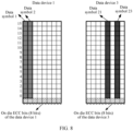
- the scenario 2 and the scenario 4 when the second memory controller 204 performs error correction on the M data symbols and the N first redundant symbols by using the R second redundant symbols, a specially designed generator matrix of second ECC code is used, and a result is that a data change range in a second ECC error correction process is limited to a small range, for example, a leftmost 1/4 memory space of a memory space occupied by "the M data symbols and the N first redundant symbols". Therefore, the first error distribution area information indicates information such as the error area detected in the second ECC memory space or the additional miscorrection area generated by performing error correction in the second ECC memory space.
- the processing system may set, in a data writing process, an appropriate arrangement manner of a memory space occupied by a symbol, so that the processing system performs maximized error detection and maximized error correction on data in the miscorrection scenario in the scenario 4 subsequently.
- the processing system may read the M data symbols and the N first redundant symbols from the first memory. If the first memory is the memory that supports the second ECC encoding (for example, the on die ECC), both the M data symbols and the N first redundant symbols may be obtained by performing error detection and error correction processing in the second ECC memory space. Specifically, as shown in FIG. 9 , the M data symbols include the data symbol 1 to the data symbol 32. The N first redundant symbols include a first redundant symbol 1 to the second redundant symbol (which may also be referred to as an error correction symbol 1 to an error correction symbol 4) and an error detection symbol in the error detection space. The error detection space includes four error detection symbols. Therefore, the processing system can detect a maximum of four error data symbols.
- the M data symbols include the data symbol 1 to the data symbol 32.
- the N first redundant symbols include a first redundant symbol 1 to the second redundant symbol (which may also be referred to as an error correction symbol 1 to an error correction symbol 4) and an error detection symbol in the error detection space.
- the error detection space includes four error
- the processing system performs error detection on a data symbol in a third data by using the error detection symbol in the error detection space, to determine that errors occur in data bits in the data symbol 1, the data symbol 2, a data symbol 21, and the data symbol 23. Specifically, the processing system may determine how many data bit errors may exist in the data symbol 1, the data symbol 2, the data symbol 21, and the data symbol 23. Because one error correction symbol can correct one data symbol, the processing system may use the first redundant symbol 1 to correct the data symbol 1, use a first redundant symbol 2 to correct the data symbol 2, use a first redundant symbol 3 to correct the data symbol 21, and use the first redundant symbol 4 to correct the data symbol 23. It should be noted that any error correction symbol can correct any data symbol. For example, the processing system herein may alternatively use the first redundant symbol 2 to correct the data symbol 1. This is not specifically limited in this application.
- the first memory controller may be notified of an error detection result and an error correction status of the second ECC memory space by using Alert_N Pin. Therefore, the first memory controller may determine the error detection result and the error correction status of the second ECC memory space. This helps further enhance an error detection capability and an error correction capability of the first memory controller.
- the processing system determines, with reference to the first error distribution area information of the at least one memory space in the plurality of memory spaces, the first arrangement manner of the memory space occupied by the data symbol.
- the first arrangement manner matches or is strongly associated with the arrangement manner of the specific area indicated by the first error distribution area information.
- the first memory may be a memory storage medium that supports second-level ECC, and M data bits may be obtained by performing error detection and error correction in the second ECC memory space.
- first-level ECC memory and the second-level ECC can jointly perform error detection and error correction on the data, so that the system reliability is improved.
- the first memory may be the memory that supports the second ECC encoding (for example, the on die ECC), and the M data bits may be obtained by performing error detection and error correction processing in the second ECC memory space.
- the first-level ECC memory and the second-level ECC jointly perform error detection and error correction on the data, to implement first-layer ECC protection and second-layer ECC protection for the data, and implement collaboration to achieve more powerful error detection, error correction, and fault tolerance capabilities.
- the technical solutions of this application are described herein by using two-layer ECC protection as an example.
- the processing system can provide ECC protection for data at more layers.
- the processing system may further implement third-layer ECC protection on the data by using another ECC memory. This is not specifically limited in this application.
- the processing system can detect only four data symbol errors by using the error detection symbols in the error detection space. For example, the processing system detects that errors occur in a data symbol 1 to a data symbol 4, and cannot detect that errors also occur in a data symbol 21 to a data symbol 24. In other words, eight data symbol errors actually occur, but the processing system can detect only four data symbol errors. Specifically, the processing system may determine how many data bit errors exist in each data symbol of the data symbol 1 to the data symbol 4.
- the processing system may use a first redundant symbol 1 to correct the data symbol 1, use a first redundant symbol 2 to correct a data symbol 2, use a first redundant symbol 3 to correct a data symbol 3, and use a first redundant symbol 4 to correct the data symbol 4. It can be learned that an internal space for actual error correction of the processing system has only 32 bits, to be specific, data bits in the first column and the second column of the data device 1. However, data bits in the fifth column and the seventh column of the data device 3 cannot be corrected. Therefore, the processing system cannot implement the maximized error detection and the maximized error correction by using an arrangement manner of a memory space occupied by the symbols shown in FIG. 10 .
- the processing system determines, with reference to the first error distribution area information of the at least one memory space in the plurality of memory spaces, the first arrangement manner of the memory space occupied by the data symbol.
- the first arrangement manner matches or is strongly associated with the arrangement manner of the specific area indicated by the first error distribution area information, for example, a data error scenario shown in FIG. 8 .
- the processing system sets the first arrangement manner of the memory space occupied by the data symbols in the arrangement in the 16 rows and the one column shown in FIG. 9 .
- the processing system may detect errors of the data symbol 1, the data symbol 2, the data symbol 21, and a data symbol 23.
- the processing system may use the four first redundant symbols to respectively correct the data symbol 1, the data symbol 2, the data symbol 21, and the data symbol 23.
- the processing system can implement the maximized error detection and the maximized error correction on data. In this way, the maximized error detection capability and the maximized error correction capability of the first ECC memory space of the first memory are fully utilized, the data error area is covered to the maximum extent, and the reliability is improved.
- second ECC is not limited to the on die ECC, and any two-level or multi-level cascaded error detection and correction algorithm needs to achieve a complementary effect and a non-overflow effect of encoded data ranges and encoded arrangement manners. This helps maximize an error detection capability and an error correction capability of the first memory or a multi-level memory.
- the embodiment shown in FIG. 6 further includes step 306 to step 310.
- Step 306 to step 310 may be performed after step 305.
- All the data includes data bits and a redundant bit.
- the processing system may read all the data from the first memory. Therefore, it is convenient for the processing system to re-encode the data bits in all the data, to change the arrangement manner of the memory space occupied by the data symbol. This helps the processing system perform error detection and error correction on the data to a maximum extent subsequently.
- an error distribution area of the at least one memory space dynamically changes.
- the second error distribution area information of the at least one memory space is used for representing an error distribution area of the at least one memory space after the dynamic change.
- the second error distribution area information of the at least one memory space indicates a specific area, in the at least one memory space, in which an error data bit falls when a data error occurs in the at least one memory space after the dynamic change.
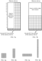
- the first error distribution area information is used in a case in which, when a data error occurs in a memory device, a specific area in which an error data bit falls in the memory device is the area in which the data error occurs, as shown in FIG. 5a .
- the second error distribution area information indicates that when a data error occurs in a memory device, a specific area in which an error data bit falls in the memory device is the area in which the data error occurs, as shown in FIG. 5b .
- the processing system determines, based on the second error distribution area information of the at least one memory space in the plurality of memory spaces, the second arrangement manner of the memory space occupied by the data symbol.
- the second arrangement manner of the memory space occupied by the data symbol matches an arrangement manner of the area indicated by the second error distribution area information.
- the second arrangement manner of the memory space occupied by the data symbol is strongly associated with the arrangement manner of the area indicated by the second error distribution area information.
- each data symbol occupies the 16-bit memory space.
- the processing system may set the second arrangement manner of the memory space occupied by the data symbol to the arrangement manner shown in FIG. 6c .
- step 307a may be performed before step 307.
- the processing system obtains the second error distribution area information of the at least one memory space in the plurality of memory spaces.
- the processing system may determine the second error distribution area information of the at least one memory space in the plurality of memory spaces based on a historical data error.
- the processing system may determine, with reference to the data error in a historical data reading result, a distribution area of data in which an error frequently occurs in the at least one memory space. Then, the processing system updates an error distribution area of the at least one memory space based on the distribution area of the data in which the error frequently occurs in the at least one memory space, to obtain the second error distribution area information of the at least one memory space.
- the error distribution area of the at least one memory space dynamically changes, and a reason why the error distribution area of the memory space dynamically changes is related to an operating environment, a business mode, and the like of the processing system.
- the operating environment includes an operating temperature of the processing system and an altitude of a place at which a device is located.
- the business mode includes frequent storage of data to specific locations during business processing.
- the processing system may update the error distribution area of the at least one memory space within a period of time with reference to the historical data error, to help maximize the error correction capability of the first ECC memory space of the first memory.
- Each of the P data symbols includes a plurality of data bits, and P is an integer greater than or equal to 1.
- Step 309 is similar to step 304. For details, refer to related descriptions of step 304.
- Step 310 is similar to step 305. For details, refer to related descriptions of step 305.
- the processing system writes the data bits included in the P data symbols and the redundant bits included in the Q first redundant symbols into the first memory.
- a specific arrangement manner of a memory space occupied by each symbol is shown in FIG. 11 .
- the arrangement manner of the memory space occupied by each symbol is arrangement in two rows and eight columns.
- step 310a further includes step 310a.
- Step 310a may be performed before step 310.
- Each of the P second redundant symbols includes at least one redundant bit, and P is an integer greater than or equal to 1.
- Step 310a may be similar to step 305a. For details, refer to related descriptions of step 310a.
- step 310 specifically includes: writing the P data symbols into the data memory space of the first memory, writing the Q first redundant symbols into the first ECC memory space of the first memory, and writing the Y second redundant symbols into the second ECC memory space of the first memory.
- the processing system may re-encode the data bits in all the data, to change the arrangement manner of the memory space occupied by the data symbol. This helps perform maximized error detection and maximized error correction on the data in a subsequent data reading process of the processing system, and the system reliability is improved.
- This application provides a data writing method.
- the method is applied to the processing system, the processing system includes the first memory, and the first memory includes the plurality of memory spaces.
- the method includes: obtaining the first data, where the first data is the data to be written into the first memory; determining, based on the first error distribution area information of the at least one memory space in the plurality of memory spaces, the first arrangement manner of the memory space occupied by the data symbol; determining the first data as the M data symbols based on the first arrangement manner of the memory space occupied by the data symbol, where each of the M data symbols includes the plurality of data bits, and M is the integer greater than or equal to 1; then performing ECC encoding on the M data symbols to obtain the N first redundant symbols, where each of the N first redundant symbols includes the at least one redundant bit, and N is the integer greater than or equal to 1; and writing the M data symbols into the data memory space of the first memory, and writing the N first redundant symbols into the first ECC memory space of the first memory.
- the processing system determines, based on the first error distribution area information of the at least one memory space in the plurality of memory spaces, the first arrangement manner of the memory space occupied by the data symbol. In other words, the processing system designs, with reference to distribution of error areas in the at least one memory space, the arrangement manner of the memory space occupied by the data symbol. Then, the processing system determines the first data as the M data symbols with reference to the first arrangement manner of the memory space occupied by the data symbol, where each of the M data symbols includes the data bits. Because destination addresses of the data bits in the first data are known, the processing system divides, with reference to the first arrangement manner, the data bits that are in the first data and that can form a shape of the first arrangement manner into a same data symbol.
- FIG. 12 is a schematic diagram of a structure of a processing system according to an embodiment of this application.
- the processing system includes a first memory, and the first memory includes a plurality of memory spaces.
- the processing system includes an obtaining unit 1201, a determining unit 1202, an encoding unit 1203, and a writing unit 1204.
- the processing system further includes a reading unit 1205.
- the obtaining unit 1201 is configured to obtain first data, where the first data is data to be written into the first memory.
- the determining unit 1202 is configured to: determine, based on first error distribution area information of at least one memory space in the plurality of memory spaces, a first arrangement manner of a memory space occupied by a data symbol; and determine the first data as M data symbols based on the first arrangement manner of the memory space occupied by the data symbol, where each of the M data symbols includes a plurality of data bits, and M is an integer greater than or equal to 1.
- the encoding unit 1203 is configured to perform first error correction code ECC encoding on the M data symbols to obtain N first redundant symbols, where each of the N first redundant symbols includes at least one redundant bit, and N is an integer greater than or equal to 1.
- the writing unit 1204 is configured to: write the M data symbols into a data memory space of the first memory, and write the N first redundant symbols into a first ECC memory space of the first memory.
- the first error distribution area information of the at least one memory space indicates a specific area, in the at least one memory space, in which an error data bit falls when a data error occurs in the at least one memory space.
- each data symbol occupies an 8-bit memory space
- the first arrangement manner of the memory space occupied by the data symbol includes any one of the following: arrangement in four rows and two columns, arrangement in two rows and four columns, arrangement in eight rows and one column, and arrangement in one row and eight columns; or
- the obtaining unit 1201 is further configured to: obtain the first error distribution area information of the at least one memory space in the plurality of memory spaces.
- the reading unit 1205 is configured to read all data from the first memory, where all the data includes data bits and a redundant bit.
- the determining unit 1202 is further configured to: determine, based on second error distribution area information of the at least one memory space in the plurality of memory spaces, a second arrangement manner of the memory space occupied by the data symbol; and determine the data bits in all the data as P data symbols based on the second arrangement manner of the memory space occupied by the data symbol, where each of the P data symbols includes a plurality of data bits, and P is an integer greater than or equal to 1.
- the encoding unit 1203 is further configured to: perform first ECC encoding on the P data symbols to obtain Q first redundant symbols, where each of the Q first redundant symbols includes at least one redundant bit, and Q is an integer greater than or equal to 1.
- the writing unit 1204 is further configured to: write the P data symbols into the data memory space of the first memory, and write the Q first redundant symbols into the first ECC memory space of the first memory.
- the obtaining unit 1201 is further configured to: obtain the second error distribution area information of the at least one memory space in the plurality of memory spaces.
- the obtaining unit 1201 is specifically configured to: determine the second error distribution area information of the at least one memory space in the plurality of memory spaces based on a historical data error.
- the data symbol and the first redundant symbol are RS code symbols; or the data symbol and the first redundant symbol are BCH code symbols.
- the first memory is an on die ECC memory.
- the encoding unit 1203 is specifically configured to: perform first ECC encoding on the M data symbols by using a finite field encoding algorithm to obtain the N first redundant symbols, where the finite field encoding algorithm includes an RS algorithm, a BCH algorithm, or the like.
- the first memory is a memory that supports second ECC encoding (for example, on die ECC), and the first memory further includes a second ECC memory space; and the encoding unit 1203 is further configured to: perform second ECC encoding on the M data symbols and the N first redundant symbols as data to obtain R second redundant symbols, where each of the R second redundant symbols includes at least one redundant bit, and R is an integer greater than or equal to 1.
- the writing unit 1204 is specifically configured to: write the M data symbols into the data memory space, write the N first redundant symbols into the first ECC memory space, and write the R second redundant symbols into the second ECC memory space.
- the processing system 1300 may include one or more central processing units (central processing units, CPUs) 1322 (for example, one or more processors), a storage 1332, and one or more storage media 1330 storing an application program 1342 or data 1344 (for example, one or more mass storage devices).
- CPUs central processing units
- storage 1332 for example, one or more storage devices
- application program 1342 or data 1344 for example, one or more mass storage devices
- the storage 1332 and the storage medium 1330 may be transient storage or persistent storage.
- the program stored in the storage medium 1330 may include one or more modules (not shown in the figure). Each module may include a series of instruction operations for the processing system. Further, the central processing unit 1322 may be configured to: communicate with the storage medium 1330, and perform, on the processing system 1300, the series of instruction operations in the storage medium 1330.
- the processing system 1300 may further include one or more power supplies 1326, one or more wired or wireless network interfaces 1350, one or more input/output interfaces 1358, and/or one or more operating systems 1341.
- the central processing unit 1322 is configured to perform the following solution:
- the first error distribution area information of the at least one memory space indicates a specific area, in the at least one memory space, in which an error data bit falls when a data error occurs in the at least one memory space.
- each data symbol occupies an 8-bit memory space
- the first arrangement manner of the memory space occupied by the data symbol includes any one of the following: arrangement in four rows and two columns, arrangement in two rows and four columns, arrangement in eight rows and one column, and arrangement in one row and eight columns; or
- the central processing unit 1322 is further configured to: obtain the first error distribution area information of the at least one memory space in the plurality of memory spaces.
- the central processing unit 1322 is further configured to:
- the central processing unit 1322 is further configured to: obtain the second error distribution area information of the at least one memory space in the plurality of memory spaces.
- the central processing unit 1322 is specifically configured to: determine the second error distribution area information of the at least one memory space in the plurality of memory spaces based on a historical data error.
- the data symbol and the first redundant symbol are RS code symbols; or the data symbol and the first redundant symbol are BCH code symbols.
- the first memory is an on die ECC memory.
- the central processing unit 1322 is specifically configured to: perform first ECC encoding on the M data symbols by using a finite field encoding algorithm to obtain the N first redundant symbols, where the finite field encoding algorithm includes an RS algorithm, a BCH algorithm, or the like.
- the first memory is a memory that supports second ECC encoding, and the first memory further includes a second ECC memory space; and the central processing unit 1322 is further configured to: perform second ECC encoding on the M data symbols and the N first redundant symbols as data to obtain R second redundant symbols, where each of the R second redundant symbols includes at least one redundant bit, and R is an integer greater than or equal to 1.
- the central processing unit 1322 is specifically configured to: write the M data symbols into the data memory space, write the N first redundant symbols into the first ECC memory space, and write the R second redundant symbols into the second ECC memory space.
- An embodiment of this application further provides a computer program product including instructions.
- the computer program product runs on a computer, the computer is enabled to perform the data writing method in embodiments shown in FIG. 3 .
- An embodiment of this application further provides a computer-readable storage medium, including computer instructions.
- the computer instructions When the computer instructions are run on a computer, the computer is enabled to perform the data writing method in embodiments shown in FIG. 3 .
- the chip when a processing system is a chip in a terminal, the chip includes a processing unit and a communication unit, where the processing unit may be, for example, a processor, and the communication unit may be, for example, an input/output interface, a pin, or a circuit.
- the processing unit may execute computer-executable instructions stored in a storage unit, so that the chip in the terminal performs the data writing method in embodiments shown in FIG. 3 .
- the storage unit is a storage unit in the chip, for example, a register or a cache.
- the storage unit may alternatively be a storage unit outside the chip in the terminal, for example, a read-only memory (read-only memory, ROM) or another type of static storage device that can store static information and instructions, or a random access memory (random access memory, RAM).
- ROM read-only memory
- RAM random access memory
- the processor mentioned in any of the foregoing may be a general central processing unit, a microprocessor, an application-specific integrated circuit (application-specific integrated circuit, ASIC), or one or more of integrated circuits configured to control program execution of the data writing method in embodiments shown in FIG. 3 .
- ASIC application-specific integrated circuit
- the disclosed system, apparatus, and method may be implemented in other manners.
- the described apparatus embodiment is merely an example.
- division into the units is merely logical function division and may be other division in actual implementation.
- a plurality of units or components may be combined or integrated into another system, or some features may be ignored or not performed.
- the displayed or discussed mutual couplings or direct couplings or communication connections may be implemented by using some interfaces.
- the indirect couplings or communication connections between the apparatuses or units may be implemented in electronic, mechanical, or other forms.
- the units described as separate parts may or may not be physically separate, and parts displayed as units may or may not be physical units, may be located in one position, or may be distributed on a plurality of network units. Some or all of the units may be selected based on actual requirements to achieve the objectives of the solutions of embodiments.
- functional units in embodiments of this application may be integrated into one processing unit, each of the units may exist alone physically, or two or more units are integrated into one unit.
- the integrated unit may be implemented in a form of hardware, or may be implemented in a form of a software functional unit.
- the integrated unit When the integrated unit is implemented in the form of the software functional unit and sold or used as an independent product, the integrated unit may be stored in a computer-readable storage medium.
- the computer software product is stored in a storage medium and includes several instructions for instructing a computer device (which may be a personal computer, a server, a network device, or the like) to perform all or some of the steps of the methods described in embodiments of this application.
- the foregoing storage medium includes any medium that can store program code, such as a USB flash drive, a removable hard disk, a ROM, a RAM, a magnetic disk, or an optical disc.
Landscapes
- Engineering & Computer Science (AREA)
- Theoretical Computer Science (AREA)
- Physics & Mathematics (AREA)
- General Engineering & Computer Science (AREA)
- General Physics & Mathematics (AREA)
- Quality & Reliability (AREA)
- Human Computer Interaction (AREA)
- Techniques For Improving Reliability Of Storages (AREA)
- Detection And Correction Of Errors (AREA)
Applications Claiming Priority (2)
| Application Number | Priority Date | Filing Date | Title |
|---|---|---|---|
| CN202210411764.4A CN116954982A (zh) | 2022-04-19 | 2022-04-19 | 数据写入方法以及处理系统 |
| PCT/CN2023/089083 WO2023202592A1 (zh) | 2022-04-19 | 2023-04-19 | 数据写入方法以及处理系统 |
Publications (2)
| Publication Number | Publication Date |
|---|---|
| EP4502809A1 true EP4502809A1 (de) | 2025-02-05 |
| EP4502809A4 EP4502809A4 (de) | 2025-08-13 |
Family
ID=88419202
Family Applications (1)
| Application Number | Title | Priority Date | Filing Date |
|---|---|---|---|
| EP23791247.2A Pending EP4502809A4 (de) | 2022-04-19 | 2023-04-19 | Datenschreibverfahren und verarbeitungssystem |
Country Status (4)
| Country | Link |
|---|---|
| US (1) | US20250045158A1 (de) |
| EP (1) | EP4502809A4 (de) |
| CN (2) | CN119003231B (de) |
| WO (1) | WO2023202592A1 (de) |
Families Citing this family (3)
| Publication number | Priority date | Publication date | Assignee | Title |
|---|---|---|---|---|
| CN117632579B (zh) * | 2024-01-25 | 2024-04-30 | 合肥兆芯电子有限公司 | 存储器控制方法和存储器存储装置 |
| CN120929420A (zh) * | 2024-05-11 | 2025-11-11 | 华为技术有限公司 | 内存模块、装置和服务器 |
| CN121217289A (zh) * | 2024-06-26 | 2025-12-26 | 海光信息技术股份有限公司 | 数据处理方法、装置及相关设备 |
Family Cites Families (16)
| Publication number | Priority date | Publication date | Assignee | Title |
|---|---|---|---|---|
| US5136592A (en) * | 1989-06-28 | 1992-08-04 | Digital Equipment Corporation | Error detection and correction system for long burst errors |
| US7620875B1 (en) * | 2006-03-07 | 2009-11-17 | Xilinx, Inc. | Error correction code memory system with a small footprint and byte write operation |
| KR20100094241A (ko) * | 2009-02-18 | 2010-08-26 | 삼성전자주식회사 | 예비 블록을 포함하지 않는 불휘발성 메모리 장치 |
| US8335970B2 (en) * | 2009-09-28 | 2012-12-18 | Broadcom Corporation | Encoder/decoder with unfolding error correction |
| US8640006B2 (en) * | 2011-06-29 | 2014-01-28 | International Business Machines Corporation | Preemptive memory repair based on multi-symbol, multi-scrub cycle analysis |
| US8935592B2 (en) * | 2012-11-20 | 2015-01-13 | Arm Limited | Apparatus and method for correcting errors in data accessed from a memory device |
| US9811420B2 (en) * | 2015-03-27 | 2017-11-07 | Intel Corporation | Extracting selective information from on-die dynamic random access memory (DRAM) error correction code (ECC) |
| US10331514B2 (en) * | 2017-03-17 | 2019-06-25 | Micron Technology, Inc. | Tiered error correction code (ECC) operations in memory |
| CN107068194A (zh) * | 2017-04-20 | 2017-08-18 | 聚辰半导体(上海)有限公司 | 一种应用在eeprom上的错误纠正编码及相应的eeprom |
| US11061930B1 (en) * | 2018-01-31 | 2021-07-13 | Amazon Technologies, Inc. | Dynamic management of storage object partitioning |
| KR102848706B1 (ko) * | 2018-12-24 | 2025-08-22 | 에스케이하이닉스 주식회사 | 메모리 시스템 및 메모리 모듈 |
| US11237902B2 (en) * | 2019-03-15 | 2022-02-01 | Innogrit Technologies Co., Ltd. | Systems and methods for an ECC architecture with memory mapping |
| CN112579342B (zh) * | 2020-12-07 | 2024-02-13 | 海光信息技术股份有限公司 | 内存纠错方法、内存控制器及电子设备 |
| CN113076219B (zh) * | 2021-04-27 | 2022-07-12 | 中国人民解放军国防科技大学 | 一种高能效的片上存储器错误检测与纠错电路及实现方法 |
| CN113485866B (zh) * | 2021-07-02 | 2023-05-09 | 海光信息技术股份有限公司 | 译码方法及相关装置、电子设备和存储介质 |
| US11687251B2 (en) * | 2021-09-28 | 2023-06-27 | Advanced Micro Devices, Inc. | Dynamic repartition of memory physical address mapping |
-
2022
- 2022-04-19 CN CN202410973654.6A patent/CN119003231B/zh active Active
- 2022-04-19 CN CN202210411764.4A patent/CN116954982A/zh active Pending
-
2023
- 2023-04-19 EP EP23791247.2A patent/EP4502809A4/de active Pending
- 2023-04-19 WO PCT/CN2023/089083 patent/WO2023202592A1/zh not_active Ceased
-
2024
- 2024-10-18 US US18/920,383 patent/US20250045158A1/en active Pending
Also Published As
| Publication number | Publication date |
|---|---|
| CN119003231A (zh) | 2024-11-22 |
| WO2023202592A1 (zh) | 2023-10-26 |
| US20250045158A1 (en) | 2025-02-06 |
| CN119003231B (zh) | 2025-06-24 |
| EP4502809A4 (de) | 2025-08-13 |
| CN116954982A (zh) | 2023-10-27 |
Similar Documents
| Publication | Publication Date | Title |
|---|---|---|
| USRE50830E1 (en) | Semiconductor memory devices including error correction circuits and methods of operating the semiconductor memory devices | |
| US11392454B2 (en) | Memory controllers, memory systems and memory modules | |
| US11681579B2 (en) | Semiconductor memory devices and memory systems including the same | |
| US10997020B2 (en) | Memory device, memory system, and method of operating the same | |
| JP5135348B2 (ja) | メモリ装置の信頼性、可用性、およびサービス性の改善 | |
| EP4502809A1 (de) | Datenschreibverfahren und verarbeitungssystem | |
| CN107430538B (zh) | 基于错误类型的ecc的动态应用 | |
| EP1449082B1 (de) | Fehlerkorrigierende speicher und verfahren zu seiner nutzung | |
| KR102190683B1 (ko) | 메모리 데이터 에러 정정 방법 | |
| US9064606B2 (en) | Memory interface supporting both ECC and per-byte data masking | |
| KR20210051668A (ko) | 메모리 컨트롤러, 메모리 시스템 및 메모리 모듈 | |
| JP2001249854A (ja) | メモリ設計のための共有式誤り訂正 | |
| CN116745849A (zh) | 存储器装置保护 | |
| US9627092B2 (en) | Semiconductor device performing error correction operation | |
| KR102633091B1 (ko) | 메모리 셀의 에러 확인 기능을 갖는 메모리 장치 및 이를 포함하는 메모리 모듈 | |
| US12411730B2 (en) | Memory system including data-width aware encoder and data-width aware decoder and operating method thereof | |
| US12271263B2 (en) | Semiconductor devices | |
| US20250013535A1 (en) | Data Writing Method and Processing System | |
| TWI864485B (zh) | 記憶體系統及其操作方法 |
Legal Events
| Date | Code | Title | Description |
|---|---|---|---|
| STAA | Information on the status of an ep patent application or granted ep patent |
Free format text: STATUS: THE INTERNATIONAL PUBLICATION HAS BEEN MADE |
|
| PUAI | Public reference made under article 153(3) epc to a published international application that has entered the european phase |
Free format text: ORIGINAL CODE: 0009012 |
|
| STAA | Information on the status of an ep patent application or granted ep patent |
Free format text: STATUS: REQUEST FOR EXAMINATION WAS MADE |
|
| 17P | Request for examination filed |
Effective date: 20241024 |
|
| AK | Designated contracting states |
Kind code of ref document: A1 Designated state(s): AL AT BE BG CH CY CZ DE DK EE ES FI FR GB GR HR HU IE IS IT LI LT LU LV MC ME MK MT NL NO PL PT RO RS SE SI SK SM TR |
|
| DAV | Request for validation of the european patent (deleted) | ||
| DAX | Request for extension of the european patent (deleted) | ||
| A4 | Supplementary search report drawn up and despatched |
Effective date: 20250710 |
|
| RIC1 | Information provided on ipc code assigned before grant |
Ipc: G06F 11/00 20060101AFI20250704BHEP |