EP4503337A2 - Connecteur pour composant électronique - Google Patents
Connecteur pour composant électronique Download PDFInfo
- Publication number
- EP4503337A2 EP4503337A2 EP24191664.2A EP24191664A EP4503337A2 EP 4503337 A2 EP4503337 A2 EP 4503337A2 EP 24191664 A EP24191664 A EP 24191664A EP 4503337 A2 EP4503337 A2 EP 4503337A2
- Authority
- EP
- European Patent Office
- Prior art keywords
- connector
- substrate
- terminals
- main body
- mounting
- Prior art date
- Legal status (The legal status is an assumption and is not a legal conclusion. Google has not performed a legal analysis and makes no representation as to the accuracy of the status listed.)
- Pending
Links
Images


Classifications
-
- H—ELECTRICITY
- H01—ELECTRIC ELEMENTS
- H01R—ELECTRICALLY-CONDUCTIVE CONNECTIONS; STRUCTURAL ASSOCIATIONS OF A PLURALITY OF MUTUALLY-INSULATED ELECTRICAL CONNECTING ELEMENTS; COUPLING DEVICES; CURRENT COLLECTORS
- H01R43/00—Apparatus or processes specially adapted for manufacturing, assembling, maintaining, or repairing of line connectors or current collectors or for joining electric conductors
- H01R43/02—Apparatus or processes specially adapted for manufacturing, assembling, maintaining, or repairing of line connectors or current collectors or for joining electric conductors for soldered or welded connections
- H01R43/0263—Apparatus or processes specially adapted for manufacturing, assembling, maintaining, or repairing of line connectors or current collectors or for joining electric conductors for soldered or welded connections for positioning or holding parts during soldering or welding process
-
- H—ELECTRICITY
- H01—ELECTRIC ELEMENTS
- H01R—ELECTRICALLY-CONDUCTIVE CONNECTIONS; STRUCTURAL ASSOCIATIONS OF A PLURALITY OF MUTUALLY-INSULATED ELECTRICAL CONNECTING ELEMENTS; COUPLING DEVICES; CURRENT COLLECTORS
- H01R4/00—Electrically-conductive connections between two or more conductive members in direct contact, i.e. touching one another; Means for effecting or maintaining such contact; Electrically-conductive connections having two or more spaced connecting locations for conductors and using contact members penetrating insulation
- H01R4/02—Soldered or welded connections
- H01R4/027—Soldered or welded connections comprising means for positioning or holding the parts to be soldered or welded
-
- H—ELECTRICITY
- H05—ELECTRIC TECHNIQUES NOT OTHERWISE PROVIDED FOR
- H05K—PRINTED CIRCUITS; CASINGS OR CONSTRUCTIONAL DETAILS OF ELECTRIC APPARATUS; MANUFACTURE OF ASSEMBLAGES OF ELECTRICAL COMPONENTS
- H05K1/00—Printed circuits
- H05K1/18—Printed circuits structurally associated with non-printed electric components
- H05K1/181—Printed circuits structurally associated with non-printed electric components associated with surface mounted components
-
- H—ELECTRICITY
- H05—ELECTRIC TECHNIQUES NOT OTHERWISE PROVIDED FOR
- H05K—PRINTED CIRCUITS; CASINGS OR CONSTRUCTIONAL DETAILS OF ELECTRIC APPARATUS; MANUFACTURE OF ASSEMBLAGES OF ELECTRICAL COMPONENTS
- H05K3/00—Apparatus or processes for manufacturing printed circuits
- H05K3/30—Assembling printed circuits with electric components, e.g. with resistors
- H05K3/32—Assembling printed circuits with electric components, e.g. with resistors electrically connecting electric components or wires to printed circuits
- H05K3/34—Assembling printed circuits with electric components, e.g. with resistors electrically connecting electric components or wires to printed circuits by soldering
- H05K3/3447—Lead-in-hole components
-
- H—ELECTRICITY
- H01—ELECTRIC ELEMENTS
- H01R—ELECTRICALLY-CONDUCTIVE CONNECTIONS; STRUCTURAL ASSOCIATIONS OF A PLURALITY OF MUTUALLY-INSULATED ELECTRICAL CONNECTING ELEMENTS; COUPLING DEVICES; CURRENT COLLECTORS
- H01R12/00—Structural associations of a plurality of mutually-insulated electrical connecting elements, specially adapted for printed circuits, e.g. printed circuit boards [PCB], flat or ribbon cables, or like generally planar structures, e.g. terminal strips, terminal blocks; Coupling devices specially adapted for printed circuits, flat or ribbon cables, or like generally planar structures; Terminals specially adapted for contact with, or insertion into, printed circuits, flat or ribbon cables, or like generally planar structures
- H01R12/50—Fixed connections
- H01R12/51—Fixed connections for rigid printed circuits or like structures
- H01R12/55—Fixed connections for rigid printed circuits or like structures characterised by the terminals
- H01R12/57—Fixed connections for rigid printed circuits or like structures characterised by the terminals surface mounting terminals
-
- H—ELECTRICITY
- H05—ELECTRIC TECHNIQUES NOT OTHERWISE PROVIDED FOR
- H05K—PRINTED CIRCUITS; CASINGS OR CONSTRUCTIONAL DETAILS OF ELECTRIC APPARATUS; MANUFACTURE OF ASSEMBLAGES OF ELECTRICAL COMPONENTS
- H05K2201/00—Indexing scheme relating to printed circuits covered by H05K1/00
- H05K2201/09—Shape and layout
- H05K2201/09009—Substrate related
- H05K2201/09027—Non-rectangular flat PCB, e.g. circular
-
- H—ELECTRICITY
- H05—ELECTRIC TECHNIQUES NOT OTHERWISE PROVIDED FOR
- H05K—PRINTED CIRCUITS; CASINGS OR CONSTRUCTIONAL DETAILS OF ELECTRIC APPARATUS; MANUFACTURE OF ASSEMBLAGES OF ELECTRICAL COMPONENTS
- H05K2201/00—Indexing scheme relating to printed circuits covered by H05K1/00
- H05K2201/10—Details of components or other objects attached to or integrated in a printed circuit board
- H05K2201/10007—Types of components
- H05K2201/10189—Non-printed connector
-
- H—ELECTRICITY
- H05—ELECTRIC TECHNIQUES NOT OTHERWISE PROVIDED FOR
- H05K—PRINTED CIRCUITS; CASINGS OR CONSTRUCTIONAL DETAILS OF ELECTRIC APPARATUS; MANUFACTURE OF ASSEMBLAGES OF ELECTRICAL COMPONENTS
- H05K2201/00—Indexing scheme relating to printed circuits covered by H05K1/00
- H05K2201/10—Details of components or other objects attached to or integrated in a printed circuit board
- H05K2201/10227—Other objects, e.g. metallic pieces
- H05K2201/10295—Metallic connector elements partly mounted in a hole of the PCB
- H05K2201/10303—Pin-in-hole mounted pins
-
- H—ELECTRICITY
- H05—ELECTRIC TECHNIQUES NOT OTHERWISE PROVIDED FOR
- H05K—PRINTED CIRCUITS; CASINGS OR CONSTRUCTIONAL DETAILS OF ELECTRIC APPARATUS; MANUFACTURE OF ASSEMBLAGES OF ELECTRICAL COMPONENTS
- H05K2201/00—Indexing scheme relating to printed circuits covered by H05K1/00
- H05K2201/10—Details of components or other objects attached to or integrated in a printed circuit board
- H05K2201/10431—Details of mounted components
- H05K2201/10606—Permanent holder for component or auxiliary printed circuits mounted on a printed circuit board [PCB]
Definitions
- a variety of techniques to connect electronic components to a substrate, such as a PCB, is known.
- pins (or terminals) from the electronic components are passed through holes preformed in the substrate.
- the pins are then bent and fixed to the substrate, for instance, by means of soldering.
- the electronic component is held by a holding tool so that the pins may be soldered. If not held reliably, there is possibility of slippage of the pins during soldering.
- the technical problem to be solved by the present subject matter is how to provide a connector that facilitate an efficient connection of electronic components to a substrate, ensuring mounting of the electronic component to be simple and involves fewer processes, whilst maintaining the structural integrity of the electronic component(s) and the connection.
- the present subject matter seeks to solve the above-mentioned technical problem in conventional connectors of electronic components.
- Such connectors may be applied to connect electronic components to a substrate for use in automotive applications.
- the application is not limited to automotive applications alone.
- the present subject matter relates to a connector comprising: a main body having a substantially rectangular profile and comprising: a front face and a bottom face parallel to one another and a lateral face there-between; a plurality of passages adapted to receive terminals of an electronic component; and at least two mounting legs projecting perpendicularly from the front face of the main body, each of said mounting legs comprising a detent shoulder extending outwardly and defining a contact surface directed towards the front face of the main body. Accordingly, upon mounting the connector onto a substrate, such as a PCB, the at least two mounting legs facilitate the connector to a snap fit, or press fit, to said substrate.
- a substrate such as a PCB
- the present subject matter relates also to an electrical device comprising: a substrate defining a top surface, a bottom surface, and an electric circuit printed in at least the top surface; and a connector, configured in accordance with the foregoing description, mounted on the bottom surface of the substrate, wherein terminals of an electronic component is received through the plurality of passages.
- electronic components in such an electric device may be mounted to the substrate in a simple and cost effective manner since a dedicated tool to hold the terminals is not required while connecting the terminals to the electric circuit.
- the connector is fixed in a robust manner to restrict axial and lateral play, thereby ensuring structural integrity of the connection between the electronic component to the electric circuit.
- the present subject matter relates also to a method of assembling the electrical device, the method comprising: placing the terminals of the electronic component against a placement surface of the first part, the placement surface being lateral to the front face and the bottom face; placing the second part on the terminals and sandwiching said terminals between the first part and the second part; fusing the second part into the first part for fixture of the terminals to the connector; and mounting the connector to the bottom surface of the substrate, said step of mounting comprising: inserting the at least two mounting legs into a hole formed on the substrate so that the contact surface of the detent shoulder comes in contact with the top surface of the substrate.
- the step of mounting the connector to the bottom surface further comprises the second contact surface coming in contact with the bottom surface of the substrate.
- FIG. 1 illustrates a connector 100, configured in accordance with the present subject matter.
- the connector 100 includes a main body 102 and at least two mounting legs 112.
- the main body 102 has a substantially rectangular profile and includes a front face 104 and a bottom face 106 parallel to one another. Further, between the aforementioned two flat faces 104, 106, that is, the front face 104 and the bottom face 106, is a lateral face 108 formed there-between.
- the main body 102 further includes a plurality of passages adapted to receive terminals 116 of an electronic component 114.
- the at least two mounting legs 112 project perpendicularly from the front face 104.
- Each of the mounting legs 112 include a detent shoulder extending outwardly. The detent shoulder defines a contact surface that is directed towards the front face 104 of the main body 102.
- FIG. 2A illustrates a perspective view of the connector 100, configured in accordance with the present subject matter, in which the electronic component 114 is excluded.
- FIG. 2B illustrates another perspective view of the connector 100 excluding the electronic component 114.
- the description provided herein pertains to FIG.s 2A and 2B in tandem.
- FIG. 2A and 2B depicts the main body 102 and plurality of passages 200 formed there-through.
- the plurality of passages 200 permit terminals 114 of the electronic component 114 through the main body 102.
- the terminals 114 pass into the plurality of passages 200 from the bottom face 106 and exit from the front face 104.
- mounting legs 112, formed on the front face 104 is provided on both sides of the plurality of passages 200.
- the mounting leg 112 with two leg portions 112a, 112b is formed in a substantially cylindrical manner.
- Each of the two mounting legs 112 may include one or more leg portions 112a, 112b, 112c.
- a detent shoulder 204a, 204b, 204c is formed on each of the at least two mounting legs 112.
- the connector 100 includes two mounting legs 112. one of the two mounting legs 112 is split into two leg portions 112a and 112b; and therefore for each of said leg portions 112a and 112b, there is one detent shoulder 204a and 204b respectively.
- the other mounting leg 112 includes just one leg portion 112c for which the detent shoulder 204c if formed thereof.
- Each detent shoulder 204a, 204b, 204c defines a contact surface 206.
- the contact surface 206 on each detent shoulder 204a, 204b, 204c faces the front face 104 of the main body 102.
- the orientation of the detent shoulders 204a, 204b, 204c is such that the contact surfaces 206 are parallel to the front face 104 of the main body 102. Therefore, upon mounting the connector 100 to a substrate, the orientation of the contact surfaces 206 and the front face 106 is such that said substrate is disposed there-between.
- the detent shoulders 204a, 204b, 204c are formed in an arcuate shape. Such a shape defines a smooth curved surface on the detent shoulders 204a, 204b, 204c that facilitate easy passing through of said shoulders 204a, 204b, 204c through a hole in a substrate.
- the connector 100 further includes at least one flange 201 that extend from the lateral face 108 of the main body 102.
- the at least one flange 201 defines a second contact surface 202 parallel to the two flat faces, the two flat faces being the front face 104 and the bottom face 106 of the main body 102.
- the second contact surface 202 is oriented to be parallel to the contact surface 206 of the detent shoulders 204a, 204b, 204c.
- the connector 100 may include several flanges 201 distant from each other. In the example figures, there are three flanges 201, each having the second contact surface 202 oriented to face the contact surface 206 of the detent shoulder.
- the mounting leg 112 that is split into two leg portions 112a, 112b, there is a dedicated flange 202.
- the mounting 112 that has only one leg portion 112c, there are two flanges 202.
- the flanges 202 are oriented so that the second contact surface 202 is facing the contact surface 206. Accordingly, upon mounting the connector 100 to a substrate, the substrate is sandwiched between the contact surface 206 and the second contact surface 206.
- the leg portions 112a and 112b that are arranged in opposite directions is separated by a hole 208.
- a hole 208 separates the two leg portions 112a, 112b and also provides flexibility for the leg portions 112a and 112b to bend towards each other.
- FIG. 3A illustrates the connector 100 mounted on a substrate 302, configured in accordance with an example of the present subject matter.
- FIG. 3B is a zoomed in view of the connector 100 mounted on the substrate 302, at 310 from FIG. 3A.
- Figure 3C illustrates an electrical device 300 in which the connector 100 is applied, configured in accordance with an example of the present subject matter.
- FIG. 3D is a sectional view of the electrical device 300, in accordance with the example shown in FIG. 3C .
- FIG. 3E is a zoomed in view of the connector 100 mounted on the substrate 302 of the electrical device, in accordance with the example shown in FIG. 3C .
- the description that follows pertain to FIG.s 3A, 3B, 3C , 3D and 3E in tandem.
- the connector 100 is mounted on a substrate 302, as shown in FIG. 3A .
- the detent shoulders 204a, 204b, 204c is passed through a hole 308 in the substrate 302 and exits from another side of the substrate 302.
- the substrate 302 is a printed circuit board (PCB) where an electric circuit is integrated on at least one side of the PCB.
- the second contact surface 206 abuts a surface of the substrate 302 from which the detent shoulders 204a, 204b, 204c enters through the hole 308.
- the connector 100 may be used as an interconnector (not shown), wherein the plurality of passages 200 are configured to fix interconnecting pins therein.
- interconnecting pins may be male or female type pins that facilitate transfer of electric current or signals between two electrical devices, for instance, between an electric power converter and a DC-DC converter.
- a connector 100 functioning as an interconnector, may be mounted on a PCB within an electrical device, such as, an electric power converter, a DC-DC converter, or a battery pack.
- the present subject matter also relates to an electrical device 300 that includes the substrate 302 and the connector 100 as described above.
- the electric device 300 is an electric power converter for conversion of electric current from alternating current (AC) to direct current (DC) and/or vice-versa.
- the substrate 302 has a top surface 304, a bottom surface 306, and an electric circuit (not depicted).
- the electric circuit is printed in at least the top surface 304 of the substrate 302.
- the connector 100 formed in the manner described above, is mounted from the bottom surface 306 of the substrate 302. Accordingly, terminals 116 of the electronic component 114 is received through the plurality of passages 200 formed in the connector 100.
- An electric connection between the electronic component 114 and the electric circuit of the substrate 302 may be achieved for an effective conversion of AC to DC and/or vice-versa.
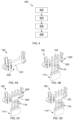
- FIG. 4 illustrates a flowchart for a method 400 of assembling the electrical device 300, namely, the connector 100, the electronic component 114, and the substrate 302 together.
- FIG. 5A, 5B, 5C, and 5D illustrates a step-by-step approach to assembling together the aforementioned components.
- FIG.s 5A, 5B, 5C and 5D The description that follows therefore pertain to the aforementioned figures in tandem.
- the connector 100 includes the main body 102.
- the main body 102 is preformed and the terminals 116 of the electronic component 114 is passed through the plurality of passages 200.
- the main body 102 is formed from two parts fused together with the terminals 116 being placed in between said two parts.
- FIG. 5A through 5D illustrates one such example where the main body 102 is formed from two parts.
- FIG. 5A illustrates a first part 500 of the two parts forming the main body 102.
- a second part 504 of said two parts is shown in FIG. 5C .
- the method 400 further includes a step 404 of placing the second part 504 on the terminals 116 so that the terminals 116 are sandwiched between the first part 500 and the second part 504, as depicted in FIG. 5C .
- the method 400 further includes a step 406 of fusing the second part 504 to the first part 500 of the connector 100.
- a fusing process such as, ultrasonic riveting
- the second part 504 is fused to the first part 500 thereby ensuring the terminals 116 are fixed, or assembled, to the connector 100.
- the connector 100 is formed of electrically insulating material, that is, the first part 500 and the second part 504 are formed from electrically insulating material; and, said parts 500, 504 brought in close proximity together, with the terminals sandwiched there-between, and melted by an application of heat or the like.
- the method 400 furthermore includes a step 408 of mounting the connector 100 to the bottom surface 306 of the substrate 302.
- the aforementioned step 408 of mounting includes inserting the at least two mounting legs 112 into the hole 308 formed on the substrate 302. More particularly, the one or more leg portions 112a, 112b, 112c is inserted through the hole 308.
- the insertion step in 408 is performed from when the detent shoulders 204a, 204b, 204c enters the substrate 302 from the bottom surface 306 and exits the top surface 304 via the hole 302. Accordingly, the contact surface 206 comes in contact with the top surface 304 of the substrate 302.
- the step 408 of inserting the leg portions 112a, 112b, 112c is performed till such a time the second contact surface 202 comes in contact with the bottom surface 306 of the substrate 302.
- the outcome configuration of the aforementioned step 408 of mounting the connector 100 to the substrate 302 is depicted in FIG. 3A and 3B .
- Such a substrate 302 may be a PCB of an electric power converter such as the one depicted in FIG. 3C , 3D and 3D .
- the connector 100 In the example where the electronic component 114 is a capacitor (or any other example electronic component 114 of the like) and the substrate 302 is a PCB, the connector 100, with the electronic component 114 fixed therein, the connector 100 is mounted onto the PCB in step 408.
- the second contact surface 202 of the at least one flange 201 come in contact with the bottom surface 306 of the PCB; and the contact surface(s) 206 of the detent shoulder(s) 204a, 204b, 204c come in contact with the opposite surface, i.e., the top surface 304, from which the detent shoulder(s) 204a, 204b, 204c exit.
- a stable mounting of the capacitor is achieved accordingly. Any axial and lateral play of the connector 100, and hence, the terminals 116 of the capacitor, is also largely mitigated. A process requiring holding the terminals of the capacitor for soldering is also eliminated.
Landscapes
- Engineering & Computer Science (AREA)
- Microelectronics & Electronic Packaging (AREA)
- Manufacturing & Machinery (AREA)
- Details Of Connecting Devices For Male And Female Coupling (AREA)
- Coupling Device And Connection With Printed Circuit (AREA)
Applications Claiming Priority (1)
| Application Number | Priority Date | Filing Date | Title |
|---|---|---|---|
| IN202341051782 | 2023-08-01 |
Publications (2)
| Publication Number | Publication Date |
|---|---|
| EP4503337A2 true EP4503337A2 (fr) | 2025-02-05 |
| EP4503337A3 EP4503337A3 (fr) | 2025-04-02 |
Family
ID=92142046
Family Applications (1)
| Application Number | Title | Priority Date | Filing Date |
|---|---|---|---|
| EP24191664.2A Pending EP4503337A3 (fr) | 2023-08-01 | 2024-07-30 | Connecteur pour composant électronique |
Country Status (1)
| Country | Link |
|---|---|
| EP (1) | EP4503337A3 (fr) |
Citations (1)
| Publication number | Priority date | Publication date | Assignee | Title |
|---|---|---|---|---|
| CN114172387A (zh) | 2020-09-11 | 2022-03-11 | 采埃孚股份公司 | 制造逆变器的方法以及定位辅助装置和逆变器 |
Family Cites Families (4)
| Publication number | Priority date | Publication date | Assignee | Title |
|---|---|---|---|---|
| US5344338A (en) * | 1992-03-04 | 1994-09-06 | Molex Incorporated | Strain relief structure for connecting flat flexible cable to a circuit board |
| GB2328329A (en) * | 1997-08-13 | 1999-02-17 | Ford Motor Co | Guiding pins for an electrical connection |
| EP3641067A1 (fr) * | 2018-10-19 | 2020-04-22 | Quan Mei Technology Co. Ltd | En-tête de broche |
| JP7155987B2 (ja) * | 2018-12-14 | 2022-10-19 | 住友電装株式会社 | ハーネス部品 |
-
2024
- 2024-07-30 EP EP24191664.2A patent/EP4503337A3/fr active Pending
Patent Citations (1)
| Publication number | Priority date | Publication date | Assignee | Title |
|---|---|---|---|---|
| CN114172387A (zh) | 2020-09-11 | 2022-03-11 | 采埃孚股份公司 | 制造逆变器的方法以及定位辅助装置和逆变器 |
Also Published As
| Publication number | Publication date |
|---|---|
| EP4503337A3 (fr) | 2025-04-02 |
Similar Documents
| Publication | Publication Date | Title |
|---|---|---|
| US7140885B2 (en) | Housing case for electronic circuit board | |
| US5254016A (en) | Interconnect device mounting apparatus for printed circuit boards | |
| US6080008A (en) | Push-wire contact | |
| CN105144433A (zh) | 用于制造电池接触系统的方法以及电池接触系统 | |
| JP2003257524A (ja) | 電気コネクタ | |
| US20100144177A1 (en) | Electrical connector with interlocking features | |
| US20230017724A1 (en) | High voltage contact system | |
| US20010010626A1 (en) | Substrate mount type terminal | |
| CN101305500A (zh) | 带有可分开的结合部的印刷电路板堆叠连接件 | |
| US9407021B2 (en) | Compound cylinder PCB connection | |
| US20030060087A1 (en) | Terminal and connector using same | |
| EP4503337A2 (fr) | Connecteur pour composant électronique | |
| US8480412B2 (en) | Terminal and connector assembly | |
| KR20190048538A (ko) | 기판 접속용 커넥터 | |
| TWI333304B (en) | Ic socket | |
| EP0899830A2 (fr) | Connecteur pour carte à circuits avec une base composée isolante | |
| JPH10255930A (ja) | 電気コネクタ | |
| JP2002299000A (ja) | 可撓性プリント基板と接続端子の接合方法 | |
| JPH07161441A (ja) | 表面実装型コネクタ及びその製造方法 | |
| US20120129363A1 (en) | Electrical connector | |
| CN207338827U (zh) | 连接器 | |
| TWI275206B (en) | Electrical connector | |
| JPH1126048A (ja) | 端子具 | |
| US12581588B2 (en) | Press-fit fasteners for securing components together | |
| JP2003032840A (ja) | 電気接続箱 |
Legal Events
| Date | Code | Title | Description |
|---|---|---|---|
| PUAI | Public reference made under article 153(3) epc to a published international application that has entered the european phase |
Free format text: ORIGINAL CODE: 0009012 |
|
| STAA | Information on the status of an ep patent application or granted ep patent |
Free format text: STATUS: REQUEST FOR EXAMINATION WAS MADE |
|
| 17P | Request for examination filed |
Effective date: 20240730 |
|
| AK | Designated contracting states |
Kind code of ref document: A2 Designated state(s): AL AT BE BG CH CY CZ DE DK EE ES FI FR GB GR HR HU IE IS IT LI LT LU LV MC ME MK MT NL NO PL PT RO RS SE SI SK SM TR |
|
| PUAL | Search report despatched |
Free format text: ORIGINAL CODE: 0009013 |
|
| AK | Designated contracting states |
Kind code of ref document: A3 Designated state(s): AL AT BE BG CH CY CZ DE DK EE ES FI FR GB GR HR HU IE IS IT LI LT LU LV MC ME MK MT NL NO PL PT RO RS SE SI SK SM TR |
|
| RIC1 | Information provided on ipc code assigned before grant |
Ipc: H01R 43/02 20060101ALI20250225BHEP Ipc: H05K 3/34 20060101ALI20250225BHEP Ipc: H01R 12/57 20110101ALI20250225BHEP Ipc: H01R 4/02 20060101AFI20250225BHEP |