EP4505943A1 - Carte de circuit imprimé pour un système d'imagerie - Google Patents
Carte de circuit imprimé pour un système d'imagerie Download PDFInfo
- Publication number
- EP4505943A1 EP4505943A1 EP23191117.3A EP23191117A EP4505943A1 EP 4505943 A1 EP4505943 A1 EP 4505943A1 EP 23191117 A EP23191117 A EP 23191117A EP 4505943 A1 EP4505943 A1 EP 4505943A1
- Authority
- EP
- European Patent Office
- Prior art keywords
- circuit board
- imaging system
- mesh
- signal line
- holes
- Prior art date
- Legal status (The legal status is an assumption and is not a legal conclusion. Google has not performed a legal analysis and makes no representation as to the accuracy of the status listed.)
- Pending
Links
Images



Classifications
-
- A—HUMAN NECESSITIES
- A61—MEDICAL OR VETERINARY SCIENCE; HYGIENE
- A61B—DIAGNOSIS; SURGERY; IDENTIFICATION
- A61B6/00—Apparatus or devices for radiation diagnosis; Apparatus or devices for radiation diagnosis combined with radiation therapy equipment
- A61B6/56—Details of data transmission or power supply, e.g. use of slip rings
-
- A—HUMAN NECESSITIES
- A61—MEDICAL OR VETERINARY SCIENCE; HYGIENE
- A61B—DIAGNOSIS; SURGERY; IDENTIFICATION
- A61B5/00—Measuring for diagnostic purposes; Identification of persons
- A61B5/0033—Features or image-related aspects of imaging apparatus, e.g. for MRI, optical tomography or impedance tomography apparatus; Arrangements of imaging apparatus in a room
- A61B5/0035—Features or image-related aspects of imaging apparatus, e.g. for MRI, optical tomography or impedance tomography apparatus; Arrangements of imaging apparatus in a room adapted for acquisition of images from more than one imaging mode, e.g. combining MRI and optical tomography
-
- A—HUMAN NECESSITIES
- A61—MEDICAL OR VETERINARY SCIENCE; HYGIENE
- A61B—DIAGNOSIS; SURGERY; IDENTIFICATION
- A61B5/00—Measuring for diagnostic purposes; Identification of persons
- A61B5/05—Detecting, measuring or recording for diagnosis by means of electric currents or magnetic fields; Measuring using microwaves or radio waves
- A61B5/055—Detecting, measuring or recording for diagnosis by means of electric currents or magnetic fields; Measuring using microwaves or radio waves involving electronic [EMR] or nuclear [NMR] magnetic resonance, e.g. magnetic resonance imaging
-
- A—HUMAN NECESSITIES
- A61—MEDICAL OR VETERINARY SCIENCE; HYGIENE
- A61B—DIAGNOSIS; SURGERY; IDENTIFICATION
- A61B6/00—Apparatus or devices for radiation diagnosis; Apparatus or devices for radiation diagnosis combined with radiation therapy equipment
- A61B6/44—Constructional features of apparatus for radiation diagnosis
- A61B6/4417—Constructional features of apparatus for radiation diagnosis related to combined acquisition of different diagnostic modalities
-
- A—HUMAN NECESSITIES
- A61—MEDICAL OR VETERINARY SCIENCE; HYGIENE
- A61B—DIAGNOSIS; SURGERY; IDENTIFICATION
- A61B2562/00—Details of sensors; Constructional details of sensor housings or probes; Accessories for sensors
- A61B2562/16—Details of sensor housings or probes; Details of structural supports for sensors
- A61B2562/166—Details of sensor housings or probes; Details of structural supports for sensors the sensor is mounted on a specially adapted printed circuit board
-
- A—HUMAN NECESSITIES
- A61—MEDICAL OR VETERINARY SCIENCE; HYGIENE
- A61B—DIAGNOSIS; SURGERY; IDENTIFICATION
- A61B2562/00—Details of sensors; Constructional details of sensor housings or probes; Accessories for sensors
- A61B2562/18—Shielding or protection of sensors from environmental influences, e.g. protection from mechanical damage
- A61B2562/182—Electrical shielding, e.g. using a Faraday cage
-
- A—HUMAN NECESSITIES
- A61—MEDICAL OR VETERINARY SCIENCE; HYGIENE
- A61B—DIAGNOSIS; SURGERY; IDENTIFICATION
- A61B6/00—Apparatus or devices for radiation diagnosis; Apparatus or devices for radiation diagnosis combined with radiation therapy equipment
- A61B6/02—Arrangements for diagnosis sequentially in different planes; Stereoscopic radiation diagnosis
- A61B6/03—Computed tomography [CT]
- A61B6/037—Emission tomography
-
- H—ELECTRICITY
- H05—ELECTRIC TECHNIQUES NOT OTHERWISE PROVIDED FOR
- H05K—PRINTED CIRCUITS; CASINGS OR CONSTRUCTIONAL DETAILS OF ELECTRIC APPARATUS; MANUFACTURE OF ASSEMBLAGES OF ELECTRICAL COMPONENTS
- H05K1/00—Printed circuits
- H05K1/02—Details
- H05K1/0213—Electrical arrangements not otherwise provided for
- H05K1/0237—High frequency adaptations
- H05K1/025—Impedance arrangements, e.g. impedance matching, reduction of parasitic impedance
- H05K1/0253—Impedance adaptations of transmission lines by special lay-out of power planes, e.g. providing openings
-
- H—ELECTRICITY
- H05—ELECTRIC TECHNIQUES NOT OTHERWISE PROVIDED FOR
- H05K—PRINTED CIRCUITS; CASINGS OR CONSTRUCTIONAL DETAILS OF ELECTRIC APPARATUS; MANUFACTURE OF ASSEMBLAGES OF ELECTRICAL COMPONENTS
- H05K2201/00—Indexing scheme relating to printed circuits covered by H05K1/00
- H05K2201/07—Electric details
- H05K2201/0776—Resistance and impedance
- H05K2201/0792—Means against parasitic impedance; Means against eddy currents
Definitions
- the invention relates to an imaging system, a circuit board for an imaging system, and a method for designing a circuit board arrangement.
- Imaging systems in which magnetic resonance imaging (MRI) is combined with other imaging modalities, such as with positron emission tomography (PET), provide additional diagnostic possibilities. For example, images with the different modalities may be taken simultaneously or nearly simultaneously and without repositioning a subject, such as a patient, in between taking images.
- MRI systems create magnetic fields, in particular magnetic gradient fields, with high field strength that change quickly over time. Therefore, electrically conductive materials that are positioned within the magnetic field of the MRI system may heat up due to eddy currents that are induced by the rapidly varying magnetic gradient field.
- electronics of the other imaging modality e.g.
- PET electronics usually including printed circuit boards, often have to be placed close to the gradient coils of the MRI system. In this position, field components of the MRI magnetic gradient field perpendicular to the z-axis of the MRI system are relatively large. Since the PET electronics necessarily comprise conductive materials, such as copper layers, and their design is restricted by requirements of the PET system itself, eddy currents are induced in the PET electronics leading to heating of the electronics. This, in turn, may lead to various problems such as a temperature-dependent drift of the PET signal, a reduction of the lifetime or complete destruction of temperature-sensitive components, a (partial) detachment of components of printed circuit boards, or a requirement to replace detector elements. Furthermore, the induced eddy currents can cause image quality problems such as echo-planar imaging (EPI) ghosting.
- EPI echo-planar imaging
- One possible measure is to maximize the impedance in the frequency range of the eddy currents (typically kHz) while, at the same time, keeping it small in the frequency range of the clock (typically in the range of MHz to GHz).
- the frequency range of the clock typically in the range of MHz to GHz.
- capacitive segmentation of the shield e.g. with discrete components and/or by laminating capacitances.
- the achievable areal capacitance is limited by the minimum substrate thickness of the dielectric layer and its dielectric constant and additional components, such as additional discrete components, cause additional costs.
- a practical implementation of these measure requires space, which is limited due to the MRI components.
- an imaging system in particular medical imaging system, comprises a magnetic resonance imaging system with a gradient coil arrangement configured to produce a varying magnetic gradient field during operation.
- the medical imaging system comprises one or several printed circuit boards arranged such that they are within the magnetic gradient field of the magnetic resonance imaging system during operation, each circuit board having at least one conducting layer, in particular a copper layer, wherein at least one of the circuit boards comprises a mesh of holes that spreads over at least a partial region of the conducting layer.
- the imaging system may comprise at least one further imaging modality.
- the one or several printed circuit boards may be part of the at least one further imaging modality.
- the one or several printed circuit boards may be part of the magnetic resonance imaging system or of any other electronics of the whole imaging system.
- the several circuit boards are part of a stack of circuit boards.
- the at least one circuit board may comprise a stack of layers.
- the mesh of holes can increase the impedance of the conducting layer, at least in the region of the mesh.
- the mesh of holes may be configured to increase the impedance of the circuit board in the kHz range. It has been found that this range may be particularly relevant for the purpose of eddy current induced heating due to the changing magnetic fields.
- the mesh of holes may have a similar effect as physically decreasing the thickness of the conducting layer.
- a mesh of holes can be an easy to manufacture and surprisingly efficient way of decreasing the induction of heat in the circuit board.
- the provision of the mesh does not require additional discrete components or additional space in order to reduce the heating.
- the arrangement or placement of the mesh can be easily adapted corresponding to the individual needs depending on the function a design of the circuit board. This may for example, be particularly beneficial for designing sensitive circuit areas.
- the inventive solution may thus provide a flexible and adaptable way of reducing the heat induction.
- the one or several printed circuit boards may be part of the electronics of the imaging system. Since providing the mesh of holes can reduce a heating induced by changing magnetic fields, the design of the imaging system and its electronics can be more flexible. Usually, the magnetic resonance imaging system and its magnetic fields restrict the placement of circuit boards or requires measures of shielding the corresponding electronics or other measures to reduce an induction of currents due to the magnetic fields. There often is a competition of trying to place the electronics in an area where the magnetic fields are as low as possible, on the one hand, and, on the other hand, having only limited space available in these areas as well as actually wanting the electronics to be close to a subject or object that is examined for various reasons. Due to the mesh, a greater flexibility can be achieved with regard to the circuit board placement.
- the term "within the magnetic gradient field” may in particular mean, that the position of the circuit board is in an area where, during operation, the magnetic fields or the variation of the magnetic field, is higher than a thousandth, preferably higher than a hundredth, of the maximum value of the magnetic fields or the variation of the magnetic field.
- the circuit board may be positioned inside the gradient coil of the magnetic resonance imaging system.
- the circuit board may, for example, be arranged around an examination area, where an object or subject, such as a patient, is to be examined.
- the at least one circuit board is not elastic.
- the at least one circuit board may have an elasticity value defined by a Young's modulus of more than 15 Gpa, preferably more than 20 Gpa. It may be provided that the circuit board is installed in the imaging system without being flexed or bended for a substantial amount.
- the printed circuit not being flexed or bended may provide more freedom in designing the circuit board, since, for example, a flexible printed circuit may have to be designed such that a bending is not detrimental to the function of the circuit board.
- the imaging system further comprises a positron emission tomography (PET) system, wherein the at least one circuit board is part of the electronics of the positron emission tomography system.
- PET positron emission tomography
- the inventive system may be particularly advantageous, when the at least one printed circuit board is part of a PET system.
- a further particular advantage with respect to this embodiment can be, that the mesh tends to increase the impedance in the kHz range but keep the impedance low enough for PET specific purposes. At least some parts of the PET electronics, usually operate at higher frequencies that are not affected negatively as much.
- the impedance of the circuit board due to the mesh may still be low enough at the higher frequencies required for (at least some of) the PET electronics.
- the invention can be particularly advantageous for a PET system, the invention can generally also be used for any other type of electronics.
- the other type of electronics can be part of the MRI system or of another imaging modality or of any other electronic component.
- the at least one circuit board comprises at least one electronic signal line running across the mesh. It has been found that, surprisingly, the impact of the mesh of holes on the signal quality of the signal line can often be low enough that it is still feasible without significantly impeding the overall functionality of the electronics the circuit board is a part of.
- the at least one circuit board comprises a trace of conducting material running across the mesh and following the course of the at least one signal line, wherein the trace of conducting material is wider than the at least one signal line, such that, at least across the mesh, the at least one signal line is widened by the trace of conducting material.
- the effective signal line may be widened. It has been found that a signal quality can be improved considerably with the trace of conducting material while increasing an induced heating only to a small amount. Hence incorrect wave impedances or signal integrity degradation of the corresponding signal line induced by the mesh may be compensated for via the trace of conducting material.
- the trace of conducting material may in particular be provided for very sensitive signal lines.
- the width of the trace may be 2 to 15 times, more preferably 4 to 8 times, greater than the width of the signal line. It has been found that this ratio can bring good benefits in signal quality, while at the same time keeping the increased induction of heat relatively small.
- the conducting material of the trace may preferably be a metal material, more preferably copper.
- At least one signal line which is widened by the trace of conducting material is a signal line for a clock signal.
- the integrity of clock signals is usually vital, in particular for the purpose of PET electronics.
- the frequency of clock signals in PET electronics is in the order of magnitude of MHz to GHz.
- the mesh tends to increase the impedance in the kHz range while an increase in impedance can be relatively small for higher frequencies, i.e. in the range of MHz to GHz.
- the mesh may be particularly suitable even for sensible clock signal lines.
- the integrity of the clock signal lines running over the mesh can be improved even further by the trace of conducting material. Accordingly, it may be possible to achieve reliable clock signal lines even on the mesh.
- the widening of conducting material by the trace can be particularly advantageous for a clock signal line
- the widening of conducting material by the trace can generally also be used for any other type of signal line.
- the circuit board does not have to have this feature for a clock signal.
- the mesh may not extend to the area of the clock signal line.
- the clock signal line might work being on the mesh without the widened trace.
- the cross-sectional size of the mesh's holes is 10 to 1000 micrometres, preferably 70 to 500 micrometres, more preferably 100 to 250 micrometres. It has been found that such a size can be advantageous in giving a particularly high impedance at the frequency relevant the induction of eddy currents due to the changing magnetic fields of the MRT system (i.e. in the kHz range), while, at the same time, increasing the impedance only a little for higher frequencies, e.g. in the range of MHz or GHz. Hence, the impedance can still be low enough, and thus viable for the purposes of the circuit board, in this range.
- the holes may be circular. In this case the cross-section size may be the diameter.
- the holes may be quadratic. In this case the cross-section size may be the length of one side.
- the holes may be of another shape, e.g. hexagonal. In this case the cross-sectional size may be the average cross-sectional extension of the holes.
- the holes in the mesh are arranged essentially equidistantly in rows.
- Essentially equidistantly may mean that small variations in the distance between rows may be conceivable.
- the holes in the mesh may be arranged equidistantly in rows. While small deviations may still work, equidistant rows can have the advantage to be easier to manufacture an allow an easier calculation and/or determination of their effects on the conductivity both of signals and of heat on the circuit board. Such an arrangement may be relatively easy to manufacture.
- equidistant rows may provide a particularly small degradation of signal quality due to the mesh.
- the holes may be arranged according to a regular quadratic grid.
- the holes are rectangular, preferably quadratic, or circular or hexagonal. These shapes can be advantageous in providing a relatively small degradation of signal quality, when signal lines run across the mesh. A quadratic mesh can be particularly easy to manufacture. While these shapes are preferred, any other shape may in principle be feasible.
- a fill factor is given by a ratio of holes to conductive material per area being in the range from 30:70 to 80:20, preferably in the range from 40:60 to 60:40, more preferably in the range from 45:55 to 55:45.
- This ratio can be particularly advantageous in that it can provide a good reduction of induced eddy currents and, at the same time, a low degradation of signal quality.
- the at least one circuit board further comprises at least one slit cutting at least partially through the conducting layer.
- the slit or several slits can be an additional measure to reduce the induction of eddy currents.
- Slits have the advantage that they can be efficient in interrupting eddy currents or increasing the impedance for the eddy currents.
- a slit may be disadvantageous in that a signal line going across the slit may lead to a significant degradation of signal quality.
- a mesh may be provided in the area of the signal lines. This may be possible, since it has been found that the signal quality is reduced less due to the mesh.
- the at least one slit may be running across the mesh.
- a circuit board for an imaging system that is adapted to be placed within the magnetic field created by a magnetic resonance imaging system.
- the circuit board comprises at least one conducting layer, in particular a copper layer, and a mesh of holes that spreads over at least a partial region of the conducting layer.
- the circuit board may in particular be a circuit board as descried herein. All features and advantages of the imaging system may be adapted to the circuit board and vice versa.
- a method for designing a circuit board arrangement comprising at least one circuit board for an imaging system suitable to be placed within a magnetic field produced by a magnetic resonance imaging system. The method comprises the following steps:
- the method may comprise a further step of producing the circuit board that is chosen.
- the circuit board arrangement may comprise a position an orientation of the circuit board within the imaging system.
- the amount of the conducting layer covered by mesh may be different for different circuit board arrangements.
- one circuit board may have a conducting layer covered completely by a mesh and another circuit board may have a conducting layer having only 50 percent covered by a mesh.
- the areas of the conducting layer that are covered by mesh may be different for different circuit board arrangements.
- the mesh may be provided at different positions for different circuit boards.
- Some of the circuit board arrangements may comprise further measures to reduce eddy currents, such as slits, a thickness of the conducting layer or and/an orientation of the conducting layer with respect to a magnetic field, the circuit board is planned to be exposed to.
- the heating may, for example, be determined by performing a computer simulation of the setup the circuit board is planned to be used in.
- the simulation may in particular comprise simulating corresponding changing magnetic fields.
- the determining of further circuit board properties may be determined via a computer simulation.
- the further circuit board properties may be simulated by simulating the electronic circuit of the circuit board.
- the electronic circuit of the circuit board may be simulated in the context of the imaging system. For example, the electronic circuit of the circuit board may be simulated with respect to a PET system the circuit board is a part of.
- Requirements of the signal properties for the imaging system may, for example, be a minimal signal quality and/or integrity.
- different signal lines may be required to have at least a certain quality for an imaging system to work properly and/or reliably.
- at least one threshold may be applied that defines the minimum requirements.
- the requirements of the signal properties comprise critical signal lines that require a defined minimum signal integrity. The requirements may for example be determined based on information data that is provided and that lists the requirements.
- At least one of the different circuit board arrangements comprises at least one trace of conducting material running across the mesh and following the course of the at least one signal line, wherein the trace of conducting material is wider than the at least one signal line, such that, at least across the mesh, the at least one signal line is widened by the trace of conducting material.
- the impact of the trace may be determined both with respect to the induced eddy currents and with respect to the signal quality of the corresponding signal line.
- FIG. 1 shows a flow diagram of a method for designing a circuit board arrangement according to an embodiment of the invention.
- the circuit board arrangement comprises at least one circuit board for an imaging system suitable to be placed within a magnetic field produced by a magnetic resonance imaging system.
- the circuit board arrangement may comprise a plurality of circuit boards, e.g. several circuit boards that are part of the electronics of the imaging system.
- a first step 101 different circuit board arrangements are set up. At least some of the different circuit board arrangements comprise different variations of a mesh of holes in at least one conducting layer of the corresponding circuit board arrangements.
- one or more signal lines may be running across the mesh of holes.
- a heating of the circuit board due to eddy currents induced by the magnetic field into at least one conducting layer of the at least one circuit board is determined for the different circuit board arrangements.
- the impact is simulated when the corresponding circuit board is within the magnetic field of the magnetic resonance imaging system during operation.
- an impact of the variations of a mesh on the heating are determined.
- further circuit board properties are determined.
- the further circuit board properties include a signal integrity and/or a wave impedance of signal lines of the circuit board arrangements.
- an impact of the variations of a mesh on the further circuit board properties are determined.
- the mesh may somewhat decrease the signal quality. However, this decrease may be small enough to ignore.
- a circuit board arrangement is chosen in order to balance the heating to be as low as possible while the further circuit board properties fulfil the requirements of the imaging system. The chosen circuit board may then be produced.
- FIG 2 shows a medical imaging system according to an embodiment of the invention.
- the imaging system comprises a magnetic resonance imaging system with a gradient coil arrangement configured to produce a varying magnetic gradient field during operation.
- Figure 3 shows a cross section of the bore 2 of the medical imaging system according to an embodiment of the invention.
- the medical imaging system comprises several printed circuit boards (not shown here) that are arranged in pockets 5 inside the gradient coil 3 of the magnetic resonance imaging system and around an examination area 4. Hence, the printed circuit boards are within the magnetic gradient field of the magnetic resonance imaging system during operation.
- Each circuit board has at least one conducting layer 6, in particular a copper layer.
- At least one of the circuit boards comprises a mesh 7 of holes that spreads over at least a partial region of the conducting layer 6.
- the circuit boards are part of the electronics of a positron emission tomography system that is part of the imaging system.
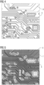
- Figure 4 shows a section of a printed circuit board without a mesh 7.
- Figure 5 shows the same section of the printed circuit board but having a mesh 7 of holes according to an embodiment of the invention.
- the holes in the mesh are quadratic and arranged equidistantly and in rows.
- Several electronic signal lines are running across the mesh.
- the size of the holes, i.e. the side length of the quadrats may preferably be in the range of 100 to 250 micrometres.
- Figure 6 shows a section of a printed circuit board comprising a slit 9 that is cutting at least partially through the conducting layer.
- this section or a similar section having a slit 9 may be combined with a section having the mesh 7.
- the slit may also be running across a mesh 7.
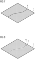
- Figure 7 shows an electronic signal line 8 running across a mesh 7 of a circuit board according to an embodiment of the invention.
- Figure 8 shows a similar signal line 8 running across a mesh 7 of a circuit board according to an embodiment of the invention.
- the circuit board comprises a trace of conducting material running across the mesh and following the course of the at least one signal line.
- the trace 10 of conducting material is wider than the signal line 8, such that, across the mesh, the signal line 8 is widened by the trace 10 of conducting material.
- the signal line may, for example, be a signal line for a clock signal.
Landscapes
- Health & Medical Sciences (AREA)
- Life Sciences & Earth Sciences (AREA)
- Engineering & Computer Science (AREA)
- Nuclear Medicine, Radiotherapy & Molecular Imaging (AREA)
- Medical Informatics (AREA)
- Physics & Mathematics (AREA)
- Biophysics (AREA)
- Animal Behavior & Ethology (AREA)
- Biomedical Technology (AREA)
- Heart & Thoracic Surgery (AREA)
- Radiology & Medical Imaging (AREA)
- Molecular Biology (AREA)
- Surgery (AREA)
- Pathology (AREA)
- General Health & Medical Sciences (AREA)
- Public Health (AREA)
- Veterinary Medicine (AREA)
- High Energy & Nuclear Physics (AREA)
- Optics & Photonics (AREA)
- Computer Networks & Wireless Communication (AREA)
- Structure Of Printed Boards (AREA)
- Magnetic Resonance Imaging Apparatus (AREA)
Priority Applications (2)
| Application Number | Priority Date | Filing Date | Title |
|---|---|---|---|
| EP23191117.3A EP4505943A1 (fr) | 2023-08-11 | 2023-08-11 | Carte de circuit imprimé pour un système d'imagerie |
| PCT/EP2024/067205 WO2025036596A1 (fr) | 2023-08-11 | 2024-06-20 | Carte de circuit imprimé pour système d'imagerie |
Applications Claiming Priority (1)
| Application Number | Priority Date | Filing Date | Title |
|---|---|---|---|
| EP23191117.3A EP4505943A1 (fr) | 2023-08-11 | 2023-08-11 | Carte de circuit imprimé pour un système d'imagerie |
Publications (1)
| Publication Number | Publication Date |
|---|---|
| EP4505943A1 true EP4505943A1 (fr) | 2025-02-12 |
Family
ID=87570885
Family Applications (1)
| Application Number | Title | Priority Date | Filing Date |
|---|---|---|---|
| EP23191117.3A Pending EP4505943A1 (fr) | 2023-08-11 | 2023-08-11 | Carte de circuit imprimé pour un système d'imagerie |
Country Status (2)
| Country | Link |
|---|---|
| EP (1) | EP4505943A1 (fr) |
| WO (1) | WO2025036596A1 (fr) |
Citations (3)
| Publication number | Priority date | Publication date | Assignee | Title |
|---|---|---|---|---|
| US20120206139A1 (en) * | 2007-01-11 | 2012-08-16 | Koninklijke Philips Electronics N. V. | Pet/mr scanners for simultaneous pet and mr imaging |
| US20120242339A1 (en) * | 2009-12-10 | 2012-09-27 | Koninklijke Philips Electronics N.V. | Magnetic resonance-compatible electrical device with radio frequency shielding or an enclosure |
| US20220099769A1 (en) * | 2019-06-14 | 2022-03-31 | Bruker Biospin Mri Gmbh | Imaging device, method for designing a circuit board arrangement, and circuit board arrangement |
-
2023
- 2023-08-11 EP EP23191117.3A patent/EP4505943A1/fr active Pending
-
2024
- 2024-06-20 WO PCT/EP2024/067205 patent/WO2025036596A1/fr active Pending
Patent Citations (3)
| Publication number | Priority date | Publication date | Assignee | Title |
|---|---|---|---|---|
| US20120206139A1 (en) * | 2007-01-11 | 2012-08-16 | Koninklijke Philips Electronics N. V. | Pet/mr scanners for simultaneous pet and mr imaging |
| US20120242339A1 (en) * | 2009-12-10 | 2012-09-27 | Koninklijke Philips Electronics N.V. | Magnetic resonance-compatible electrical device with radio frequency shielding or an enclosure |
| US20220099769A1 (en) * | 2019-06-14 | 2022-03-31 | Bruker Biospin Mri Gmbh | Imaging device, method for designing a circuit board arrangement, and circuit board arrangement |
Also Published As
| Publication number | Publication date |
|---|---|
| WO2025036596A1 (fr) | 2025-02-20 |
Similar Documents
| Publication | Publication Date | Title |
|---|---|---|
| US6163240A (en) | Magnetic apparatus for MRI | |
| JP6069129B2 (ja) | 平面的rfセンサ技術の強化について | |
| Lee et al. | Low eddy current RF shielding enclosure designs for 3T MR applications | |
| US8379403B2 (en) | Spacer-connector and circuit board assembly | |
| CN102652027B (zh) | 具有射频屏蔽或外罩的磁共振兼容电子装置 | |
| EP2895874B1 (fr) | Isoler des sondes de champ magnétique rm à partir de rayonnement rf externe | |
| EP4220213A2 (fr) | Bobine à radiofréquence de type cage d'oiseau destiné à une radiothérapie guidée par irm | |
| EP3490346B1 (fr) | Trace différentielle à grande vitesse avec rayonnement réduit lors du trajet de retour | |
| EP4505943A1 (fr) | Carte de circuit imprimé pour un système d'imagerie | |
| US9612305B2 (en) | Shielding for an electronic circuit | |
| US6798204B2 (en) | Local RF MRI coil using metal foil construction on a double-sided substrate with holes that directly pass DC conductors | |
| US7501583B2 (en) | Low noise multilayer printed circuit board | |
| US20130088233A1 (en) | Shield for Electronic Circuit | |
| CN109223019A (zh) | 一种pet探测单元及pet探测器 | |
| US20100109667A1 (en) | Transverse electromagnetic radio-frequency coil | |
| CN109085520A (zh) | 磁共振屏蔽单元 | |
| US20240192296A1 (en) | Self-tuning liquid metal rf coil and coil array for mri | |
| EP2175289A1 (fr) | Composant à résonance magnétique nucléaire comportant un blindage électromagnétique | |
| EP0430104A2 (fr) | Appareil d'imagerie par résonance magnétique | |
| US7239141B2 (en) | Magnetic resonance apparatus and gradient coil/radio frequency unit therefor with fracture-resistant electrical connections | |
| DE102011086285B4 (de) | Lokalspule | |
| CN113875319B (zh) | 成像设备、用于设计电路板装置的方法和电路板装置 | |
| JP3866960B2 (ja) | 磁気共鳴撮像装置 | |
| EP2733499A1 (fr) | Agencement de bobine IRM et procédé de fabrication de celui-ci | |
| KR102872772B1 (ko) | 자기공명영상용 rf 스트립 조립체 |
Legal Events
| Date | Code | Title | Description |
|---|---|---|---|
| PUAI | Public reference made under article 153(3) epc to a published international application that has entered the european phase |
Free format text: ORIGINAL CODE: 0009012 |
|
| STAA | Information on the status of an ep patent application or granted ep patent |
Free format text: STATUS: THE APPLICATION HAS BEEN PUBLISHED |
|
| AK | Designated contracting states |
Kind code of ref document: A1 Designated state(s): AL AT BE BG CH CY CZ DE DK EE ES FI FR GB GR HR HU IE IS IT LI LT LU LV MC ME MK MT NL NO PL PT RO RS SE SI SK SM TR |
|
| STAA | Information on the status of an ep patent application or granted ep patent |
Free format text: STATUS: REQUEST FOR EXAMINATION WAS MADE |
|
| 17P | Request for examination filed |
Effective date: 20250620 |
|
| STAA | Information on the status of an ep patent application or granted ep patent |
Free format text: STATUS: EXAMINATION IS IN PROGRESS |
|
| 17Q | First examination report despatched |
Effective date: 20251107 |