EP4507009A9 - Dispositif semi-conducteur - Google Patents
Dispositif semi-conducteur Download PDFInfo
- Publication number
- EP4507009A9 EP4507009A9 EP24155656.2A EP24155656A EP4507009A9 EP 4507009 A9 EP4507009 A9 EP 4507009A9 EP 24155656 A EP24155656 A EP 24155656A EP 4507009 A9 EP4507009 A9 EP 4507009A9
- Authority
- EP
- European Patent Office
- Prior art keywords
- partial region
- electrode
- region
- semiconductor
- insulating
- Prior art date
- Legal status (The legal status is an assumption and is not a legal conclusion. Google has not performed a legal analysis and makes no representation as to the accuracy of the status listed.)
- Pending
Links
Images


Classifications
-
- H—ELECTRICITY
- H10—SEMICONDUCTOR DEVICES; ELECTRIC SOLID-STATE DEVICES NOT OTHERWISE PROVIDED FOR
- H10D—INORGANIC ELECTRIC SEMICONDUCTOR DEVICES
- H10D30/00—Field-effect transistors [FET]
- H10D30/40—FETs having zero-dimensional [0D], one-dimensional [1D] or two-dimensional [2D] charge carrier gas channels
- H10D30/47—FETs having zero-dimensional [0D], one-dimensional [1D] or two-dimensional [2D] charge carrier gas channels having two-dimensional [2D] charge carrier gas channels, e.g. nanoribbon FETs or high electron mobility transistors [HEMT]
- H10D30/471—High electron mobility transistors [HEMT] or high hole mobility transistors [HHMT]
- H10D30/475—High electron mobility transistors [HEMT] or high hole mobility transistors [HHMT] having wider bandgap layer formed on top of lower bandgap active layer, e.g. undoped barrier HEMTs such as i-AlGaN/GaN HEMTs
-
- H—ELECTRICITY
- H10—SEMICONDUCTOR DEVICES; ELECTRIC SOLID-STATE DEVICES NOT OTHERWISE PROVIDED FOR
- H10D—INORGANIC ELECTRIC SEMICONDUCTOR DEVICES
- H10D30/00—Field-effect transistors [FET]
- H10D30/40—FETs having zero-dimensional [0D], one-dimensional [1D] or two-dimensional [2D] charge carrier gas channels
- H10D30/47—FETs having zero-dimensional [0D], one-dimensional [1D] or two-dimensional [2D] charge carrier gas channels having two-dimensional [2D] charge carrier gas channels, e.g. nanoribbon FETs or high electron mobility transistors [HEMT]
- H10D30/471—High electron mobility transistors [HEMT] or high hole mobility transistors [HHMT]
- H10D30/476—High electron mobility transistors [HEMT] or high hole mobility transistors [HHMT] having gate trenches interrupting the 2D charge carrier gas channels, e.g. hybrid MOS-HEMTs
-
- H—ELECTRICITY
- H10—SEMICONDUCTOR DEVICES; ELECTRIC SOLID-STATE DEVICES NOT OTHERWISE PROVIDED FOR
- H10D—INORGANIC ELECTRIC SEMICONDUCTOR DEVICES
- H10D62/00—Semiconductor bodies, or regions thereof, of devices having potential barriers
- H10D62/10—Shapes, relative sizes or dispositions of the regions of the semiconductor bodies; Shapes of the semiconductor bodies
- H10D62/113—Isolations within a component, i.e. internal isolations
- H10D62/115—Dielectric isolations, e.g. air gaps
-
- H—ELECTRICITY
- H10—SEMICONDUCTOR DEVICES; ELECTRIC SOLID-STATE DEVICES NOT OTHERWISE PROVIDED FOR
- H10D—INORGANIC ELECTRIC SEMICONDUCTOR DEVICES
- H10D62/00—Semiconductor bodies, or regions thereof, of devices having potential barriers
- H10D62/80—Semiconductor bodies, or regions thereof, of devices having potential barriers characterised by the materials
- H10D62/85—Semiconductor bodies, or regions thereof, of devices having potential barriers characterised by the materials being Group III-V materials, e.g. GaAs
- H10D62/8503—Nitride Group III-V materials, e.g. AlN or GaN
-
- H—ELECTRICITY
- H10—SEMICONDUCTOR DEVICES; ELECTRIC SOLID-STATE DEVICES NOT OTHERWISE PROVIDED FOR
- H10D—INORGANIC ELECTRIC SEMICONDUCTOR DEVICES
- H10D64/00—Electrodes of devices having potential barriers
- H10D64/20—Electrodes characterised by their shapes, relative sizes or dispositions
- H10D64/27—Electrodes not carrying the current to be rectified, amplified, oscillated or switched, e.g. gates
- H10D64/311—Gate electrodes for field-effect devices
- H10D64/411—Gate electrodes for field-effect devices for FETs
- H10D64/511—Gate electrodes for field-effect devices for FETs for IGFETs
- H10D64/512—Disposition of the gate electrodes, e.g. buried gates
- H10D64/513—Disposition of the gate electrodes, e.g. buried gates within recesses in the substrate, e.g. trench gates, groove gates or buried gates
-
- H—ELECTRICITY
- H10—SEMICONDUCTOR DEVICES; ELECTRIC SOLID-STATE DEVICES NOT OTHERWISE PROVIDED FOR
- H10D—INORGANIC ELECTRIC SEMICONDUCTOR DEVICES
- H10D64/00—Electrodes of devices having potential barriers
- H10D64/20—Electrodes characterised by their shapes, relative sizes or dispositions
- H10D64/23—Electrodes carrying the current to be rectified, amplified, oscillated or switched, e.g. sources, drains, anodes or cathodes
- H10D64/251—Source or drain electrodes for field-effect devices
- H10D64/257—Source or drain electrodes for field-effect devices for lateral devices wherein the source or drain electrodes are characterised by top-view geometrical layouts, e.g. interdigitated, semi-circular, annular or L-shaped electrodes
-
- H—ELECTRICITY
- H10—SEMICONDUCTOR DEVICES; ELECTRIC SOLID-STATE DEVICES NOT OTHERWISE PROVIDED FOR
- H10D—INORGANIC ELECTRIC SEMICONDUCTOR DEVICES
- H10D64/00—Electrodes of devices having potential barriers
- H10D64/20—Electrodes characterised by their shapes, relative sizes or dispositions
- H10D64/27—Electrodes not carrying the current to be rectified, amplified, oscillated or switched, e.g. gates
- H10D64/311—Gate electrodes for field-effect devices
- H10D64/411—Gate electrodes for field-effect devices for FETs
- H10D64/511—Gate electrodes for field-effect devices for FETs for IGFETs
- H10D64/517—Gate electrodes for field-effect devices for FETs for IGFETs characterised by the conducting layers
- H10D64/518—Gate electrodes for field-effect devices for FETs for IGFETs characterised by the conducting layers characterised by their lengths or sectional shapes
Definitions
- Embodiments described herein generally relate to a semiconductor device.
- semiconductor devices such as transistors are desired to have improved characteristics.
- a semiconductor device includes a first electrode, a second electrode, a third electrode, a first semiconductor member, a second semiconductor member, a first insulating member, and a second insulating member.
- the first electrode extends along a first direction.
- the second electrode extends along the first direction.
- a second direction from the first electrode to the second electrode crosses the first direction.
- the third electrode extends along the first direction.
- a position of the third electrode in the second direction is between a position of the first electrode in the second direction and a position of the second electrode in the second direction.
- the third electrode includes a first electrode portion.
- the first semiconductor member includes Al x1 Ga 1-x1 N(0 ⁇ x1 ⁇ 1).
- the first semiconductor member includes a first partial region, a second partial region, a third partial region, a fourth partial region, a fifth partial region, and a sixth partial region.
- a direction from the first partial region to the first electrode is along a third direction crossing a plane including the first direction and the second direction.
- a direction from the second partial region to the second electrode is along the third direction.
- a direction from the third partial region to the first electrode portion is along the third direction.
- a position of the fourth partial region in the second direction is between a position of the first partial region in the second direction and a position of the third partial region in the second direction.
- a position of the fifth partial region in the second direction is between the position of the third partial region in the second direction and a position of the second partial region in the second direction.
- a direction from the third partial region to the sixth partial region is along the first direction.
- the second semiconductor member includes Al x2 Ga 1-x2 N (0 ⁇ x2 ⁇ 1, x1 ⁇ x2).
- the second semiconductor member includes a first semiconductor portion, a second semiconductor portion and a third semiconductor portion.
- a direction from the fourth partial region to the first semiconductor portion is along the third direction.
- a direction from the fifth partial region to the second semiconductor portion is along the third direction.
- a direction from the sixth partial region to the third semiconductor portion is along the third direction.
- the first electrode portion is provided between the first semiconductor portion and the second semiconductor portion in the second direction.
- a direction from the first electrode portion to the third semiconductor portion is along the first direction.
- the first insulating member includes a first insulating portion.
- the first insulating portion is provided between the third partial region and the first electrode portion, between the first semiconductor portion and the first electrode portion, and between the first electrode portion and the second semiconductor portion.
- the second insulating member includes a first insulating region. The first insulating region is provided between the third electrode and the third semiconductor portion in the first direction.
- a semiconductor device 110 includes a first electrode 51, a second electrode 52, a third electrode 53, a first semiconductor member 10, a second semiconductor member 20, and a first insulating member 41 , and a second insulating member 42.
- the first electrode 51, the second electrode 52 and the third electrode 53 extend along a first direction D1.
- the first direction D1 is defines as a Y-axis direction.
- One direction perpendicular to the Y-axis direction is defined as an X-axis direction.
- a direction perpendicular to the Y-axis direction and the X-axis direction is defined as a Z-axis direction.
- the length in the Y-axis direction is longer than the length in the X-axis direction and longer than the length in the Z-axis direction.
- the second direction D2 is, for example, the X-axis direction.
- a position of the third electrode 53 in the second direction D2 is between a position of the first electrode 51 in the second direction D2 and a position of the second electrode 52 in the second direction D2.
- the third electrode 53 includes a first electrode portion 53a.
- the first electrode portion 53a extends along the first direction D1.
- the first semiconductor member 10 includes Al x1 Ga 1-x1 N(0 ⁇ x1 ⁇ 1).
- the composition ratio x1 may be, for example, not less than 0 and less than 0.13.
- the first semiconductor member 10 may be GaN or AlGaN.
- the first semiconductor member 10 includes a first partial region r1, a second partial region r2, a third partial region r3, a fourth partial region r4, a fifth partial region r5, and a sixth partial region r6.
- a direction from the first partial region r1 to the first electrode 51 is along a third direction D3.
- the third direction D3 crosses a plane including the first direction D1 and the second direction D2.
- the third direction D3 is, for example, the Z-axis direction.
- a direction from the second partial region r2 to the second electrode 52 is along the third direction D3.
- a direction from the third partial region r3 to the first electrode portion 53a is along the third direction D3.
- a position of the fourth partial region r4 in the second direction D2 is between a position of the first partial region r1 in the second direction D2 and a position of the third partial region r3 in the second direction D2.
- a position of the fifth partial region r5 in the second direction D2 is between the position of the third partial region r3 in the second direction D2 and a position of the second partial region r2 in the second direction D2.
- a direction from the third partial region r3 to the sixth partial region r6 is along the first direction D1 (see FIG. 3 ).
- the second semiconductor member 20 includes Al x2 Ga 1-x2 N (0 ⁇ x2 ⁇ 1, x1 ⁇ x2).
- the composition ratio x2 may be, for example, not less than 0.13 and not more than 0.4.
- the second semiconductor member 20 includes, for example, AlGaN.
- the second semiconductor member 20 includes a first semiconductor portion 21 and a second semiconductor portion 22.
- a direction from the fourth partial region r4 to the first semiconductor portion 21 is along the third direction D3.
- a direction from the fifth partial region r5 to the second semiconductor portion 22 is along the third direction D3.
- the second semiconductor member 20 further includes a third semiconductor portion 23.
- a direction from the sixth partial region r6 to the third semiconductor portion 23 is along the third direction D3.
- the first electrode portion 53a is provided between the first semiconductor portion 21 and the second semiconductor portion 22 in the second direction D2.
- a direction from the first electrode portion 53a to the third semiconductor portion 23 is along the first direction D1.
- the first insulating member 41 includes a first insulating portion 41a. As shown in FIGS. 2 and 3 , the first insulating portion 41a is provided between the third partial region r3 and the first electrode portion 53a, between the first semiconductor portion 21 and the first electrode portion 53a, and between the first electrode portion 53a and the second semiconductor portion 22.
- the second insulating member 42 includes a first insulating region 42a.
- the first insulating region 42a is provided between the third electrode 53 and the third semiconductor portion 23 in the first direction D1.
- a current flowing between the first electrode 51 and the second electrode 52 can be controlled by a potential of the third electrode 53.
- the potential of the third electrode 53 may be based on a potential of the first electrode 51.
- the first electrode 51 functions, for example, as a source electrode.
- the second electrode 52 functions, for example, as a drain electrode.
- the third electrode 53 functions as, for example, a gate electrode.
- the semiconductor device 110 is, for example, a transistor.
- a distance between the first electrode 51 and the third electrode 53 is shorter than a distance between the third electrode 53 and the second electrode 52. It is easy to obtain stable operation.
- the first electrode portion 53a of the third electrode 53 is provided between the first semiconductor portion 21 and the second semiconductor portion 22.
- the first electrode portion 53a is provided, for example, in a trench 53T (or recess) provided in the semiconductor member. This makes it easy to obtain a high threshold. For example, normally-off operation is obtained.
- the first electrode portion 53a may be provided between the fourth partial region r4 and the fifth partial region r5.
- the first insulating region 42a is provided between the third electrode 53 and the third semiconductor portion 23. Thereby, leakage current can be suppressed.
- a first reference example may be considered in which the first insulating region 42a is not provided.
- current easily flows between the first semiconductor portion 21 and the second semiconductor portion 22 via the third semiconductor portion 23. Leakage current occurs. This makes it difficult to sufficiently lower the off-resistance.
- leakage current can be suppressed.
- This provides, for example, normally-off operation with sufficiently low off-resistance.
- leakage current can be suppressed by not overlapping the third electrode 53 with the third semiconductor portion 23 in the Z-axis direction. This provides normally-off operation with sufficiently low off-resistance.
- a semiconductor device with improved characteristics can be provided.
- the semiconductor device 110 may include a first region R1, a second region R2 and a third region R3.
- the first region R1 is provided between the second region R2 and the third region R3 in the first direction D1.
- the first region R1 is an active region.
- the second region R2 is one of the plurality of terminal regions.
- the third region R3 is another one of the plurality of terminal regions.
- the first partial region r1, the second partial region r2, the third partial region r3, the fourth partial region r4, and the fifth partial region r5 are included in the first region R1.
- the sixth partial region r6 is included in the second region R2.
- a crystallinity of the first region R1 is higher than a crystallinity of the second region R2.
- the first region R1 includes crystal and the second region R2 does not include crystal.
- the second region R2 is formed, for example, by implanting ions such as Ar into the semiconductor member to deteriorate the crystallinity of the semiconductor member.
- the first region R1 is a region into which ions are not implanted.
- a concentration of the first element in the second region R2 is higher than a concentration of the first element in the first region R1.
- the first element includes at least one selected from the group consisting of Ar, P and N.
- a second reference example can be considered in which an end of the third electrode 53 is provided in the second region R2.
- a part of the second region R2 is covered with the third electrode 53. Ions are not implanted into the portion covered with the third electrode 53, and high crystallinity is maintained. This portion has high conductivity and serves as a path for leakage current.
- the crystallinity may be recovered by subsequent heat treatment. In this case as well, a leakage current path exists.
- the end of the third electrode 53 is located in the first region R1.
- the portion not covered by the third electrode 53 is not provided in the second region R2, which is the termination region.
- the end of the third electrode 53 recessed from the end of the trench 53T.
- a portion where the second semiconductor member 20 is not provided is formed in the second region R2 of the termination region.
- a carrier region is not formed in the second region R2.
- the first insulating region 42a is provided in a portion where the third electrode 53 is recessed. The current path is surely divided.
- the second region R2 includes a high resistance region 10i.
- the high resistance region 10i is a region into which ions such as Ar are implanted.
- the sixth partial region r6 and the third semiconductor portion 23 are included in the high resistance region 10i.
- the crystallinity in these regions included in the high resistance region 10i is lower than the crystallinity in the region (first region R1) not included in the high resistance region 10i.
- a crystallinity of the first semiconductor portion 21 is higher than a crystallinity of the third semiconductor portion 23.
- the first semiconductor portion 21 includes crystal, and the third semiconductor portion 23 does not include crystal.
- a crystallinity of the fourth partial region r4 is higher than a crystallinity of the sixth partial region r6.
- the fourth partial region r4 include crystal and the sixth partial region r6 does not include crystal.
- a crystallinity of the fifth partial region r5 is higher than the crystallinity of the sixth partial region r6.
- the fifth partial region r5 includes crystal and the sixth partial region r6 does not include crystal.
- the first semiconductor member 10 may further include a seventh partial region r7.
- the third partial region r3 is provided between the seventh partial region r7 and the sixth partial region r6 in the first direction D1.
- the second semiconductor member 20 may further include a fourth semiconductor portion 24.
- the first electrode portion 53a is provided between the fourth semiconductor portion 24 and the third semiconductor portion 23 in the first direction D1.
- the second insulating member 42 may further include a second insulating region 42b.
- the second insulating region 42b is provided between the fourth semiconductor portion 24 and the third electrode 53 in the first direction D1.
- the third region R3 is, for example, a region into which ions such as Ar are implanted.
- the seventh partial region r7 and the fourth semiconductor portion 24 are included in the third region R3.
- the crystallinity of the seventh partial region r7 and the fourth semiconductor portion 24 included in the third region R3 is lower than the crystallinity of the portion included in the first region R1.
- the third region R3 includes the high resistance region 10i.
- the high resistance region 10i is a region into which ions such as Ar are implanted.
- the seventh partial region r7 and the fourth semiconductor portion 24 are included in the high resistance region 10i.
- the crystallinity in these regions included in the high resistance region 10i is lower than the crystallinity in the region (first region R1) not included in the high resistance region 10i.
- the crystallinity of the first semiconductor portion 21 is higher than a crystallinity of the fourth semiconductor portion 24.
- the first semiconductor portion 21 includes crystal
- the fourth semiconductor portion 24 does not include crystal.
- the crystallinity of the fourth partial region r4 is higher than the crystallinity of the seventh partial region r7.
- the fourth partial region r4 includes crystal, and the seventh partial region r7 does not include crystal.
- the crystallinity of the fifth partial region r5 is higher than the crystallinity of the seventh partial region r7.
- the fifth partial region r5 includes crystal, and the seventh partial region r7 does not include crystal.
- the crystallinity of the first region R1 is higher than the crystallinity of the third region R3.
- the first region R1 includes crystal and the third region R3 does not include crystal.
- the third electrode 53 does not overlap the second region R2 in the third direction D3, and does not overlap the third region R3 in the third direction D3.
- the second electrode 52 does not overlap the second region R2 in the third direction D3, and does not overlap the third region R3 in the third direction D3.
- the first electrode 51 does not overlap the second region R2 in the third direction D3, and does not overlap the third region R3 in the third direction D3.
- the semiconductor device 110 may further include a first compound member 31.
- the first compound member 31 includes Al z1 Ga 1-z1 N (0 ⁇ z1 ⁇ 1, x2 ⁇ z1).
- the composition ratio z1 may be, for example, not more than 0.7 and not more than 1.
- the first compound member 31 includes, for example, AlN or AlGaN.
- At least a part of the first compound member 31 is provided between the third partial region r3 and the first insulating portion 41a, between the first semiconductor portion 21 and the first insulating portion 41a, and between the first insulating portion 41a and the second semiconductor portion 22.
- the first compound member 31 for example, high mobility is easily obtained.
- the resistance of the semiconductor device 110 can be lowered.
- the first insulating region 42a is not provided, when the first compound member 31 is provided, the current leakage tends to increase. By providing the first insulating region 42a, the current leakage can be effectively reduced even when the first compound member 31 is provided. High mobility and small leakage current are easily obtained.
- the semiconductor device 110 may further include a third insulating member 43.
- the first semiconductor portion 21 is provided between the fourth partial region r4 and a part of the third insulating member 43.
- the second semiconductor portion 22 is provided between the fifth partial region r5 and a part of the third insulating member 43.
- the third semiconductor portion 23 is provided between the sixth partial region r6 and a part of the third insulating member 43.
- the fourth semiconductor portion 24 is provided between the seventh partial region r7 and a part of the third insulating member 43.
- the third insulating member 43 is provided between the second semiconductor member 20 and the first insulating member 41.
- the third insulating member 43 includes, for example, silicon and at least one selected from the group consisting of oxygen and nitrogen.
- the third insulating member 43 functions as a protective film of the second semiconductor member 20, for example. Current collapse is suppressed.
- the first insulating member 41 and the second insulating member 42 may include silicon and oxygen.
- the first insulating member 41 and the second insulating member 42 may include, for example, at least one selected from the group consisting of silicon and aluminum, and at least one selected from the group consisting of oxygen and nitrogen.
- the first semiconductor portion 21 includes a first side face 21f facing the first electrode portion 53a.
- the second semiconductor portion 22 includes a second side face 22f facing the first electrode portion 53a.
- the first side face 21f and the second side face 22f correspond to the side faces of the trench 53T.
- the third electrode 53 may include a second electrode portion 53b.
- the first electrode portion 53a is provided between the third partial region r3 and the second electrode portion 53b.
- a length of the second electrode portion 53b in the second direction D2 (second electrode portion length L53b) may be longer than a first distance d1 in the second direction D2 between the first side face 21f and the second side face 22f.
- a part of the first insulating member 41 may be provided between a part of the second semiconductor member 20 and the second electrode portion 53b.
- the planar shape of the first insulating region 42a and the second insulating region 42b may be along the planar shape of the trench 53T.
- a first width L1 of the first insulating region 42a along the second direction D2 may be substantially the same as the first distance d1.
- a second width L2 of the second insulating region 42b along the second direction D2 may be substantially the same as the first distance d1.
- the first width L1 is shorter than the second electrode portion length L53b.
- the second width L2 is shorter than the second electrode portion length L53b.
- a depth z53 (see FIG. 2 ) of the trench 53T may be, for example, not less than 100 nm and not more than 400 nm.
- the depth z53 of the trench 53T corresponds to a distance along the third direction D3 between the interface between the third partial region r3 and the first compound member 31 and the interface between the second semiconductor member 20 and the third insulating member 43.
- the depth z53 of the trench 53T is 100 nm or more, the current leakage can be effectively suppressed. It is easy to obtain a high threshold voltage.
- the depth z53 of the trench 53T is 400 nm or less, the on-resistance of the semiconductor device 110 is easily lowered.
- the distance along the third direction D3 between the third partial region r3 and the first electrode portion 53a is, for example, not less than 20 nm and not more than 150 nm. Highly stable operation can be obtained. When the distance is 20 nm or more, it is easy to obtain stable operation with a threshold voltage, for example. When the distance is 150 nm or less, it is easy to obtain low on-resistance, for example.
- the semiconductor device 110 includes a substrate 10S and a nitride member 10B.
- the nitride member 10B is provided between the substrate 10S and the first semiconductor member 10.
- the substrate 10S may be, for example, a silicon substrate.
- the nitride member 10B may include, for example, Al, Ga, and nitrogen.
- the nitride member 10B is, for example, a buffer layer.
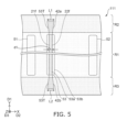
- FIG. 5 is a schematic plan view illustrating a semiconductor device according to the first embodiment.
- the shapes of the first insulating region 42a and the second insulating region 42b are different from those in the semiconductor device 110.
- the configuration of the semiconductor device 111 other than this may be the same as the configuration of the semiconductor device 110.
- the planar shapes of the first insulating region 42a and the second insulating region 42b may be trapezoids, for example. These planar shapes may be rectangular, for example.
- the first semiconductor portion 21 includes the first side face 21f facing the first electrode portion 53a.
- the second semiconductor portion 22 includes the second side face 22f facing the first electrode portion 53a.
- the distance along the second direction D2 between the first side face 21f and the second side face 22f is the first distance d1.
- the first distance d1 is narrower than the first width L1 along the second direction D2 of at least a part of the first insulating region 42a.
- the first distance d1 is narrower than the second width L2 in the second direction D2 of at least a part of the second insulating region 42b.
- Each of the first width L1 and the second width L2 is preferably not less than 1.5 times and not more than 10 times the first distance d1.
- FIG. 6 is a schematic plan view illustrating a semiconductor device according to the first embodiment.
- a plurality of third electrodes 53 are provided in a semiconductor device 112 in a semiconductor device 112. Except for this, the configuration of the semiconductor device 112 may be the same as the configuration of the semiconductor device 110.
- a plurality of first insulating regions 42a are provided corresponding to the plurality of third electrodes 53.
- a direction from one of the plurality of third electrodes 53 to one of the plurality of first insulating regions 42a is along the first direction D1.
- a direction from another one of the plurality of third electrodes 53 to another one of the plurality of first insulating regions 42a is along the first direction D1.
- a first plane PL1 including the first direction D1 and the second direction D2 one of the plurality of first insulating regions 42a is continuous with another one of the plurality of first insulating regions 42a.
- the current path between the first electrode 51 and the second electrode 52 is more surely divided.
- FIG. 7 is a schematic plan view illustrating a semiconductor device according to a second embodiment.
- FIGS. 8 to 13 are schematic cross-sectional views illustrating the semiconductor device according to the second embodiment.
- FIG. 8 is a cross-sectional view taken along the line A1-A2 of FIG. 7 .
- FIG. 9 is a sectional view taken along the line A3-A4 in FIG. 7 .
- FIG. 10 is a sectional view taken along the line A5-A6 in FIG.7 .
- FIG. 11 is a sectional view taken along the line B1-B2 in FIG. 7 .
- FIG. 12 is a sectional view taken along the line B3-B4 in FIG. 7 .
- FIG. 13 is a sectional view taken along the line B5-B6 in FIG. 7 .
- a semiconductor device 120 includes the first electrode 51, the second electrode 52, the third electrode 53, the first semiconductor member 10, the second semiconductor member 20, and the first insulating member. 41 and the second insulating member 42.
- the first electrode 51, the second electrode 52, and the third electrode 53 extend along the first direction D1.
- the second direction D2 from the first electrode 51 to the second electrode 52 crosses the first direction D1.
- the position of the third electrode 53 in the second direction D2 is between the position of the first electrode 51 in the second direction D2 and the position of the second electrode 52 in the second direction D2.
- the third electrode 53 includes the first electrode portion 53a.
- the first semiconductor member 10 includes Al x1 Ga 1-x1 N(0 ⁇ x1 ⁇ 1).
- the first semiconductor member 10 includes the first partial region r1, the second partial region r2, the third partial region r3, the fourth partial region r4, the fifth partial region r5, the sixth partial region r6 and the seventh partial region r7.
- the direction from the first partial region r1 to the first electrode 51 is along the third direction D3 that crosses the plane including the first direction D1 and the second direction D2.
- the direction from the second partial region r2 to the second electrode 52 is along the third direction D3.
- the direction from the third partial region r3 to the first electrode portion 53a is along the third direction D3.
- the position of the fourth partial region r4 in the second direction D2 is between the position of the first partial region r1 in the second direction D2 and the position of the third partial region r3 in the second direction D2.
- the position of the fifth partial region r5 in the second direction D2 is between the position of the third partial region r3 in the second direction D2 and the position of the second partial region r2 in the second direction D2.
- the direction from the third partial region r3 to the sixth partial region r6 is along the first direction D1.
- the direction from the seventh partial region r7 to the sixth partial region r6 is along the second direction D2.
- the second semiconductor member 20 includes Al x2 Ga 1-x2 N (0 ⁇ x2 ⁇ 1, x1 ⁇ x2).
- the second semiconductor member 20 includes the first semiconductor portion 21, the second semiconductor portion 22, and the third semiconductor portion 23.
- the direction from the fourth partial region r4 to the first semiconductor portion 21 is along the third direction D3.
- the direction from the fifth partial region r5 to the second semiconductor portion 22 is along the third direction D3.
- the direction from the seventh partial region r7 to the third semiconductor portion 23 is along the third direction D3.
- the first electrode portion 53a is provided between the first semiconductor portion 21 and the second semiconductor portion 22 in the second direction D2.
- the crystallinity of the first semiconductor portion 21 is higher than the crystallinity of the third semiconductor portion 23.
- the first semiconductor portion 21 includes crystal, and the third semiconductor portion 23 does not include crystal.
- the seventh partial region r7 and the third semiconductor portion 23 are included in the high resistance region 10i.
- the seventh partial region r7 and the third semiconductor portion 23 are included in the second region R2 (see FIG. 7 ).
- the first insulating member 41 includes the first insulating portion 41a.
- the first insulating portion 41a is provided between the third partial region r3 and the first electrode portion 53a, between the first semiconductor portion 21 and the first electrode portion 53a, and between the first electrode portion 53a and the second semiconductor portion 22.
- the second insulating member 42 includes the first insulating region 42a.
- the first insulating region 42a is provided between the third semiconductor portion 23 and the third electrode 53 in the second direction D2.
- the current path is divided by the first insulating region 42a. Leakage current is suppressed.
- a semiconductor device whose characteristics can be improved can be provided.
- the first semiconductor member 10 may further include an eighth partial region r8.
- the sixth partial region r6 is provided between the seventh partial region r7 and the eighth partial region r8 in the second direction D2.
- the second semiconductor member 20 may further include the fourth semiconductor portion 24. A direction from the eighth partial region r8 to the fourth semiconductor portion 24 is along the third direction D3.
- At least a part of the eighth partial region r8 and the fourth semiconductor portion 24 are included in the high resistance region 10i. At least a part of the eighth partial region r8 and the fourth semiconductor portion 24 are included in the second region R2.
- the crystallinity of the second semiconductor portion 22 is higher than the crystallinity of the fourth semiconductor portion 24.
- the second semiconductor portion 22 includes crystal, and the fourth semiconductor portion 24 does not include crystal.
- the second insulating member 42 further includes the second insulating region 42b.
- the second insulating region 42b is provided between the third electrode 53 and the fourth semiconductor portion 24 in the second direction D2.
- the current path is more reliably divided by the second insulating region 42b. Leakage current is suppressed.
- the first semiconductor member 10 may further include a ninth partial region r9. As shown in FIG. 11 , the third partial region r3 is provided between the ninth partial region r9 and the sixth partial region r6 in the first direction D1.
- the first semiconductor member 10 may further include a tenth partial region r10.
- a direction from the tenth partial region r10 to the ninth partial region r9 is along the second direction D2.
- the second semiconductor member 20 may further include a fifth semiconductor portion 25.
- a direction from the tenth partial region r10 to the fifth semiconductor portion 25 is along the third direction D3.
- the second insulating member 42 may include a third insulating region 42c.
- the third insulating region 42c is provided between the fifth semiconductor portion 25 and the third electrode 53 in the second direction D2.
- the current path is more surely divided by the third insulating region 42c. Leakage current is suppressed.
- the first semiconductor member 10 may further include an eleventh partial region r11.
- the ninth partial region r9 is provided between the tenth partial region r10 and the eleventh partial region r11.
- the second semiconductor member 20 may further include a sixth semiconductor portion 26. A direction from the eleventh partial region r11 to the sixth semiconductor portion 26 is along the third direction D3.
- the second insulating member 42 may include a fourth insulating region 42d.
- the fourth insulating region 42d is provided between the third electrode 53 and the sixth semiconductor portion 26 in the second direction D2.
- the current path is more reliably divided by the fourth insulating region 42d. Leakage current is suppressed.
- At least a part of the tenth partial region r10 and the fifth semiconductor portion 25 are included in the high resistance region 10i. At least a part of the tenth partial region r10 and the fifth semiconductor portion 25 are included in the third region R3.
- At least a part of the eleventh partial region r11 and the sixth semiconductor portion 26 are included in the high resistance region 10i. At least a part of the eleventh partial region r11 and the sixth semiconductor portion 26 are included in the third region R3.
- the crystallinity of the first semiconductor portion 21 is higher than the crystallinity of the fifth semiconductor portion 25.
- the first semiconductor portion 21 includes crystal, and the fifth semiconductor portion 25 does not include crystal.
- the crystallinity of the second semiconductor portion 22 is higher than the crystallinity of the sixth semiconductor portion 26.
- the second semiconductor portion 22 includes crystals and the sixth semiconductor portion 26 does not include crystal.
- the semiconductor device 120 may include the first compound member 31 .
- the first compound member 31 includes Al z1 Ga 1-z1 N (0 ⁇ z1 ⁇ 1, x2 ⁇ z1). At least a part of the first compound member 31 is provided between the third partial region r3 and the first insulating portion 41a, between the first semiconductor portion 21 and the first insulating portion 41a, and between the first insulating portion 41a and the second semiconductor portion 22.
- the first compound member 31 for example, high mobility is easily obtained. The resistance of the semiconductor device 120 can be lowered.
- FIG. 14 is a schematic plan view illustrating a semiconductor device according to the second embodiment.
- the third electrode 53 includes a third electrode portion 53c. Except for this, the configuration of the semiconductor device 121 may be the same as the configuration of the semiconductor device 120.
- the third electrode 53 includes the second electrode portion 53b and the third electrode portion 53c. As shown in FIG. 8 , the first electrode portion 53a is provided between the third partial region r3 and the second electrode portion 53b in the third direction D3.
- the position of the first insulating region 42a in the first direction D1 is between the position of the first electrode portion 53a in the first direction D1 and the position of the third electrode portion 53c in the first direction D1.
- a length of the third electrode portion 53c in the second direction D2 is defined as a third electrode portion length L53c.
- a length of the second electrode portion 53b in the second direction D2 is defined as the second electrode portion length L53b.
- the third electrode portion length L53c is longer than the second electrode portion length L53b.
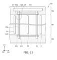
- FIG. 15 is a schematic plan view illustrating a semiconductor device according to the second embodiment.
- a semiconductor device 122 As shown in FIG. 15 , in a semiconductor device 122 according to the embodiment, a plurality of third electrodes 53 are provided. Except for this, the configuration of the semiconductor device 122 may be the same as the configuration of the semiconductor device 120.
- the second insulating region 42b is continuously provided between one of the plurality of third electrodes 53 and another one of the plurality of third electrodes 53.
- the first insulating region 42a and the second insulating region 42b may be interchanged.
- any one of the first insulating region 42a and the second insulating region 42b may be provided continuously between one of the plurality of third electrodes 53 and another one of the plurality of third electrodes 53.
- the semiconductor device 122 may further include a connecting conductive portion 53X.
- the connecting conductive portion 53X extends along the second direction D2.
- the position of the first insulating region 42a in the first direction D1 is between the position of the first electrode portion 53a in the first direction D1 and the position of the connecting conductive portion 53X in the first direction D1.
- the plurality of third electrodes 53 are provided.
- the connecting conductive portion 53X electrically connects one of the plurality of third electrodes 53 to another one of the plurality of third electrodes 53.
- FIG. 16 is a schematic plan view illustrating a semiconductor device according to an embodiment.
- a semiconductor device 130 includes a first electrode pad 51P, a second electrode pad 52P, and a third electrode pad 53P.
- the configuration of the semiconductor device 130 other than this may be the same as the configuration of any semiconductor device and its modification according to the first and second embodiments described above.
- a plurality of first electrodes 51, a plurality of second electrodes 52, and a plurality of third electrodes 53 are provided.
- the first electrode pad 51P is electrically connected to the plurality of first electrodes 51.
- the second electrode pad 52P is electrically connected to the plurality of second electrodes 52.
- the third electrode pad 53P is electrically connected to the plurality of third electrodes 53.
- the first electrode pad 51P and the third electrode pad 53P are provided in the third region R3.
- the second electrode pad 52P is provided in the second region R2.
- FIG. 17 is a schematic plan view illustrating a semiconductor device according to an embodiment.
- a semiconductor device 131 includes a first electrode connecting portion 51C and a third electrode connecting portion 53C.
- the configuration of the semiconductor device 131 other than this may be the same as the configuration of the semiconductor device 130.
- the first electrode connecting portion 51C and the third electrode connecting portion 53C extend along the second direction D2.
- the first electrode connecting portion 51C electrically connects the plurality of first electrodes 51.
- the third electrode connecting portion 53C electrically connects the plurality of third electrodes 53.
- the semiconductor device 130 and the semiconductor device 131 as well, at least the first insulating region 42a is provided. Leakage current can be suppressed. A semiconductor device whose characteristics can be improved can be provided.
- information regarding length and thickness is obtained, such as by electron microscopy.
- Information regarding the composition of the material can be obtained by SIMS (Secondary Ion Mass Spectrometry), EDX (Energy dispersive X-ray spectroscopy), or the like.
- Information regarding crystallinity can be obtained, such as by PL (Photo Luminescence).
- Embodiments may include following technical proposals.
- a semiconductor device comprising:
- the semiconductor device according to any one of Technical proposals 1-12, further comprising:
- the semiconductor device according to any one of Technical proposals 1-13, further comprising:
- a semiconductor device comprising:
- the semiconductor device according to Technical proposal 15 further comprising:
- a semiconductor device with improved characteristics can be provided.
Landscapes
- Insulated Gate Type Field-Effect Transistor (AREA)
- Electrodes Of Semiconductors (AREA)
- Junction Field-Effect Transistors (AREA)
Applications Claiming Priority (1)
| Application Number | Priority Date | Filing Date | Title |
|---|---|---|---|
| JP2023131140A JP2025025908A (ja) | 2023-08-10 | 2023-08-10 | 半導体装置 |
Publications (3)
| Publication Number | Publication Date |
|---|---|
| EP4507009A2 EP4507009A2 (fr) | 2025-02-12 |
| EP4507009A9 true EP4507009A9 (fr) | 2025-05-07 |
| EP4507009A3 EP4507009A3 (fr) | 2025-05-28 |
Family
ID=89843717
Family Applications (1)
| Application Number | Title | Priority Date | Filing Date |
|---|---|---|---|
| EP24155656.2A Pending EP4507009A3 (fr) | 2023-08-10 | 2024-02-20 | Dispositif semi-conducteur |
Country Status (4)
| Country | Link |
|---|---|
| US (1) | US20250056826A1 (fr) |
| EP (1) | EP4507009A3 (fr) |
| JP (1) | JP2025025908A (fr) |
| CN (1) | CN119521713A (fr) |
Family Cites Families (6)
| Publication number | Priority date | Publication date | Assignee | Title |
|---|---|---|---|---|
| JP2014135439A (ja) * | 2013-01-11 | 2014-07-24 | Renesas Electronics Corp | 半導体装置および半導体装置の製造方法 |
| JP7446727B2 (ja) * | 2019-07-04 | 2024-03-11 | 株式会社東芝 | 半導体装置 |
| US20220130986A1 (en) * | 2020-10-26 | 2022-04-28 | Kabushiki Kaisha Toshiba | Semiconductor device |
| US12513934B2 (en) * | 2020-10-26 | 2025-12-30 | Kabushiki Kaisha Toshiba | Semiconductor device |
| US12237409B2 (en) * | 2021-08-27 | 2025-02-25 | Kabushiki Kaisha Toshiba | Semiconductor device |
| JP7805321B2 (ja) * | 2023-01-17 | 2026-01-23 | 株式会社東芝 | 半導体装置 |
-
2023
- 2023-08-10 JP JP2023131140A patent/JP2025025908A/ja active Pending
-
2024
- 2024-02-01 US US18/429,925 patent/US20250056826A1/en active Pending
- 2024-02-20 EP EP24155656.2A patent/EP4507009A3/fr active Pending
- 2024-02-23 CN CN202410199811.2A patent/CN119521713A/zh active Pending
Also Published As
| Publication number | Publication date |
|---|---|
| EP4507009A3 (fr) | 2025-05-28 |
| JP2025025908A (ja) | 2025-02-21 |
| CN119521713A (zh) | 2025-02-25 |
| US20250056826A1 (en) | 2025-02-13 |
| EP4507009A2 (fr) | 2025-02-12 |
Similar Documents
| Publication | Publication Date | Title |
|---|---|---|
| US20160240614A1 (en) | Semiconductor device and semiconductor package | |
| CN102237402A (zh) | 氮化物半导体元件 | |
| US11715778B2 (en) | Semiconductor device | |
| US12119377B2 (en) | SiC devices with shielding structure | |
| US20220130986A1 (en) | Semiconductor device | |
| US11139395B2 (en) | Semiconductor device | |
| US20250374586A1 (en) | Semiconductor device | |
| US12237409B2 (en) | Semiconductor device | |
| EP4507009A9 (fr) | Dispositif semi-conducteur | |
| US20250212499A1 (en) | Semiconductor device | |
| JP5289818B2 (ja) | Iii族窒化物半導体装置とその製造方法 | |
| US20220384629A1 (en) | Semiconductor device | |
| EP4418329A1 (fr) | Dispositif semi-conducteur et son procédé de fabrication | |
| US12087823B2 (en) | Semiconductor device | |
| US20220140125A1 (en) | Semiconductor device | |
| US20250169148A1 (en) | Semiconductor device | |
| US11251293B2 (en) | Semiconductor device | |
| US20250203909A1 (en) | Semiconductor device | |
| US20250063752A1 (en) | Semiconductor device | |
| US20260096131A1 (en) | Semiconductor device | |
| US12550396B2 (en) | Semiconductor device | |
| US20250113524A1 (en) | Nitride structure and semiconductor device | |
| US20250261421A1 (en) | Wafer and semiconductor device | |
| US20250386579A1 (en) | Semiconductor device | |
| JP2025082236A (ja) | 半導体装置 |
Legal Events
| Date | Code | Title | Description |
|---|---|---|---|
| PUAI | Public reference made under article 153(3) epc to a published international application that has entered the european phase |
Free format text: ORIGINAL CODE: 0009012 |
|
| STAA | Information on the status of an ep patent application or granted ep patent |
Free format text: STATUS: REQUEST FOR EXAMINATION WAS MADE |
|
| 17P | Request for examination filed |
Effective date: 20240205 |
|
| AK | Designated contracting states |
Kind code of ref document: A2 Designated state(s): AL AT BE BG CH CY CZ DE DK EE ES FI FR GB GR HR HU IE IS IT LI LT LU LV MC ME MK MT NL NO PL PT RO RS SE SI SK SM TR |
|
| REG | Reference to a national code |
Ref country code: DE Ref legal event code: R079 Free format text: PREVIOUS MAIN CLASS: H01L0029778000 Ipc: H10D0030470000 |
|
| PUAL | Search report despatched |
Free format text: ORIGINAL CODE: 0009013 |
|
| XX | Miscellaneous (additional remarks) |
Free format text: APPLICATION REPUBLISHED WITH CORRECT DRAWINGS FILED UNDER RULE 56A(3) EPC |
|
| AK | Designated contracting states |
Kind code of ref document: A3 Designated state(s): AL AT BE BG CH CY CZ DE DK EE ES FI FR GB GR HR HU IE IS IT LI LT LU LV MC ME MK MT NL NO PL PT RO RS SE SI SK SM TR Free format text: APPLICATION REPUBLISHED WITH CORRECT DRAWINGS FILED UNDER RULE 56A(3) EPC |
|
| RIC1 | Information provided on ipc code assigned before grant |
Ipc: H10D 62/85 20250101ALN20250423BHEP Ipc: H10D 64/23 20250101ALN20250423BHEP Ipc: H10D 64/27 20250101ALI20250423BHEP Ipc: H10D 30/47 20250101AFI20250423BHEP |