EP4507183A1 - Systèmes et procédés pour condensateur de stabilisation à inductance de commutation inférieure - Google Patents
Systèmes et procédés pour condensateur de stabilisation à inductance de commutation inférieure Download PDFInfo
- Publication number
- EP4507183A1 EP4507183A1 EP24189131.6A EP24189131A EP4507183A1 EP 4507183 A1 EP4507183 A1 EP 4507183A1 EP 24189131 A EP24189131 A EP 24189131A EP 4507183 A1 EP4507183 A1 EP 4507183A1
- Authority
- EP
- European Patent Office
- Prior art keywords
- busbar
- capacitors
- stacked
- capacitor
- assembly
- Prior art date
- Legal status (The legal status is an assumption and is not a legal conclusion. Google has not performed a legal analysis and makes no representation as to the accuracy of the status listed.)
- Pending
Links
Images




Classifications
-
- H—ELECTRICITY
- H02—GENERATION; CONVERSION OR DISTRIBUTION OF ELECTRIC POWER
- H02M—APPARATUS FOR CONVERSION BETWEEN AC AND AC, BETWEEN AC AND DC, OR BETWEEN DC AND DC, AND FOR USE WITH MAINS OR SIMILAR POWER SUPPLY SYSTEMS; CONVERSION OF DC OR AC INPUT POWER INTO SURGE OUTPUT POWER; CONTROL OR REGULATION THEREOF
- H02M7/00—Conversion of AC power input into DC power output; Conversion of DC power input into AC power output
- H02M7/42—Conversion of DC power input into AC power output without possibility of reversal
- H02M7/44—Conversion of DC power input into AC power output without possibility of reversal by static converters
- H02M7/48—Conversion of DC power input into AC power output without possibility of reversal by static converters using discharge tubes with control electrode or semiconductor devices with control electrode
- H02M7/53—Conversion of DC power input into AC power output without possibility of reversal by static converters using discharge tubes with control electrode or semiconductor devices with control electrode using devices of a triode or transistor type requiring continuous application of a control signal
- H02M7/537—Conversion of DC power input into AC power output without possibility of reversal by static converters using discharge tubes with control electrode or semiconductor devices with control electrode using devices of a triode or transistor type requiring continuous application of a control signal using semiconductor devices only, e.g. single switched pulse inverters
-
- H—ELECTRICITY
- H02—GENERATION; CONVERSION OR DISTRIBUTION OF ELECTRIC POWER
- H02M—APPARATUS FOR CONVERSION BETWEEN AC AND AC, BETWEEN AC AND DC, OR BETWEEN DC AND DC, AND FOR USE WITH MAINS OR SIMILAR POWER SUPPLY SYSTEMS; CONVERSION OF DC OR AC INPUT POWER INTO SURGE OUTPUT POWER; CONTROL OR REGULATION THEREOF
- H02M7/00—Conversion of AC power input into DC power output; Conversion of DC power input into AC power output
- H02M7/42—Conversion of DC power input into AC power output without possibility of reversal
- H02M7/44—Conversion of DC power input into AC power output without possibility of reversal by static converters
-
- H—ELECTRICITY
- H02—GENERATION; CONVERSION OR DISTRIBUTION OF ELECTRIC POWER
- H02G—INSTALLATION OF ELECTRIC CABLES OR LINES, OR OF COMBINED OPTICAL AND ELECTRIC CABLES OR LINES
- H02G5/00—Installations of bus-bars
- H02G5/005—Laminated bus-bars
-
- H—ELECTRICITY
- H02—GENERATION; CONVERSION OR DISTRIBUTION OF ELECTRIC POWER
- H02G—INSTALLATION OF ELECTRIC CABLES OR LINES, OR OF COMBINED OPTICAL AND ELECTRIC CABLES OR LINES
- H02G5/00—Installations of bus-bars
- H02G5/02—Open installations
-
- H—ELECTRICITY
- H02—GENERATION; CONVERSION OR DISTRIBUTION OF ELECTRIC POWER
- H02M—APPARATUS FOR CONVERSION BETWEEN AC AND AC, BETWEEN AC AND DC, OR BETWEEN DC AND DC, AND FOR USE WITH MAINS OR SIMILAR POWER SUPPLY SYSTEMS; CONVERSION OF DC OR AC INPUT POWER INTO SURGE OUTPUT POWER; CONTROL OR REGULATION THEREOF
- H02M1/00—Details of apparatus for conversion
-
- H—ELECTRICITY
- H02—GENERATION; CONVERSION OR DISTRIBUTION OF ELECTRIC POWER
- H02M—APPARATUS FOR CONVERSION BETWEEN AC AND AC, BETWEEN AC AND DC, OR BETWEEN DC AND DC, AND FOR USE WITH MAINS OR SIMILAR POWER SUPPLY SYSTEMS; CONVERSION OF DC OR AC INPUT POWER INTO SURGE OUTPUT POWER; CONTROL OR REGULATION THEREOF
- H02M1/00—Details of apparatus for conversion
- H02M1/0048—Circuits or arrangements for reducing losses
- H02M1/0054—Transistor switching losses
-
- H—ELECTRICITY
- H02—GENERATION; CONVERSION OR DISTRIBUTION OF ELECTRIC POWER
- H02M—APPARATUS FOR CONVERSION BETWEEN AC AND AC, BETWEEN AC AND DC, OR BETWEEN DC AND DC, AND FOR USE WITH MAINS OR SIMILAR POWER SUPPLY SYSTEMS; CONVERSION OF DC OR AC INPUT POWER INTO SURGE OUTPUT POWER; CONTROL OR REGULATION THEREOF
- H02M7/00—Conversion of AC power input into DC power output; Conversion of DC power input into AC power output
- H02M7/003—Constructional details, e.g. physical layout, assembly, wiring or busbar connections
-
- H—ELECTRICITY
- H02—GENERATION; CONVERSION OR DISTRIBUTION OF ELECTRIC POWER
- H02M—APPARATUS FOR CONVERSION BETWEEN AC AND AC, BETWEEN AC AND DC, OR BETWEEN DC AND DC, AND FOR USE WITH MAINS OR SIMILAR POWER SUPPLY SYSTEMS; CONVERSION OF DC OR AC INPUT POWER INTO SURGE OUTPUT POWER; CONTROL OR REGULATION THEREOF
- H02M7/00—Conversion of AC power input into DC power output; Conversion of DC power input into AC power output
- H02M7/42—Conversion of DC power input into AC power output without possibility of reversal
- H02M7/44—Conversion of DC power input into AC power output without possibility of reversal by static converters
- H02M7/48—Conversion of DC power input into AC power output without possibility of reversal by static converters using discharge tubes with control electrode or semiconductor devices with control electrode
-
- H—ELECTRICITY
- H05—ELECTRIC TECHNIQUES NOT OTHERWISE PROVIDED FOR
- H05K—PRINTED CIRCUITS; CASINGS OR CONSTRUCTIONAL DETAILS OF ELECTRIC APPARATUS; MANUFACTURE OF ASSEMBLAGES OF ELECTRICAL COMPONENTS
- H05K7/00—Constructional details common to different types of electric apparatus
- H05K7/14—Mounting supporting structure in casing or on frame or rack
- H05K7/1422—Printed circuit boards receptacles, e.g. stacked structures, electronic circuit modules or box like frames
- H05K7/1427—Housings
- H05K7/1432—Housings specially adapted for power drive units or power converters
- H05K7/14329—Housings specially adapted for power drive units or power converters specially adapted for the configuration of power bus bars
-
- H—ELECTRICITY
- H05—ELECTRIC TECHNIQUES NOT OTHERWISE PROVIDED FOR
- H05K—PRINTED CIRCUITS; CASINGS OR CONSTRUCTIONAL DETAILS OF ELECTRIC APPARATUS; MANUFACTURE OF ASSEMBLAGES OF ELECTRICAL COMPONENTS
- H05K7/00—Constructional details common to different types of electric apparatus
- H05K7/20—Modifications to facilitate cooling, ventilating, or heating
- H05K7/2089—Modifications to facilitate cooling, ventilating, or heating for power electronics, e.g. for inverters for controlling motor
- H05K7/209—Heat transfer by conduction from internal heat source to heat radiating structure
Definitions
- Various embodiments of the present disclosure relate generally to systems and methods for lower commutation loop inductance bulk capacitors, and more particularly, to a bulk capacitor assembly including a stacked busbar for an inverter.
- a power module is considered to be an important component of a power conversion system.
- the efficiency of the system may be proportional to the switching losses occurring in the power module.
- the commutation cell inductance of a power conversion system may prevent mitigating switching losses.
- the present disclosure is directed to overcoming one or more of these above-referenced challenges.
- the techniques described herein relate to a bulk capacitor assembly for an inverter, the bulk capacitor assembly including: a stacked busbar, the stacked busbar including a first direct current (DC) busbar and a second DC busbar; one or more first capacitors on a first side of the stacked busbar, the one or more first capacitors electrically connected to the first DC busbar and the second DC busbar; and one or more second capacitors on a second side of the stacked busbar, the first side being opposite to the second side, the one or more second capacitors electrically connected to the first DC busbar and the second DC busbar.
- DC direct current
- the techniques described herein relate to a bulk capacitor assembly, wherein the first DC busbar includes one or more first apertures, and wherein the one or more first capacitors are electrically connected to the second DC busbar through the one or more first apertures.
- the techniques described herein relate to a bulk capacitor assembly, wherein the second DC busbar includes one or more second apertures, the one or more second apertures corresponding to the one or more first apertures.
- the techniques described herein relate to a bulk capacitor assembly, wherein the first DC busbar includes one or more first apertures, wherein the one or more first capacitors are electrically connected to the first DC busbar at the one or more first apertures, and wherein the second DC busbar includes one or more second apertures, the one or more second apertures corresponding to the one or more first apertures.
- the techniques described herein relate to a bulk capacitor assembly, wherein the one or more first capacitors include: a first capacitor electrically connected to the first DC busbar, a second capacitor electrically connected to the second DC busbar, and a conductive plate electrically connecting the first capacitor to the second capacitor in a series configuration, wherein electrical current is configured to flow from the first DC busbar, through the first capacitor, through the conductive plate, through the second capacitor, and to the second DC busbar.
- the techniques described herein relate to a bulk capacitor assembly, further including: a power module electrically connected to the first DC busbar and the second DC busbar, wherein the power module is positioned between the first side of the stacked busbar and the second side of the stacked busbar.
- the techniques described herein relate to a bulk capacitor assembly, further including: a heat sink assembly, wherein the heat sink assembly is positioned with the power module between the first side of the stacked busbar and the second side of the stacked busbar, and wherein the heat sink assembly is configured to cool the one or more first capacitors, the one or more second capacitors, the stacked busbar, and the power module.
- the techniques described herein relate to a bulk capacitor assembly, further including: a printed circuit board extending across the first side of the stacked busbar and the second side of the stacked busbar.
- the techniques described herein relate to a bulk capacitor assembly, wherein a cross-section of the bulk capacitor assembly includes: the one or more first capacitors on the first side of the stacked busbar; the one or more second capacitors on the second side of the stacked busbar; a power module between the first side of the stacked busbar and the second side of the stacked busbar; and a heat sink assembly between the first side of the stacked busbar and the second side of the stacked busbar.
- the techniques described herein relate to an inverter including: the bulk capacitor assembly; a power module configured to switch direct current electricity into alternating current; and a heat sink assembly, wherein the heat sink assembly is configured to cool the power module and the bulk capacitor assembly.
- the techniques described herein relate to a vehicle including the inverter.
- the techniques described herein relate to a system including: an inverter configured to convert DC power from a battery to AC power to drive a motor, wherein the inverter includes: a power module; and a bulk capacitor assembly, the bulk capacitor assembly including: a stacked busbar, the stacked busbar including a first direct current (DC) busbar and a second DC busbar; one or more first capacitors on a first side of the stacked busbar, the one or more first capacitors electrically connected to the first DC busbar and the second DC busbar; and one or more second capacitors on a second side of the stacked busbar, the first side being opposite to the second side, the one or more second capacitors electrically connected to the first DC busbar and the second DC busbar.
- DC direct current
- the techniques described herein relate to a system, further including: a heat sink assembly, wherein the heat sink assembly is positioned with the power module between the first side of the stacked busbar and the second side of the stacked busbar, and wherein the heat sink assembly is configured to cool the one or more first capacitors, the one or more second capacitors, the stacked busbar, and the power module; and a printed circuit board extending across the first side of the stacked busbar and the second side of the stacked busbar.
- the techniques described herein relate to a system, wherein the heat sink assembly includes: a first cooling channel; and a second cooling channel, wherein the power module is provided between the first cooling channel and the second cooling channel.
- the techniques described herein relate to a system, wherein the one or more first capacitors include: a first capacitor electrically connected to the first DC busbar, a second capacitor electrically connected to the second DC busbar, and a conductive plate electrically connecting the first capacitor to the second capacitor in a series configuration, wherein electrical current is configured to flow from the first DC busbar, through the first capacitor, through the conductive plate, through the second capacitor, and to the second DC busbar.
- the techniques described herein relate to a system, wherein a number of the one or more first capacitors is the same as a number of the one or more second capacitors.
- the techniques described herein relate to a stacked busbar assembly for a bulk capacitor assembly for an inverter, the stacked busbar assembly including: a first direct current (DC) busbar; and a second DC busbar, wherein the first DC busbar and the second DC busbar are arranged for one or more first capacitors to be provided on a first side of the stacked busbar assembly and for one or more second capacitors to be provided on a second side of the stacked busbar assembly, wherein the first side is opposite to the second side.
- DC direct current
- the techniques described herein relate to a stacked busbar assembly, wherein the first DC busbar includes one or more first apertures, wherein the one or more first capacitors are to be electrically connected to the second DC busbar through the one or more first apertures, and wherein the second DC busbar includes one or more second apertures, the one or more second apertures corresponding to the one or more first apertures.
- the techniques described herein relate to a stacked busbar assembly, wherein the first DC busbar includes one or more first apertures, wherein the one or more first capacitors are to be electrically connected to the first DC busbar at the one or more first apertures, and wherein the second DC busbar includes one or more second apertures, the one or more second apertures corresponding to the one or more first apertures.
- the techniques described herein relate to a stacked busbar assembly, wherein the first DC busbar includes a first connection aperture and a through aperture, wherein the second DC busbar includes a second connection aperture corresponding to the through aperture, and an isolation aperture corresponding to the first connection aperture, wherein the first connection aperture is configured to electrically connect the first DC busbar to a first capacitor of the one or more first capacitors, and wherein the second connection aperture is configured to electrically connect the second DC busbar to a second capacitor of the one or more first capacitors through the first through aperture.
- Various embodiments of the present disclosure relate generally to systems and methods for lower commutation loop inductance bulk capacitors, and more particularly, to a bulk capacitor assembly including a stacked busbar for an inverter.
- power modules are important components in the functioning of traction inverters and related systems. Switching losses in power modules may be impacted by switching speeds. In systems including a traction inverter, the commutation cell inductance may be a major limiting factor in achieving higher switching speeds, which may result in higher power losses, considering overshoot voltage may be close to voltage breakdown of the switching transistors.
- one or more embodiments may include a stacked busbar with arrangements of one or more first capacitors on a first side of the stacked busbar and one or more second capacitors on a second side of the stacked busbar, with the first side being opposite to the second side.
- the one or more first capacitors may be electrically connected to a power switch via the first side of the stacked busbar.
- the one or more second capacitors may be electrically connected to the power switch via the second side of the stacked busbar.
- the one or more first capacitors and the one or more second capacitors may include direct current (DC)-link capacitors for use in an inverter.
- DC direct current
- the arrangement of the one or more first capacitors and the one or more second capacitors on the opposing sides of the stacked busbar may split resulting high speed transient currents into two capacitor elements, which may result in lower overshoot voltages across a connectable power switch during operation.
- the stacked busbar may include a laminated stacked busbar and other types of stacked busbars.
- One or more embodiments may enable high speed switching of the connectable power switch.
- One or more embodiments may connect the one or more first capacitors to the one or more second capacitors in a parallel configuration.
- the parallel connection of the one or more first capacitors to the one or more second capacitors may reduce the parasitic inductance in a connectable power switch in half as compared to a configuration incorporating a single DC-link capacitor.
- One or more embodiments may include a heat sink assembly positioned between the one or more first capacitors and the one or more second capacitors for engaging in active cooling of the one or more first capacitors and the one or more second capacitors.
- a first capacitor may be connected to a first DC busbar
- a second capacitor may be connected to a second DC busbar.
- the first capacitor may connect to the second capacitor in a series configuration with a conductive plate.
- an electrical current may be configured to flow from the first DC busbar, through the first capacitor, through the conductive plate, through the second capacitor, and to the second DC busbar.
- the first DC busbar may connect to a positive charge of a DC battery, and the second DC busbar may connect to a negative charge of the DC battery, or vice versa.
- the one or more first capacitors and the one or more second capacitors may include metalized polypropylene capacitors, ceramic capacitors, NanoLam TM based capacitors, and other types of capacitors.
- One or more embodiments may reduce the parasitic inductance of the switching loops for a connectable power module, which may lead to lower switching power losses. As such, the semiconductor area of the connectable power switch may be reduced while maintaining similar performance compared to power switches with a larger semiconductor area. Additionally, reduced parasitic inductance may enable EMC compliance with minimal efforts. One or more embodiments may provide for robust DC-link capacitors due to active cooling on both sides of the connectable power module.
- FIG. 1 depicts an exemplary system infrastructure for a vehicle including a combined inverter and converter, according to one or more embodiments.
- the combined inverter and converter may be referred to as an inverter.
- electric vehicle 100 may include an inverter 110, a motor 190, and a battery 195.
- the inverter 110 may include components to receive electrical power from an external source and output electrical power to charge battery 195 of electric vehicle 100.
- the inverter 110 may convert DC power from battery 195 in electric vehicle 100 to AC power, to drive motor 190 of the electric vehicle 100, for example, but the embodiments are not limited thereto.
- the inverter 110 may be bidirectional, and may convert DC power to AC power, or convert AC power to DC power, such as during regenerative braking, for example.
- Inverter 110 may be a three-phase inverter, a single-phase inverter, or a multi-phase inverter.
- inverter 110 may include a bulk capacitor assembly and a power module connectable to the bulk capacitor assembly.
- the bulk capacitor assembly may include a stacked busbar, which may include a first direct current (DC) busbar and a second DC busbar.
- the first DC busbar may be connected to a positive DC charge of a battery (e.g., battery 195), and the second DC busbar may be connected to a negative DC charge of the battery, or vice versa.
- the stacked busbar may be used to transfer electrical power from the battery 195 to a connectable power module and one or more DC-link capacitors connected to the stacked busbar.
- the first DC busbar and the second DC busbar may be stacked closely together to reduce parasitic inductance of the switching loop of the power module.
- One or more first capacitors may be provided on a first side of the stacked busbar.
- One or more second capacitors may be provided on a second side of the stacked busbar. Further details regarding specific arrangements and configurations of the power module, the one or more first capacitors, the one or more second capacitors, and the stacked busbar are discussed in relation to FIGS. 4-11 in the following paragraphs.
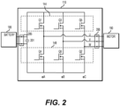
- FIG. 2 depicts an electrical power schematic of an inverter in a connected system, according to one or more embodiments.
- the inverter may be used to convert DC power from a battery in an electric vehicle to AC power, to drive an electric motor of the electric vehicle, for example, but the embodiments are not limited thereto. Additionally, the inverter may be bidirectional, and used to convert DC power to AC power, or to convert AC power to DC power.
- inverter 110 may be connected to battery 195 (DC power supply) and motor 190.
- Inverter 110 may include upper phase switches 144 and lower phase switches 148 as components of a power module.
- a first phase ( ⁇ A) may include switches Q1 and Q4, a second phase ( ⁇ B) may include switches Q3 and Q6, and a third phase ( ⁇ C) may include switches Q5 and Q2, as illustrated in FIG. 2 .
- Upper phase switches 144 may include first phase switch Q1, second phase switch Q3, and third phase switch Q5.
- Lower phase switches 148 may include first phase switch Q4, second phase switch Q6, and third phase switch Q2.
- Switches Q1-Q6 may be metal-oxide-semiconductor field-effect transistors (MOSFET), for example, but are not limited thereto.
- MOSFET metal-oxide-semiconductor field-effect transistors
- FIG. 2 illustrates a three-phase inverter, the disclosure is not limited thereto, and may include single phase or multi-phase or multi-level inverters.
- Upper phase switches 144 and lower phase switches 148 may be driven by a PWM signal generated by one or more controllers to convert DC power delivered via the set of input terminals 285 at bulk capacitor 201 to three phase AC power at outputs U, V, and W (correlating with phases A, B, and C, respectively) via the set of output terminals 295 to motor 190.
- the bulk capacitor 201 may be referred to as the capacitor components of a bulk capacitor assembly, for which various embodiments are disclosed.
- FIG. 2 illustrates a three-phase inverter, the disclosure is not limited thereto, and may include single phase or multi-phase or multi-level inverters.
- FIG. 3 depicts an exploded view of a power module and a heat sink assembly for an inverter, according to one or more embodiments.
- power module 330 may be compatible with the inverter 110 shown in FIGS. 1 and 2 , and may be used for switching operations for the inverter 110. As depicted, the power module 330 is between a first cooling channel 323 and a second cooling channel 326 of a heat sink assembly 320.
- the power module 330 may include one or more silicon carbide (SiC)-based power modules that deliver relatively high power densities and efficiencies needed to extend battery range and performance, although other semiconductor switches may be relied upon.
- SiC silicon carbide
- the power module 330 may contain circuitry and components configured to convert direct current (DC) from the electric vehicle battery to alternating current (AC) current (and vice versa), which can be utilized by the motor 190, for example, that drives the propulsion system.
- the power module 330 may be installed on one or more power board assemblies.
- the power module 330 may include a combination of transistors, diodes, metal oxide semiconductor field effect transistors (MOSFETs), insulated-gate bipolar transistors (IGBTs), and silicon-controlled rectifiers (SCRs).
- the power module 330 may include a combination of transistors configured to both a half-bridge and H-bridge configuration, which may allow for the switch ability of the direction of the current through a motor from a single voltage power supply.
- the power module 330 may also include three or more transistors for inverting applications such as switching direct current (DC) electricity into alternating current (AC) electricity.
- the first cooling channel 323 and the second cooling channel 326 may provide cooling for the power module 330, the bulk capacitor 201, and a stacked busbar (see FIG. 4 ) connectable to the power module 330 and the bulk capacitor 201.
- the stacked busbar may include a first side and a second side, the first side including one or more first capacitors thereon, and the second side including one or more second capacitors thereon.
- the one or more first capacitors may be electrically connected to the power module 330 via the first side of the stacked busbar.
- the one or more second capacitors may be electrically connected to the power module 330 via the second side of the stacked busbar.
- the first cooling channel 323 may provide cooling to a first side of the stacked busbar and one or more first capacitors provided on the first side of the stacked busbar.
- the second cooling channel 326 may provide cooling to a second side of the stacked busbar and one or more second capacitors provided on the second side of the stacked busbar.
- the first cooling channel 323 may physically couple to the first side of the stacked busbar, and the second cooling channel 326 may physically couple to the second side of the stacked busbar, for providing adequate cooling to the above-mentioned components.
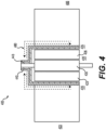
- FIG. 4 depicts a cross-sectional view of a bulk capacitor assembly for an inverter, according to one or more embodiments.
- bulk capacitor assembly 400 includes one or more first capacitors 403, one or more second capacitors 406, a stacked busbar 435 including a first DC busbar 440 and a second DC busbar 443, a heat sink assembly 420 including a first cooling channel 423 and a second cooling channel 426, and a power module 430 positioned between the first cooling channel 423 and the second cooling channel 426.
- the bulk capacitor assembly 400 may include the bulk capacitor 201.
- the bulk capacitor assembly 400 may be used in the inverter 110, for example.
- the heat sink assembly 420 may be similar to or interchangeable with the heat sink assembly 320.
- the power module 430 may be similar to or interchangeable with the power module 330.
- the stacked busbar 435 may include laminated busbar assemblies.
- the one or more first capacitors 403 may include one or more capacitor bobbins arranged on a first side of the stacked busbar 435.
- the one or more second capacitors 406 may include one or more capacitor bobbins arranged on a second side of the stacked busbar 435, where the second side is opposite to the first side.
- the one or more first capacitors 403 and the one or more second capacitors 406 may include various types of capacitors such as metalized polypropylene capacitors, ceramic capacitors, NanoLam TM based capacitors, and other types of capacitors.
- the first DC busbar 440 and the second DC busbar 443 are stacked closely together to support the arrangement of the one or more first capacitors 403 and the one or more second capacitors 406 on the first side of the stacked busbar 435 and the second side of the stacked busbar 435, respectively.
- the one or more first capacitors 403 and the one or more second capacitors 406 may be configured to electrically connect to both the first DC busbar 440 and the second DC busbar 443, the details of which will be discussed with respect to the later figures.
- first DC busbar 440 and the second DC busbar 443 may receive electrical power from a DC power supply (e.g., the battery 195) to transfer power to the connected components, such as the power module 430, the one or more first capacitors 403, and the one or more second capacitors 406.
- the first DC busbar 440 may be connected to a positive pole of a DC battery
- the second DC busbar 443 may be connected to a negative pole of the DC battery, or vice versa.
- the first cooling channel 423 and the second cooling channel 426 of the heat sink assembly 420 may provide cooling to the stacked busbar 435, the one or more first capacitors 403, the one or more second capacitors 406, and the power module 430.
- the first cooling channel 423 may provide cooling to the first side of the stacked busbar 435, a first side of the power module 430, and the one or more first capacitors 403.
- the second cooling channel 426 may provide cooling to the second side of the stacked busbar 435, a second side of the power module 430, and the one or more second capacitors 406.
- the power module 430 may include similar components as the power module 330 and may include one or more silicon carbide (SiC)-based power modules that deliver relatively high power densities and efficiencies needed to extend battery range and performance, although other semiconductor switches may be relied upon.
- the power module 430 may contain circuitry and components configured to convert direct current (DC) from the electric vehicle battery to alternating current (AC) current (and vice versa), which can be utilized by the motor 190, for example, that drives the propulsion system.
- the power module 430 may be installed on one or more power board assemblies.
- the power module 430 may include a combination of transistors, diodes, metal oxide semiconductor field effect transistors (MOSFETs), insulated-gate bipolar transistors (IGBTs), and silicon-controlled rectifiers (SCRs).
- the power module 430 may include a combination of transistors configured to both a half-bridge and H-bridge configuration, which may allow for the switch ability of the direction of the current through a motor from a single voltage power supply.
- the power module 430 may also include three or more transistors for inverting applications such as switching direct current (DC) electricity into alternating current (AC) electricity.
- electrical current may be configured to flow in a loop 480 as depicted, where the one or more first capacitors 403 may connect to the one or more second capacitors 406 in a parallel configuration.
- the power module 430 may be positioned between the first side of the stacked busbar 435 and the second side of the stacked busbar 435.
- FIG. 5 depicts a side view of a bulk capacitor assembly for an inverter, according to one or more embodiments.
- bulk capacitor assembly 500 may include many of the same components as the bulk capacitor assembly 400 and may be interchangeable with the bulk capacitor assembly 400.
- the bulk capacitor assembly 500 includes a stacked busbar 535, which includes a first DC busbar 540 and a second DC busbar 543.
- the stacked busbar 535 may include laminated busbar assemblies.
- the first DC busbar 540 may be connected to a positive pole of a DC battery (e.g., battery 195), and the second DC busbar may be connected to a negative pole of the DC battery, or vice versa.
- the stacked busbar 535 may be used to transfer electrical power from the battery 195 to a connectable power module and one or more DC-link capacitors connected to the stacked busbar 535.
- FIG. 5 depicts one or more first capacitors 503 provided on a first side of stacked busbar 535.
- the bulk capacitor assembly 500 may include one or more second capacitors provided on a second side of the stacked busbar 535, similar to bulk capacitor assembly 400, although not depicted in FIG. 5 .
- the one or more first capacitors 503 may include one or more first and second capacitors connected in series.
- the one or more first capacitors 503 may include a first capacitor 506 connected in series to a second capacitor 509 with a first conductive plate 507, a first capacitor 512 connected in series to a second capacitor 515 with a second conductive plate 513, a first capacitor 518 connected in series to a second capacitor 521 with a third conductive plate 520, and a first capacitor 524 connected in series to a second capacitor 527 with a fourth conductive plate 525.
- FIG. 5 depicts four first and second capacitors connected in series, this disclosure is not limited thereto. Fewer or greater than four first and second capacitors may be implemented depending on the application for use of the bulk capacitor assembly 500.
- the first DC busbar 540 and the second DC busbar 543 are stacked closely together to support the arrangement of the one or more first capacitors 503 on the first side of the stacked busbar 535.
- the one or more first capacitors 503 may be electrically connected to both the first DC busbar 540 and the second DC busbar 543, the details of which will be discussed with respect to the later figures.
- the first DC busbar 540 and the second DC busbar 543 may receive electrical power from a DC power supply (e.g., the battery 195) to transfer power to the connected components, such as a power module, the one or more first capacitors 503.
- the first DC busbar 540 may be connected to a positive pole of a DC battery, and the second DC busbar 543 may be connected to a negative pole of the DC battery, or vice versa.
- the bulk capacitor assembly 500 may facilitate flow 531 of electrical current between the stacked busbar 535 and the one or more first capacitors 503.
- components of the bulk capacitor assembly 500 may be arranged and electrically connected so that for the first capacitors (e.g., the first capacitor 506, the first capacitor 512, the first capacitor 518, and the first capacitor 524) and the second capacitors (e.g., the second capacitor 509, the second capacitor 515, the second capacitor 521, and the second capacitor 527) connected in series, electrical current may be follow flow 531.
- the first capacitors e.g., the first capacitor 506, the first capacitor 512, the first capacitor 518, and the first capacitor 52
- the second capacitors e.g., the second capacitor 509, the second capacitor 515, the second capacitor 521, and the second capacitor 527 connected in series
- electrical current may follow flow 531 from the first DC busbar 540, through second capacitor 527, through fourth conductive plate 525, through first capacitor 524, and to the second DC busbar 543.
- the electrical current may be configured to follow flow 531 in a current loop in parallel through the four first and second capacitors connected in series.
- FIG. 6 depicts an exploded view of a bulk capacitor assembly for an inverter with a heat sink, a power module, and a printed circuit board, according to one or more embodiments.
- bulk capacitor assembly 600 may be similar to the bulk capacitor assembly 400 and the bulk capacitor assembly 500 and may include many of the same components as the bulk capacitor assembly 400 and the bulk capacitor assembly 500. Additionally, many of the components of the bulk capacitor assembly 400 and the bulk capacitor assembly 500 may be interchangeable with the components of the bulk capacitor assembly 600.
- the bulk capacitor assembly 600 includes a stacked busbar 635, which includes a first DC busbar 640 and a second DC busbar 643. Although FIG. 6 illustrates an exploded view, the first DC busbar 640 and the second DC busbar 643 may be electrically connected as a final assembly.
- the bulk capacitor assembly 600 further includes one or more first capacitors 603 provided on a first side of the stacked busbar 635, one or more second capacitors 606 provided on a second side of the stacked busbar 635, a heat sink assembly 653 positioned between the one or more first capacitors 603 and the one or more second capacitors 606, and a printed circuit board (PCB) 650 extending across the first side of the stacked busbar 635 and the second side of the stacked busbar 635.
- the first side of the stacked busbar 635 and the second side of the stacked busbar 635 may be separable components that may be coupled together via a welding process, for example.
- the one or more first capacitors 603 and the one or more second capacitors 606 may be contained within a protective housing 693.
- a power module 630 may be positioned between a first cooling channel 623 and a second cooling channel 626 of the heat sink assembly 653, similar to how the power module 330 is positioned between the first cooling channel 323 and the second cooling channel 326 (depicted in FIG. 3 ).
- the power module 630 may be positioned between the first side of the stacked busbar 635 and the second side of the stacked busbar 635.
- the one or more first capacitors 603 provided on the first side of the stacked busbar 635 may be electrically connected to the power module 330 via the first side of the stacked busbar 635.
- the one or more second capacitors 606 provided on the second side of the stacked busbar 635 may be electrically connected to the power module 330 via the second side of the stacked busbar 635.
- the first DC busbar 640 and the second DC busbar 643 are stacked closely together to support the arrangement of the one or more first capacitors 603 and the one or more second capacitors 606 on the first side of the stacked busbar 635 and the second side of the stacked busbar 635, respectively.
- an insulation material 627 may separate the first DC busbar 640 from the second DC busbar 643.
- the one or more first capacitors 603 and the one or more second capacitors 606 may be configured to electrically connect to both the first DC busbar 640 and the second DC busbar 643, which will be discussed in the following paragraphs.
- first DC busbar 640 and the second DC busbar 643 may receive electrical power from a DC power supply (e.g., the battery 195) to transfer power to the connected components, such as the power module 630, the one or more first capacitors 603, and the one or more second capacitors 606.
- the first DC busbar 640 may be connected to a positive pole of a DC battery
- the second DC busbar 643 may be connected to a negative pole of the DC battery, or vice versa.
- One or more apertures may be provided in the first DC busbar 640 and the second DC busbar 643.
- one or more first apertures in the first DC busbar 640 on the first side of the stacked busbar 635 may include a first aperture 680, a second aperture 682, a third aperture 684, a fourth aperture 686, a fifth aperture 688, and a sixth aperture 690.
- the second DC busbar 643 may include one or more second apertures corresponding to the one or more first apertures.
- the one or more second apertures may be similar in size to the size of the one or more first apertures. In some cases, the one or more second apertures may be smaller in size than the size of the one or more first apertures.
- first aperture 680 may be an isolation aperture in first DC busbar 640 corresponding to a connection aperture in second DC busbar 643
- second aperture 682 may be a connection aperture in first DC busbar 640 corresponding to a through aperture in second DC busbar 643.
- the first DC busbar 640 and the second DC busbar 643 at the second side of the stacked busbar 635 may include a same number of apertures as the number of apertures on the first side, in a mirror configuration, for facilitating an electrical connection of a capacitor of the one or more second capacitors 606 to the first DC busbar 640 or the second DC busbar 643.
- the first cooling channel 623 and the second cooling channel 626 may be coupled together to provide cooling for the power module 630, the one or more first capacitors 603, the one or more second capacitors 606, and the stacked busbar 635.
- the first cooling channel 623 may provide cooling to the first side of the stacked busbar 635 and the one or more first capacitors 603.
- the second cooling channel 626 may provide cooling to the second side of the stacked busbar 635 and the one or more second capacitors 606.
- the first cooling channel 623 may physically couple to the first side of the stacked busbar 635
- the second cooling channel 626 may physically couple to the second side of the stacked busbar 635 for providing adequate cooling to the above-mentioned components.
- One or more apertures 673, 676, and 679 may be provided on the PCB 650 for receiving connectors of the power module 630.
- the PCB 650 may facilitate connection of the power module 630 to a motor (e.g., the motor 190) and one or more controllers or circuits that may control switching operations of the power module 630.
- FIGS. 7A and 7B depict a top view and a bottom view, respectively, of one or more first capacitors provided on a stacked busbar, according to one or more embodiments.
- FIG. 7A depicts a top view of the one or more first capacitors 603 on a first side of the stacked busbar 635 without the protective housing 693.
- the one or more first capacitors 603 may include one or more first and second capacitors connected in series.
- the one or more first capacitors 603 may include a first capacitor 608 connected in series to a second capacitor 609 with a first conductive plate 607 and a first capacitor 612 connected in series to a second capacitor 615 with a second conductive plate 613.
- FIG. 7A depicts two first and second capacitors connected in series, this disclosure is not limited thereto. Fewer or greater than two first and second capacitors may be implemented depending on the application for use of the bulk capacitor assembly 600.
- the first capacitor may be electrically connected to the first DC busbar 640, and the second capacitor may be electrically connected to a second DC busbar 643, or vice versa, by way of a respective aperture or window of the one or more first apertures provided for the first DC busbar 640 on the first side of the stacked busbar 635.
- the first capacitor 608 may be electrically connected to the second DC busbar 643 at the first aperture 680
- the second capacitor 609 may be electrically connected to the first DC busbar 640 through the second aperture 682.
- the first capacitor 608 and the second capacitor 609 may be electrically connected with the first conductive plate 607. Based on these connections, electrical current may be configured to flow from the second DC busbar 643, through the first capacitor 608, through the first conductive plate 607, through the second capacitor 609, and to the first DC busbar 640. In some cases, electrical current may be configured to flow from the first DC busbar 640, through the second capacitor 609, through the first conductive plate 607, through the first capacitor 608, and to the second DC busbar 643. The flow of electrical current described above may result in a smaller current loop between the interconnected components.
- FIG. 7B depicts a bottom view of the one or more first capacitors 603 on a first side of the stacked busbar 635 without the protective housing 693.
- the first capacitor 608 is electrically connected to the second capacitor 609 in a series configuration by the first conductive plate 607
- the first capacitor 612 is connected to the second capacitor 615 in a series configuration by the second conductive plate 613.
- the first capacitor may be electrically connected to a first DC busbar, and the second capacitor may be electrically connected to a second DC busbar, or vice versa, by way of a respective aperture of the one or more first apertures provided for the first DC busbar 640 on the first side of the stacked busbar 635.
- FIG. 8 depicts a portion of a bulk capacitor assembly for a first mounting stage, according to one or more embodiments.
- FIG. 8 depicts a portion of the bulk capacitor assembly 600 including the heat sink assembly 653, the power module 630, and the one or more first capacitors 603.
- the one or more first capacitors 603 may first be placed on a mounting jig.
- the heat sink assembly 653 with the power module 630 may be aligned and placed on the one or more first capacitors 603 as depicted.
- each connector of the connector pairs 818, 821, and 824 of the power module 630 may connect to the first DC busbar 640 and/or the second DC busbar 643, respectively.
- Connectors 809, 812, and 815 of the power module 630 may connect to respective phases of a motor, such as the motor 190.
- FIG. 9 depicts a portion of a bulk capacitor assembly for a second mounting stage, according to one or more embodiments.
- FIG. 9 depicts a portion of the bulk capacitor assembly 600 including the heat sink assembly 653, the power module 630, the one or more first capacitors 603, and the one or more second capacitors 606.
- the one or more second capacitors 606 may be connected to the heat sink assembly 653, the power module 630, and the one or more first capacitors 603.
- the first cooling channel 623 may be mounted or coupled to the one or more first capacitors 603.
- the second cooling channel 626 may be mounted or coupled to the one or more second capacitors 606.
- FIG. 10 depicts a portion of a bulk capacitor assembly for a laser welding stage, according to one or more embodiments.
- FIG. 10 depicts a portion of the bulk capacitor assembly 600 including the one or more first capacitors 603 and the one or more second capacitors 606.
- Terminals 1003 of the first DC busbar 640 and the second DC busbar 643 of the first side and the second side of the stacked busbar 635 may be laser welded together to electrically connect the first side and the second side of the stacked busbar 635 and the power module 630.
- the one or more first capacitors 603 may be connected to the one or more second capacitors 606 in a parallel configuration.
- FIG. 11 depicts a finalized bulk capacitor assembly for an inverter, according to one or more embodiments.
- the bulk capacitor assembly 600 may include the one or more first capacitor 603, the one or more second capacitor 606, the stacked busbar 635, which includes the first DC busbar 640 and the second DC busbar 643, the heat sink assembly 653, the power module 630, and the PCB 650.
- the PCB 650 may extend across the first side and the second side of the stacked busbar 635.
- the PCB 650 may facilitate a connection of the connectors 809, 812, and 815 of the power module 630 to a motor, such as the motor 190.
- the PCB 650 may facilitate a connection of one or more controllers or circuits that may control switching operations of the power module 630.
- One or more embodiments as described in this disclosure may reduce the parasitic inductance of the switching loop involving a power module, which may reduce switching power loss.
- the power modules having a reduced semiconductor area may have the same performance as other power modules having a larger semiconductor area.
- One or more embodiments may reduce parasitic inductance of the power module and enable EMC compliance with minimal efforts.
- One or more embodiments may provide robust DC-link capacitors due to active cooling available on both sides of the power module.
Landscapes
- Engineering & Computer Science (AREA)
- Power Engineering (AREA)
- Microelectronics & Electronic Packaging (AREA)
- Physics & Mathematics (AREA)
- Thermal Sciences (AREA)
- Inverter Devices (AREA)
Applications Claiming Priority (1)
| Application Number | Priority Date | Filing Date | Title |
|---|---|---|---|
| US18/448,718 US20250055385A1 (en) | 2023-08-11 | 2023-08-11 | Systems and methods for lower commutation loop inductance bulk capacitor |
Publications (1)
| Publication Number | Publication Date |
|---|---|
| EP4507183A1 true EP4507183A1 (fr) | 2025-02-12 |
Family
ID=91958782
Family Applications (1)
| Application Number | Title | Priority Date | Filing Date |
|---|---|---|---|
| EP24189131.6A Pending EP4507183A1 (fr) | 2023-08-11 | 2024-07-17 | Systèmes et procédés pour condensateur de stabilisation à inductance de commutation inférieure |
Country Status (3)
| Country | Link |
|---|---|
| US (1) | US20250055385A1 (fr) |
| EP (1) | EP4507183A1 (fr) |
| CN (1) | CN119519450A (fr) |
Families Citing this family (1)
| Publication number | Priority date | Publication date | Assignee | Title |
|---|---|---|---|---|
| US20250300569A1 (en) * | 2024-03-20 | 2025-09-25 | Ford Global Technologies, Llc | Power module for electrified vehicle |
Citations (10)
| Publication number | Priority date | Publication date | Assignee | Title |
|---|---|---|---|---|
| JPH10201249A (ja) * | 1996-12-27 | 1998-07-31 | Shinko Electric Co Ltd | 3レベルインバータのパワーモジュールスタック |
| JP2007006584A (ja) * | 2005-06-22 | 2007-01-11 | Mitsubishi Electric Corp | 電力変換装置 |
| US20110149625A1 (en) * | 2005-11-17 | 2011-06-23 | Hitachi, Ltd. | Capacitor Module, Power Converter, Vehicle-Mounted Electrical-Mechanical System |
| US20120044640A1 (en) * | 2009-07-06 | 2012-02-23 | Mitsubishi Electric Corporation | Power converter |
| JP5073530B2 (ja) * | 2008-02-25 | 2012-11-14 | 株式会社日立製作所 | 電力変換器の主回路構造 |
| JP6609928B2 (ja) * | 2015-01-28 | 2019-11-27 | 株式会社明電舎 | コンデンサの取付構造及び電力変換装置 |
| EP3893615A1 (fr) * | 2020-04-07 | 2021-10-13 | Hamilton Sundstrand Corporation | Ensembles convertisseurs de puissance avec barres omnibus |
| JP7065595B2 (ja) * | 2017-12-13 | 2022-05-12 | 株式会社Soken | フィルムコンデンサモジュール |
| WO2022179966A1 (fr) * | 2021-02-24 | 2022-09-01 | Danfoss Silicon Power Gmbh | Structure de conducteur |
| WO2022239170A1 (fr) * | 2021-05-13 | 2022-11-17 | 三菱電機株式会社 | Dispositif de conversion de puissance |
Family Cites Families (8)
| Publication number | Priority date | Publication date | Assignee | Title |
|---|---|---|---|---|
| DE4412990A1 (de) * | 1994-04-15 | 1995-10-19 | Abb Patent Gmbh | Stromrichteranlage mit flüssigkeits- oder luftgekühlten Leistungshalbleitern und Gleichspannungszwischenkreis |
| US5729450A (en) * | 1995-06-14 | 1998-03-17 | Magnetek, Inc. | Power converter with ripple current and bulk filtering supplied by high-current, high-microfarad film capacitor arrangement |
| US6160696A (en) * | 1998-05-04 | 2000-12-12 | General Electric Company | Modular bus bar and switch assembly for traction inverter |
| US11070049B2 (en) * | 2017-11-08 | 2021-07-20 | Eaton Intelligent Power Limited | System, method, and apparatus for power distribution in an electric mobile application using a combined breaker and relay |
| US11464138B2 (en) * | 2019-04-22 | 2022-10-04 | Transportation Ip Holdings, Llc | Module panel and method for an electrical power delivery system |
| JP7280124B2 (ja) * | 2019-06-26 | 2023-05-23 | ファナック株式会社 | 2つの直流電圧モードを有する電力変換装置及びモータ駆動装置 |
| EP4145143B1 (fr) * | 2020-04-27 | 2025-08-13 | LG Magna e-Powertrain Co., Ltd. | Ensemble capteur de courant |
| US20240006125A1 (en) * | 2022-06-30 | 2024-01-04 | Tdk Electronics Ag | Metallized Film DC-Link High Power Capacitors for High Frequency Applications |
-
2023
- 2023-08-11 US US18/448,718 patent/US20250055385A1/en active Pending
-
2024
- 2024-07-17 EP EP24189131.6A patent/EP4507183A1/fr active Pending
- 2024-08-08 CN CN202411083984.4A patent/CN119519450A/zh active Pending
Patent Citations (10)
| Publication number | Priority date | Publication date | Assignee | Title |
|---|---|---|---|---|
| JPH10201249A (ja) * | 1996-12-27 | 1998-07-31 | Shinko Electric Co Ltd | 3レベルインバータのパワーモジュールスタック |
| JP2007006584A (ja) * | 2005-06-22 | 2007-01-11 | Mitsubishi Electric Corp | 電力変換装置 |
| US20110149625A1 (en) * | 2005-11-17 | 2011-06-23 | Hitachi, Ltd. | Capacitor Module, Power Converter, Vehicle-Mounted Electrical-Mechanical System |
| JP5073530B2 (ja) * | 2008-02-25 | 2012-11-14 | 株式会社日立製作所 | 電力変換器の主回路構造 |
| US20120044640A1 (en) * | 2009-07-06 | 2012-02-23 | Mitsubishi Electric Corporation | Power converter |
| JP6609928B2 (ja) * | 2015-01-28 | 2019-11-27 | 株式会社明電舎 | コンデンサの取付構造及び電力変換装置 |
| JP7065595B2 (ja) * | 2017-12-13 | 2022-05-12 | 株式会社Soken | フィルムコンデンサモジュール |
| EP3893615A1 (fr) * | 2020-04-07 | 2021-10-13 | Hamilton Sundstrand Corporation | Ensembles convertisseurs de puissance avec barres omnibus |
| WO2022179966A1 (fr) * | 2021-02-24 | 2022-09-01 | Danfoss Silicon Power Gmbh | Structure de conducteur |
| WO2022239170A1 (fr) * | 2021-05-13 | 2022-11-17 | 三菱電機株式会社 | Dispositif de conversion de puissance |
Also Published As
| Publication number | Publication date |
|---|---|
| US20250055385A1 (en) | 2025-02-13 |
| CN119519450A (zh) | 2025-02-25 |
Similar Documents
| Publication | Publication Date | Title |
|---|---|---|
| KR102868246B1 (ko) | 다중 출력을 가진 멀티브리지 전력 컨버터 | |
| EP2660967B1 (fr) | Appareil de conversion de puissance | |
| CN101411050B (zh) | 电力变换装置及其装配方法 | |
| CN101681898B (zh) | 半导体元件的冷却构造 | |
| EP2660966A1 (fr) | Appareil de conversion de puissance pour véhicule | |
| CA3067320C (fr) | Dispositif de conversion d'energie | |
| US8493762B2 (en) | Power semiconductor module and semiconductor power converter provided with the same | |
| WO2012132687A1 (fr) | Onduleur | |
| CN103597732A (zh) | 电力转换装置 | |
| US11128235B2 (en) | Power conversion device | |
| EP3817046B1 (fr) | Unité d'élément de commutation et module d'élément de commutation | |
| CN112448651A (zh) | 操作车辆的电动驱动器的控制器和制造该控制器的方法 | |
| CN112821796A (zh) | 用于车辆的电动驱动器的电子模块 | |
| EP4507183A1 (fr) | Systèmes et procédés pour condensateur de stabilisation à inductance de commutation inférieure | |
| CN112152471A (zh) | 用于电源装置的集成功率单元 | |
| US20240072030A1 (en) | Semiconductor power module having more efficient heat dissipation and improved switching behavior | |
| CN217935444U (zh) | 电力转换装置、马达模块及车辆 | |
| EP4503424A1 (fr) | Ensemble condensateur pour onduleur pour véhicule électrique | |
| CN117318489A (zh) | 功率转换装置 | |
| US20250386472A1 (en) | Systems for housing pockets for inverter for electric vehicle | |
| US12323070B2 (en) | Power conversion device | |
| US12355380B2 (en) | Inverter structure of an inverter of a power electronics module for operating an electric drive of a motor vehicle | |
| EP4665093A1 (fr) | Systèmes de condensateur pour onduleur pour véhicule électrique | |
| US20250357362A1 (en) | Semiconductor apparatus and power conversion apparatus |
Legal Events
| Date | Code | Title | Description |
|---|---|---|---|
| PUAI | Public reference made under article 153(3) epc to a published international application that has entered the european phase |
Free format text: ORIGINAL CODE: 0009012 |
|
| STAA | Information on the status of an ep patent application or granted ep patent |
Free format text: STATUS: THE APPLICATION HAS BEEN PUBLISHED |
|
| AK | Designated contracting states |
Kind code of ref document: A1 Designated state(s): AL AT BE BG CH CY CZ DE DK EE ES FI FR GB GR HR HU IE IS IT LI LT LU LV MC ME MK MT NL NO PL PT RO RS SE SI SK SM TR |
|
| STAA | Information on the status of an ep patent application or granted ep patent |
Free format text: STATUS: REQUEST FOR EXAMINATION WAS MADE |
|
| 17P | Request for examination filed |
Effective date: 20250324 |
|
| P01 | Opt-out of the competence of the unified patent court (upc) registered |
Free format text: CASE NUMBER: UPC_APP_0002973_4507183/2026 Effective date: 20260128 |
|
| STAA | Information on the status of an ep patent application or granted ep patent |
Free format text: STATUS: EXAMINATION IS IN PROGRESS |