EP4507204A1 - Système de sélection d'au moins un canal fréquentiel dans un signal d'entrée, récepteur et circuit intégré correspondants - Google Patents
Système de sélection d'au moins un canal fréquentiel dans un signal d'entrée, récepteur et circuit intégré correspondants Download PDFInfo
- Publication number
- EP4507204A1 EP4507204A1 EP23306368.4A EP23306368A EP4507204A1 EP 4507204 A1 EP4507204 A1 EP 4507204A1 EP 23306368 A EP23306368 A EP 23306368A EP 4507204 A1 EP4507204 A1 EP 4507204A1
- Authority
- EP
- European Patent Office
- Prior art keywords
- capacitor
- clocks
- sampling
- output
- reset
- Prior art date
- Legal status (The legal status is an assumption and is not a legal conclusion. Google has not performed a legal analysis and makes no representation as to the accuracy of the status listed.)
- Pending
Links
- 239000003990 capacitor Substances 0.000 claims abstract description 104
- 238000005070 sampling Methods 0.000 claims abstract description 51
- 230000000737 periodic effect Effects 0.000 claims description 10
- 241001248035 Trigonidiinae Species 0.000 claims description 8
- 230000001960 triggered effect Effects 0.000 claims description 3
- 230000002776 aggregation Effects 0.000 description 4
- 238000004220 aggregation Methods 0.000 description 4
- 238000001914 filtration Methods 0.000 description 4
- 238000001228 spectrum Methods 0.000 description 4
- 230000000694 effects Effects 0.000 description 2
- 238000005516 engineering process Methods 0.000 description 2
- 230000001747 exhibiting effect Effects 0.000 description 2
Images



Classifications
-
- H—ELECTRICITY
- H04—ELECTRIC COMMUNICATION TECHNIQUE
- H04B—TRANSMISSION
- H04B1/00—Details of transmission systems, not covered by a single one of groups H04B3/00 - H04B13/00; Details of transmission systems not characterised by the medium used for transmission
- H04B1/005—Details of transmission systems, not covered by a single one of groups H04B3/00 - H04B13/00; Details of transmission systems not characterised by the medium used for transmission adapting radio receivers, transmitters andtransceivers for operation on two or more bands, i.e. frequency ranges
- H04B1/0053—Details of transmission systems, not covered by a single one of groups H04B3/00 - H04B13/00; Details of transmission systems not characterised by the medium used for transmission adapting radio receivers, transmitters andtransceivers for operation on two or more bands, i.e. frequency ranges with common antenna for more than one band
- H04B1/006—Details of transmission systems, not covered by a single one of groups H04B3/00 - H04B13/00; Details of transmission systems not characterised by the medium used for transmission adapting radio receivers, transmitters andtransceivers for operation on two or more bands, i.e. frequency ranges with common antenna for more than one band using switches for selecting the desired band
-
- H—ELECTRICITY
- H04—ELECTRIC COMMUNICATION TECHNIQUE
- H04B—TRANSMISSION
- H04B1/00—Details of transmission systems, not covered by a single one of groups H04B3/00 - H04B13/00; Details of transmission systems not characterised by the medium used for transmission
- H04B1/005—Details of transmission systems, not covered by a single one of groups H04B3/00 - H04B13/00; Details of transmission systems not characterised by the medium used for transmission adapting radio receivers, transmitters andtransceivers for operation on two or more bands, i.e. frequency ranges
- H04B1/0053—Details of transmission systems, not covered by a single one of groups H04B3/00 - H04B13/00; Details of transmission systems not characterised by the medium used for transmission adapting radio receivers, transmitters andtransceivers for operation on two or more bands, i.e. frequency ranges with common antenna for more than one band
- H04B1/0057—Details of transmission systems, not covered by a single one of groups H04B3/00 - H04B13/00; Details of transmission systems not characterised by the medium used for transmission adapting radio receivers, transmitters andtransceivers for operation on two or more bands, i.e. frequency ranges with common antenna for more than one band using diplexing or multiplexing filters for selecting the desired band
-
- H—ELECTRICITY
- H04—ELECTRIC COMMUNICATION TECHNIQUE
- H04B—TRANSMISSION
- H04B1/00—Details of transmission systems, not covered by a single one of groups H04B3/00 - H04B13/00; Details of transmission systems not characterised by the medium used for transmission
- H04B1/06—Receivers
- H04B1/16—Circuits
Definitions
- the field of the disclosure is that of the processing of a signal received by a receiver device.
- the disclosure relates to a system for the selection of one (or more) frequency channel(s) in such signal.
- the disclosure can be of interest in any field wherein the selection of one (or more) frequency channel(s) in a received signal is of interest. This can be the case e.g. in the field of receivers for radars, for sonars, or for wireless communications, e.g. receivers for 5G, 3GPP LTE Pro, LiFi, and "Beyond 5G" standards), LAN (for "Local Area Network”), Home-area networks, etc.
- harmonic rejection N-path filters HR-NPF
- harmonic rejection N-path mixers HR-NPM
- the article from AL Shakoush, A. & Lauga-Larroze, Estelle & Subias, S. & Taris, T. & Podevin, Florence & Bourdel, S. "Low Complexity Architecture of N-Path Mixers for Low Power Application” 17th IEEE International New Circuits and Systems Conference (NEWCAS), 2019 describes such HR-NPM which is also illustrated in Figure 1 and Figure 1a .
- the receiving antenna is represented through its equivalent electrical circuit comprising the voltage source V s and the internal resistor R that thus delivers a current proportional to the received input signal.
- the HR-NPM 100 comprises:
- the ON state of a clock corresponds to the state that turns ON the switch that is trigged by the clock in question.
- the ON state of a clock that trigs a NMOS type transistor is the high voltage level of the clock.
- the ON state of a clock that trigs a PMOS type transistor is the low voltage level of the clock.
- each path 120 comprises:
- such HR-NPM 100 filters the spectrum of the input signal and further translates in frequency such spectrum by an amount equal to 1/T LO .
- the N respective sampled waveforms associated to the N paths are the H first samples (or, equivalently, the H successive samples starting from a same given sample index (i.e. the H successive samples starting from the first sample, or from the second sample, or from the third sample, etc.) as it leads to the same set of N sampled waveforms in any case) of the N circular permutations of a sampled pattern obtained by N successive time shifts of a sampling period T LO /N.
- the sampled pattern is chosen so as to minimize the level of the harmonics at multiples of the frequency 1/T LO (i.e.
- the sampled pattern corresponds to samples of a sinewave of period T LO as given by equation (2) in the above-mentioned article.
- the center frequency provided by such filtering is not flexible, at least independently of the tuning of the sampling clocks frequency 1/T LO .
- the transfer function does not provide flexibility in its shape so that no more than one frequency channel can be selected simultaneously.
- a particular aspect of the present disclosure relates to a system for the selection of at least one frequency channel in an input signal.
- Such system comprises:
- the present disclosure proposes a new and inventive solution for selecting (e.g. through filtering and/or downmixing) one (or more) frequency channel(s) in a signal in a flexible way.
- the reset, at each period of the sampling clocks, of the voltage across the output capacitors of the N paths of a structure of the HR-NPF or HR-NPM type allows implementing a sampled pattern that does not need to be a periodic function of the sampling clocks period T LO .
- This thus allows flexibility in the shape for the transfer function of the system. For instance, a transfer function exhibiting a bandpass behavior centered around the frequency channel(s) to be selected can be implemented.
- the sampled pattern corresponds to the sampling of a sinewave.
- a frequency of the sinewave is different from 1/T LO .
- the at least one frequency channel comprises a frequency channel centered on the frequency of the sinewave.
- the transfer function of the system exhibits a bandpass behavior centered around the frequency channel corresponding to the frequency of the sinewave.
- the sampled pattern corresponds to the sampling of a sum of sinewaves.
- the at least one frequency channel comprises, for each sinewave, a frequency channel centered on the frequency of the sinewave.
- the transfer function of the system exhibits a bandpass behavior centered around the frequency channels corresponding to the frequencies of the sinewaves.
- the selection (or aggregation) of the frequency channels corresponding to the frequencies of the sinewaves is thus obtained.
- the at least one capacitor comprises a first capacitor and a second capacitor.
- the at least one reset switch comprises:
- a capacitor is charged during the period T LO and then discharged during the next period.
- This decorrelation between charge and discharge relaxes the requirements in terms of timings. For instance, this avoids potential glitches in the clocks, as well as the loss of current that is necessarily not integrated into the capacitor during the reset duration when such reset occurs during the same T LO period than the charging of the capacitor.
- the at least one multiplexer comprises a first multiplexer and a second multiplexer.
- the output stage is configured for:
- the system comprises a reconstruction block comprising, for each path, a switch, hereafter output switch, configured to connect the output of the output stage to an output of the reconstruction block.
- the clock system delivers N non-overlapping periodic clocks, hereafter reconstruction clocks, shifted by a duration substantially equal to T LO /N in relation to each other, the period of the reconstruction clocks being T LO , a duration of a ON state of the reconstruction clocks being substantially equal to T LO /N.
- Each reconstruction clock trigs a respective output switch for having the output of the output stage provided to an output of the reconstruction block.
- the N output switches are trigged sequentially following a same ordering as the N sampled waveforms associated to the N paths when the sampled waveforms are ordered following the N successive time shifts of the sampling period T LO /N.
- the signal delivered at the output of the reconstruction block is up-converted back around the same center frequency as the input signal.
- the system thus behaves as a HR-NPF, but with the flexibility in the shape for the transfer function of the system.
- the reconstruction clocks and the sampling clocks are same clocks.
- Another aspect of the present disclosure relates to a receiver comprising a system for the selection of at least one frequency channel as discussed above (in any of the different embodiments discussed above).
- Another aspect of the present disclosure relates to an integrated circuit comprising a receiver comprising a system for the selection of at least one frequency channel as discussed above (in any of the different embodiments discussed above).
- each of the N processing paths 220 of the system 200 comprises an output stage 221 comprising:
- the output of the output stage 221 delivers the voltage present across the respective load capacitor C 1 or C 2 or ... or C N .
- the output of the output stage 221 is connected to the ungrounded terminal of the respective load capacitor C 1 or C 2 or ... or C N .
- each output stage 221 comprises more than one load capacitor C 1 or C 2 or ... or C N , e.g. as in the embodiment of Figure 4 discussed below.
- each output stage 221 comprises more than one reset switch, e.g. put in parallel of different load capacitors as in the embodiment of Figure 4 discussed below.
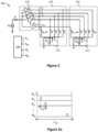
- the clock system 230 of the system 200 delivers, in addition to the N sampling clocks S 1 , S 2 , ..., S N , N clocks R 1 , R 2 , ..., R N , hereafter reset clocks.
- Each reset clock trigs a respective reset switch for resetting the voltage across the capacitor C 1 or C 2 or ... or C N once per period T LO .
- the reset, at each period T LO of the sampling clocks, of the voltage across the output capacitors C 1 , C 2 , ..., C N of the N paths allows implementing a sampled pattern that does not need to be a periodic function of the sampling clock period T LO .
- This provides flexibility in the shape for the transfer function of the system 200. For instance, a transfer function exhibiting a bandpass behavior centered around the frequency channel(s) to be selected can be implemented.
- the sampled pattern corresponds to the sampling of a sinewave.
- the H gain factors G h sin 2 ⁇ . F c N .
- the sampled pattern corresponds to the sampling of a sum of sinewaves.
- the aggregation of the frequency channels corresponding to the frequencies of the N c sinewaves is thus obtained.
- Figure 3 illustrates the modulus of the transfer function H ( f ) obtained for two sinewaves with frequencies F c 1 and F c 2 . More particularly:
- the system 200 according to this example can thus be used for the selection (or aggregation) of two frequency channels centered around the two frequencies F c 1 and F c 2 .
- the load capacitors are chosen as 50pF.
- the present technic allows achieving a transfer function that exhibits a filtering effect around the two frequencies F c 1 and F c 2 thus allowing the selection (or aggregation) of the two corresponding frequency channels.
- the capacitor C 1 or C 2 or ... or C N is charged during a T LO time interval and then discharged, ready for the next cycle of charge and discharge during the next T LO time interval.
- the voltage at the capacitor C 1 or C 2 or ... or C N is then refreshed at each sampling clocks period T LO .
- there may be a loss in the current that is necessarily not integrated into said capacitor C 1 or C 2 or ... or C N during the reset duration.
- the i-th path i from 1 to N, comprises an output stage 221 comprising:
- Each path comprises a multiplexer 400 configured for alternating between a first state and a second state, the change between the first state and the second state occurring at each sampling clock period T LO .
- a considered path is configured for:
- a given capacitor C ia or C ib is charged during a sampling clock period T LO and then discharged during the next sampling clock period T LO .
- This decorrelation between charge and discharge relaxes the requirements in terms of timings. For instance, this avoids potential glitches in the clocks, as well as the loss of current that is necessarily not integrated into the capacitor during the reset duration when such reset occurs during the same sampling clock period T LO than the charging of the capacitor as discussed above in relation with Figure 2 .
- each path comprises another multiplexer to multiplex the voltages across the first capacitor C ia and the second capacitor C ib to an output of output stage 221.
- the ungrounded terminal of the capacitor that receives the currents provided by the H branches is connected to the output of the output stage 221.
- alternative ways of using the voltages across the first capacitor C ia and the second capacitor C ib can be considered, e.g. through their respective processing by a dedicated processing path.
- the system 500 comprises a reconstruction block 510 comprising, for each path, a switch, hereafter output switch, configured to connect the output of the output stage 221 to an output of the reconstruction block 510.
- the clock system 530 delivers, in addition to the N sampling non-overlapping clocks, S 1 , S 2 , ..., S N , and to the N reset periodic clocks R 1 , R 2 , ..., R N , N non-overlapping periodic clocks, hereafter reconstruction clocks S' 1 , S' 2 , ..., S' N , shifted by a duration substantially equal to T LO /N in relation to each other, the period of the reconstruction clocks S' 1 , S' 2 , ..., S' N being T LO , a duration of a ON state of the reconstruction clocks S' 1 , S' 2 , ..., S' N being substantially equal to T LO /N.
- the ON state of such clock corresponds to the state of the clock that turns ON the switch that is trigged by the clock in question.
- the ON state of a clock that trigs a NMOS type transistor is the high voltage level of the clock.
- the ON state of a clock that trigs a PMOS type transistor is the low voltage level of the clock.
- the N output switches are trigged sequentially following a same ordering as the N sampled waveforms associated to the N paths when the sampled waveforms are ordered following the N successive time shifts of the sampling period T LO /N.
- the signal delivered at the output of the reconstruction bloc 510 is translated back in frequency around the same center frequency as the input signal.
- the system 500 thus behaves as a HR-NPF, but with the flexibility in the shape for the transfer function of the system as described above in relation with Figure 2 and Figure 2a .
- the number H of branches is equal to the number N of paths.
- the reconstruction clocks S' 1 , S' 2 , ..., S' N and the sampling clocks S 1 , S 2 , ..., S N are same clocks.
- the implementation of the system 200 or 500 is simpler.
- a receiver comprising the system 200 for the selection of at least one frequency channel according to one embodiment of the present disclosure.
- the clock system 230 thus generates the N sampling clocks S 1 , S 2 , ..., S N and the N reset clocks R 1 , R 2 , ..., R N to be delivered to the N processing paths 220 based on the reference signal.
- Each processing path 220 delivers the voltage present at the output of the output stage 221 (i.e. the voltage across the ungrounded terminal of its load capacitor(s) C 1 or C 2 or ... or C N as discussed above in relation with Figure 2 , or C ia , C ib as discussed above in relation with Figure 4 ) to a respective analog-to-digital converter, ADC, 630 delivering a respective sequence of samples.
- ADC analog-to-digital converter
- Such sequence of samples is thus a filtered and translated in frequency version of the input signal delivered by the receiving antenna 610 according to the processing detailed above.
- the N sequences of samples are further provided to a digital processing block 640 that demodulates the signal(s) present in the one (or more) frequency channel(s) selected by the system 200.
- the receiver 600 comprises a system 200 according to any of the embodiments discussed above.
- equivalent receiver 600 architectures can be considered based on the use of a system 500 according to any of the embodiments discussed above.
- such receiver 600 (whether comprising a system 200 or a system 500) is implemented in an integrated circuit.
- Such integrated circuit is based e.g. on a CMOS or a bipolar technology.
Landscapes
- Engineering & Computer Science (AREA)
- Computer Networks & Wireless Communication (AREA)
- Signal Processing (AREA)
- Filters That Use Time-Delay Elements (AREA)
- Manipulation Of Pulses (AREA)
Priority Applications (2)
| Application Number | Priority Date | Filing Date | Title |
|---|---|---|---|
| EP23306368.4A EP4507204A1 (fr) | 2023-08-11 | 2023-08-11 | Système de sélection d'au moins un canal fréquentiel dans un signal d'entrée, récepteur et circuit intégré correspondants |
| US18/797,596 US20250055485A1 (en) | 2023-08-11 | 2024-08-08 | System for the selection of at least one frequency channel in an input signal, corresponding receiver and integrated circuit |
Applications Claiming Priority (1)
| Application Number | Priority Date | Filing Date | Title |
|---|---|---|---|
| EP23306368.4A EP4507204A1 (fr) | 2023-08-11 | 2023-08-11 | Système de sélection d'au moins un canal fréquentiel dans un signal d'entrée, récepteur et circuit intégré correspondants |
Publications (1)
| Publication Number | Publication Date |
|---|---|
| EP4507204A1 true EP4507204A1 (fr) | 2025-02-12 |
Family
ID=88511058
Family Applications (1)
| Application Number | Title | Priority Date | Filing Date |
|---|---|---|---|
| EP23306368.4A Pending EP4507204A1 (fr) | 2023-08-11 | 2023-08-11 | Système de sélection d'au moins un canal fréquentiel dans un signal d'entrée, récepteur et circuit intégré correspondants |
Country Status (2)
| Country | Link |
|---|---|
| US (1) | US20250055485A1 (fr) |
| EP (1) | EP4507204A1 (fr) |
Citations (4)
| Publication number | Priority date | Publication date | Assignee | Title |
|---|---|---|---|---|
| US20100316174A1 (en) * | 2009-06-12 | 2010-12-16 | Samsung Electronics Co., Ltd. | Discrete time filter and receiver including the same |
| US20120071122A1 (en) * | 2010-09-16 | 2012-03-22 | Ippei Akita | A/d conversion circuit and receiver |
| US20170012676A1 (en) * | 2015-07-09 | 2017-01-12 | Commissariat A L'energie Atomique Et Aux Energies Alternatives | Quadrature demodulator for a very high bit rate rfid receiver |
| FR3125934A1 (fr) * | 2021-08-02 | 2023-02-03 | Université Grenoble Alpes | Melangeur a n chemins a rejection d’harmoniques |
-
2023
- 2023-08-11 EP EP23306368.4A patent/EP4507204A1/fr active Pending
-
2024
- 2024-08-08 US US18/797,596 patent/US20250055485A1/en active Pending
Patent Citations (4)
| Publication number | Priority date | Publication date | Assignee | Title |
|---|---|---|---|---|
| US20100316174A1 (en) * | 2009-06-12 | 2010-12-16 | Samsung Electronics Co., Ltd. | Discrete time filter and receiver including the same |
| US20120071122A1 (en) * | 2010-09-16 | 2012-03-22 | Ippei Akita | A/d conversion circuit and receiver |
| US20170012676A1 (en) * | 2015-07-09 | 2017-01-12 | Commissariat A L'energie Atomique Et Aux Energies Alternatives | Quadrature demodulator for a very high bit rate rfid receiver |
| FR3125934A1 (fr) * | 2021-08-02 | 2023-02-03 | Université Grenoble Alpes | Melangeur a n chemins a rejection d’harmoniques |
Non-Patent Citations (2)
| Title |
|---|
| AL SHAKOUSH A ET AL: "Low Complexity Architecture of N-Path Mixers for Low Power Application", 2019 17TH IEEE INTERNATIONAL NEW CIRCUITS AND SYSTEMS CONFERENCE (NEWCAS), IEEE, 23 June 2019 (2019-06-23), pages 1 - 4, XP033692491, DOI: 10.1109/NEWCAS44328.2019.8961234 * |
| AL SHAKOUSH, A.LAUGA-LARROZE, ESTELLESUBIAS, S.TARIS, TPODEVIN, FLORENCEBOURDEL, S: "Low Complexity Architecture of N-Path Mixers for Low Power Application", 17TH IEEE INTERNATIONAL NEW CIRCUITS AND SYSTEMS CONFERENCE (NEWCAS, 2019 |
Also Published As
| Publication number | Publication date |
|---|---|
| US20250055485A1 (en) | 2025-02-13 |
Similar Documents
| Publication | Publication Date | Title |
|---|---|---|
| US7466777B2 (en) | Active removal of aliasing frequencies in a decimating structure by changing a decimation ratio in time and space | |
| EP2680448B1 (fr) | Récepteur numérique discret | |
| US8164380B2 (en) | Discrete filter, sampling mixer and wireless device | |
| US8067972B2 (en) | Filter circuit and communication device | |
| US8340617B2 (en) | Sampling mixer, quadrature demodulator, and wireless device | |
| US8433276B2 (en) | Sampling circuit and receiver | |
| EP3143603A1 (fr) | Configuration de systèmes de traitement de signal | |
| JP5917779B2 (ja) | スライディングifの送受信機アーキテクチャ | |
| US10200014B2 (en) | Receiver, communication unit, and method for down-converting a radio frequency signal | |
| EP4507204A1 (fr) | Système de sélection d'au moins un canal fréquentiel dans un signal d'entrée, récepteur et circuit intégré correspondants | |
| US7979047B2 (en) | Sampling filter | |
| Yang et al. | A Millimeter-Wave Mixer-First Receiver with Non-Uniform Time-Approximation Filter Achieving $> 45\text {-dB} $ Blocker Rejection | |
| US20110241747A1 (en) | Apparatus and method for reducing interference signals in an integrated circuit using multiphase clocks | |
| US11329640B1 (en) | Analog delay lines and analog readout systems | |
| US8836378B2 (en) | Direct sampling circuit | |
| Poberezhskiy et al. | Some aspects of the design of software defined receivers based on sampling with internal filtering | |
| US20230336194A1 (en) | Multi-frequency sampling system | |
| Ahn et al. | A low cost analog FIR channel select filter for wireless receiver | |
| Choi et al. | A programmable discrete-time filter employing hardware-efficient two-dimensional implementation method | |
| Cho et al. | A reconfigurable spatial moving average filter in sampler-based discrete-time receiver | |
| Morishita et al. | Design and analysis of direct sampling mixers invited paper |
Legal Events
| Date | Code | Title | Description |
|---|---|---|---|
| PUAI | Public reference made under article 153(3) epc to a published international application that has entered the european phase |
Free format text: ORIGINAL CODE: 0009012 |
|
| STAA | Information on the status of an ep patent application or granted ep patent |
Free format text: STATUS: REQUEST FOR EXAMINATION WAS MADE |
|
| 17P | Request for examination filed |
Effective date: 20230811 |
|
| AK | Designated contracting states |
Kind code of ref document: A1 Designated state(s): AL AT BE BG CH CY CZ DE DK EE ES FI FR GB GR HR HU IE IS IT LI LT LU LV MC ME MK MT NL NO PL PT RO RS SE SI SK SM TR |