EP4507258A2 - Modules multiplex pour récepteurs à agrégation de porteuses - Google Patents
Modules multiplex pour récepteurs à agrégation de porteuses Download PDFInfo
- Publication number
- EP4507258A2 EP4507258A2 EP24200667.4A EP24200667A EP4507258A2 EP 4507258 A2 EP4507258 A2 EP 4507258A2 EP 24200667 A EP24200667 A EP 24200667A EP 4507258 A2 EP4507258 A2 EP 4507258A2
- Authority
- EP
- European Patent Office
- Prior art keywords
- signal
- lna
- input
- output
- signals
- Prior art date
- Legal status (The legal status is an assumption and is not a legal conclusion. Google has not performed a legal analysis and makes no representation as to the accuracy of the status listed.)
- Pending
Links
Images


Classifications
-
- H—ELECTRICITY
- H04—ELECTRIC COMMUNICATION TECHNIQUE
- H04L—TRANSMISSION OF DIGITAL INFORMATION, e.g. TELEGRAPHIC COMMUNICATION
- H04L27/00—Modulated-carrier systems
- H04L27/26—Systems using multi-frequency codes
- H04L27/2601—Multicarrier modulation systems
- H04L27/2647—Arrangements specific to the receiver only
- H04L27/2649—Demodulators
- H04L27/2653—Demodulators with direct demodulation of individual subcarriers
-
- H—ELECTRICITY
- H03—ELECTRONIC CIRCUITRY
- H03F—AMPLIFIERS
- H03F1/00—Details of amplifiers with only discharge tubes, only semiconductor devices or only unspecified devices as amplifying elements
- H03F1/08—Modifications of amplifiers to reduce detrimental influences of internal impedances of amplifying elements
- H03F1/22—Modifications of amplifiers to reduce detrimental influences of internal impedances of amplifying elements by use of cascode coupling, i.e. earthed cathode or emitter stage followed by earthed grid or base stage respectively
- H03F1/223—Modifications of amplifiers to reduce detrimental influences of internal impedances of amplifying elements by use of cascode coupling, i.e. earthed cathode or emitter stage followed by earthed grid or base stage respectively with MOSFET's
-
- H—ELECTRICITY
- H03—ELECTRONIC CIRCUITRY
- H03F—AMPLIFIERS
- H03F3/00—Amplifiers with only discharge tubes or only semiconductor devices as amplifying elements
- H03F3/189—High-frequency amplifiers, e.g. radio frequency amplifiers
- H03F3/19—High-frequency amplifiers, e.g. radio frequency amplifiers with semiconductor devices only
- H03F3/193—High-frequency amplifiers, e.g. radio frequency amplifiers with semiconductor devices only with field-effect devices
-
- H—ELECTRICITY
- H03—ELECTRONIC CIRCUITRY
- H03F—AMPLIFIERS
- H03F3/00—Amplifiers with only discharge tubes or only semiconductor devices as amplifying elements
- H03F3/20—Power amplifiers, e.g. Class B amplifiers, Class C amplifiers
- H03F3/24—Power amplifiers, e.g. Class B amplifiers, Class C amplifiers of transmitter output stages
- H03F3/245—Power amplifiers, e.g. Class B amplifiers, Class C amplifiers of transmitter output stages with semiconductor devices only
-
- H—ELECTRICITY
- H04—ELECTRIC COMMUNICATION TECHNIQUE
- H04B—TRANSMISSION
- H04B1/00—Details of transmission systems, not covered by a single one of groups H04B3/00 - H04B13/00; Details of transmission systems not characterised by the medium used for transmission
- H04B1/005—Details of transmission systems, not covered by a single one of groups H04B3/00 - H04B13/00; Details of transmission systems not characterised by the medium used for transmission adapting radio receivers, transmitters andtransceivers for operation on two or more bands, i.e. frequency ranges
- H04B1/0064—Details of transmission systems, not covered by a single one of groups H04B3/00 - H04B13/00; Details of transmission systems not characterised by the medium used for transmission adapting radio receivers, transmitters andtransceivers for operation on two or more bands, i.e. frequency ranges with separate antennas for the more than one band
-
- H—ELECTRICITY
- H04—ELECTRIC COMMUNICATION TECHNIQUE
- H04L—TRANSMISSION OF DIGITAL INFORMATION, e.g. TELEGRAPHIC COMMUNICATION
- H04L27/00—Modulated-carrier systems
- H04L27/26—Systems using multi-frequency codes
- H04L27/2601—Multicarrier modulation systems
- H04L27/2647—Arrangements specific to the receiver only
-
- H—ELECTRICITY
- H04—ELECTRIC COMMUNICATION TECHNIQUE
- H04L—TRANSMISSION OF DIGITAL INFORMATION, e.g. TELEGRAPHIC COMMUNICATION
- H04L45/00—Routing or path finding of packets in data switching networks
- H04L45/16—Multipoint routing
-
- H—ELECTRICITY
- H04—ELECTRIC COMMUNICATION TECHNIQUE
- H04L—TRANSMISSION OF DIGITAL INFORMATION, e.g. TELEGRAPHIC COMMUNICATION
- H04L45/00—Routing or path finding of packets in data switching networks
- H04L45/24—Multipath
- H04L45/245—Link aggregation, e.g. trunking
-
- H—ELECTRICITY
- H04—ELECTRIC COMMUNICATION TECHNIQUE
- H04L—TRANSMISSION OF DIGITAL INFORMATION, e.g. TELEGRAPHIC COMMUNICATION
- H04L5/00—Arrangements affording multiple use of the transmission path
- H04L5/0001—Arrangements for dividing the transmission path
- H04L5/0003—Two-dimensional division
- H04L5/0005—Time-frequency
- H04L5/0007—Time-frequency the frequencies being orthogonal, e.g. OFDM(A) or DMT
- H04L5/001—Time-frequency the frequencies being orthogonal, e.g. OFDM(A) or DMT the frequencies being arranged in component carriers
Definitions
- the present disclosure relates generally to transceivers, and more specifically to multiplex modules for improved signal routing in carrier aggregation receivers.
- a communication signal is developed, upconverted, amplified and transmitted by a transmitter and is received, amplified, downconverted and recovered by a receiver.
- the communication signal is typically received and downconverted by receive circuitry to recover the information contained in the communication signal.
- a single transmitter or receiver can be configured to operate using multiple transmit frequencies and/or multiple receive frequencies. For a receiver to be able to simultaneously receive two or more receive signals, the concurrent operation of two or more receive paths is used. Such systems are sometimes referred to as "carrier-aggregation" (CA) systems.
- CA carrier-aggregation
- carrier-aggregation may refer to systems that include inter-band carrier aggregation (Inter-CA) and intra-band carrier aggregation (Intra-CA).
- Inter-CA refers to the processing of two or more separate (either contiguous or non-contiguous) carrier signals that occur in different communication bands.
- Intra-CA refers to the processing of two or more separate (either contiguous or non-contiguous) carrier signals that occur in the same communication band.
- a received carrier aggregated RF signal is typically downconverted using one or more distinct local oscillator (LO) frequencies. The downconverted signals are then processed to extract the information transmitted using the multiple carriers.
- LO local oscillator
- Communication devices have RF transceivers that are becoming more and more complex as they are designed to handle an ever-increasing number of different frequencies in multiple communication bands. It is common for a communication device to be able to communicate over a variety of different frequencies over many different communication bands.
- the receiver includes multiple receive paths that may have long signal routing paths and duplicate amplification and filtering. Such implementations may have high costs and space requirements while resulting in inconsistent gain, inconsistent impedance matching, and inconsistent current in the different receive paths.
- FIG. 1 shows an exemplary embodiment of multiplex modules 114 that efficiently route received carrier signals to a demodulator in a wireless device 102 communicating within a wireless system 100.
- Wireless system 100 may be a Long Term Evolution (LTE) system, a Code Division Multiple Access (CDMA) system, a Global System for Mobile Communications (GSM) system, a wireless local area network (WLAN) system, or some other wireless system.
- a CDMA system may implement Wideband CDMA (WCDMA), CDMA 1X, Evolution-Data Optimized (EVDO), Time Division Synchronous CDMA (TD-SCDMA), or some other version of CDMA.
- WCDMA Wideband CDMA
- CDMA 1X Code Division Multiple Access
- EVDO Evolution-Data Optimized
- TD-SCDMA Time Division Synchronous CDMA
- FIG. 1 shows wireless system 100 including two base stations 104 and 106 and one system controller 108.
- wireless system 100 may include any number of base stations and any set of network entities.
- Wireless device 102 may also be referred to as a user equipment (UE), a mobile station, a terminal, an access terminal, a subscriber unit, or a station.
- Wireless device 102 may be a cellular phone, a smartphone, a tablet, a wireless modem, a personal digital assistant (PDA), a handheld device, a laptop computer, a smartbook, a netbook, a cordless phone, a wireless local loop (WLL) station, a Bluetooth device, or other communicating device.
- Wireless device 102 may communicate with devices in the wireless system 100.
- Wireless device 102 may also receive signals from broadcast stations (e.g., a broadcast station 110), or signals from satellites (e.g., a satellite 112) in one or more global navigation satellite systems (GNSS).
- broadcast stations e.g., a broadcast station 110
- satellites e.g., a satellite 112
- GNSS global navigation satellite systems
- Wireless device 102 may support one or more radio technologies for wireless communication such as LTE, WCDMA, CDMA 1X, EVDO, TD-SCDMA, GSM, 802.11.
- the multiplex modules 114 efficiently route received carriers in multiple communication bands to a demodulator to obtain consistent receiver performance when processing different carrier signals in multiple communication bands.
- FIG 2 shows diagrams 200 that illustrate exemplary signal carrier configurations in a carrier aggregation communication system.
- the signal configurations show carriers that may be transmitted or received in various band groups of the communication system 100 shown in FIG. 1 .
- the diagrams 200 show low-band, mid-band and high-band groups and each band group may have one or more carrier signals.
- the low-band group is further divided into two low band groups.
- Diagram 202 shows an illustration of a contiguous intra-band carrier configuration. For example, there are multiple contiguous carriers in one band (e.g., four contiguous carriers in the low-band). Wireless device 100 may send and/or receive transmissions on the four contiguous carriers within the same band.
- Diagram 204 shows an illustration of a non-contiguous intra-band carrier configuration. For example, there are multiple non-contiguous carriers in one band (e.g., four non-contiguous carriers in the low-band). The carriers may be separated by 5 MHZ, 10 MHz, or some other amount. Wireless device 100 may send and/or receive transmissions on the four non-contiguous carriers within the same band.
- Diagram 206 shows an illustration of an inter-band carrier configuration using the same band group. For example, there are multiple carriers in two bands (e.g., two contiguous carriers in low band 1 and two contiguous carriers in low-band 2). Wireless device 100 may send and/or receive transmissions on the four carriers in different bands in the same band group.
- Diagram 208 shows an illustration of an inter-band carrier configuration using different band groups. For example, there are multiple carriers in two bands of different band groups (e.g., two carriers in the low-band group and two carriers in the mid-band group. Wireless device 100 may send and/or receive transmissions on the four carriers in the different band groups. It should also be noted that other carrier configurations using different band groups are also supported by the exemplary embodiments.
- FIG. 3 shows a block diagram of a receiver front end 300 that comprises an exemplary embodiment of a multiplex module 302.
- the multiplex module 302 is suitable for use as the multiplex modules 114 shown in FIG. 1 .
- the front end 300 includes an antenna switch 304 that is connect to receive RF signals from a primary (Pr) antenna and a diversity (Dv) antenna.
- a primary (Pr) antenna and a diversity (Dv) antenna.
- three RF signals Rx1, Rx2, Rx3
- the RF signals are received by one or both of the primary and the diversity antennas and input to the switch 304.
- the switch 304 operates to switch selected RF signals to the three outputs.
- each of the RF signals comprises one or more RF carrier signals.
- the carrier signals may be any of the carrier signals illustrated in FIG. 2 , which may be received from either or both of the primary and diversity antennas.
- the front end 300 comprises a receiver printed circuit board 306 onto which are mounted the multiplex module 302 and a demodulator 308.
- the printed circuit board 306 comprises signal traces that route signals between the components mounted to the printed circuit board.
- a low noise amplifier having a signal combiner (LNA mux) 310 receives the RF signals (Rx1, Rx2, and Rx3) and combines these signals into a combined RF signal 312 that is output from the LNA mux 310.
- the combined RF signal 312 is routed using a single signal trace of the PCB 306 to an LNA having a signal de-multiplexer (LNA demux) 314. Since the RF signals have been multiplexed together, they are routed over the same signal trace to the LNA demux 314.
- the LNA demux 314 receives the combined RF signal that is output from the LNA mux 310 and routed over the signal trace of the PCB 306.
- the LNA demux 314 distributes the combined RF signal to multiple down-converters of the demodulator 308 for RF demodulation.
- Each down-converter uses an associated local oscillator to downconvert a carrier signal of interest.
- the multiplex module 302 operates to receive and route multiplexed RF signals to a demodulator of a carrier aggregation receiver.
- the LNA mux 310 and the LNA demux 314 comprises separate components that are located at different locations on the PCB 306 and that the received RF signals are routed between the LNA mux 310 and the LNA demux 314 using a single signal trace.
- FIG. 4 shows exemplary detailed embodiments of the LNA mux 310 and the LNA demux 314 of the multiplex module 302 shown in FIG. 3 .
- an LNA mux 310 comprises optional filters 408, 410 and 412, matching circuits 414, 416 and 418, and adjustable LNAs 420, 422 and 426.
- the LNA mux 310 also comprises a combining circuit 428.
- the first RF signal Rx1 is input to the LNA mux 310 at input terminal 402.
- the Rx1 signal flows from terminal 402 to the filter 408 where it is appropriately filtered to remove any unwanted signal.
- the filtered signal output from the filter 408 is input to the matching circuit 414, which provides impedance matching to prevent signal loss.
- the output of the matching circuit 414 is input to the adjustable amplifier 420, which amplifies the signal by a selected gain factor.
- the amplified signal is then input to the combining circuit 428.
- the second RF signal Rx2 is processed by the optional filter 410, matching circuit 416, and adjustable LNA 422 as describe above with respect to the first RF signal Rx1.
- the third RF signal Rx3 is processed by the filter 412, matching circuit 418, and adjustable LNA 426 as describe above with respect to the first RF signal Rx1.
- the filtered and amplified Rx3 signal output from the amplifier 426 in then input to the signal combiner 428.
- the combining circuit 428 combines the signals at its inputs to generate a combined signal 432 that is output from the terminal 430.
- the combined signal 432 comprises the first RF signal (Rx1), the second RF signal (Rx2), and the third RF signal (Rx3).
- the three RF signals comprise three carrier signals in selected band groups as illustrated in FIG. 2 .
- the combined signal 432 is input to an input terminal 434 of the LNA demux 314.
- the LNA demux 314 comprises an adjustable LNA 436.
- the LNA 436 amplifies the combined signal and distributes an amplified version of the combined signal to mixer circuits 438, 440 and 442 of the demodulator 308.
- the mixer circuits 438, 440 and 442 downconvert the output of the adjustable LNA 436 to generate baseband information signals using corresponding local oscillator (LO) signals.
- LO local oscillator
- the LO signals are not shown for simplicity of illustration, however, each mixer circuit utilizes its own LO signal so that each mixer circuit can downconvert any desired carrier signal that may be included in the combined RF signal 432.
- the routing of the combined signal 432 on the PCB 306 between the LNA mux 310 the LNA demux 314 is simplified because one physical connection (or signal path) from terminal 430 to terminal 434 is used to transfer, in this example, three RF signals.
- FIG. 5 shows an exemplary detailed embodiment of the adjustable LNA 436 of the LNA demux 314 shown in FIG. 4 .
- the adjustable LNA 436 operates to distribute the combined RF signal 432 (Rx 1+2+3) so that each RF signal can be demodulated by the appropriate mixer (downconverter).
- the adjustable LNA 436 comprises a gain transistor 502 and cascode transistors 504, 506 and 508.
- the drain terminal of the transistor 502 is coupled to the source terminals of the transistors 504, 506 and 508.
- the gate terminal of the transistor 502 is coupled to signal ground in a common gate configuration.
- the combined RF signal 432 on terminal 434 is applied to the source terminal of the transistor 502.
- the combined RF signal flows from the drain terminal of the transistor 504, over connection 510 to a transformer 516.
- the transformer 516 provides single-ended to differential conversion and provides the combined RF signal as a differential signal over connections 522 to the mixer circuit 438.
- the mixer 438 receives a local oscillator (LO) signal LO1 and uses this signal to demodulate a first selected carrier signal from the combined RF signal.
- the demodulated first carrier signal results in a first baseband signal (BB 1) being output from the mixer 438.
- LO local oscillator
- the combined RF signal flows from the drain terminal of the transistor 506, over connection 512 to a transformer 518.
- the transformer 518 provides single-ended to differential conversion and provides the combined RF signal as a differential signal over connections 524 to the mixer circuit 440.
- the mixer 440 receives a local oscillator signal LO2 and uses this signal to demodulate a second selected carrier signal from the combined RF signal.
- the demodulated second carrier signal results in a second baseband signal (BB2) being output from the mixer 440.
- BB2 second baseband signal
- the combined carrier signal flows from the drain terminal of the transistor 508, over connection 514 to a transformer 520.
- the transformer 520 provides single-ended to differential conversion and provides the combined RF signal as a differential signal over connections 526 to the mixer circuit 442.
- the mixer 442 receives a local oscillator signal LO3 and uses this signal to demodulate a third selected carrier signal from the combined RF signal.
- the demodulated third carrier signal results in a third baseband signal (BB3) being output from the mixer 442.
- the LNA 436 operates to receive a combined RF signal and routes this signal to the appropriate demodulators to allow individual carriers in the combined RF signal to be demodulated to generate the corresponding baseband signals.
- FIG. 6 shows a detailed exemplary embodiment of the signal combiner 428 of the LNA mux 310 shown in FIG. 4 .
- the signal combiner 428 combines the three RF signals Rx1, Rx2 and Rx3 into the combined RF signal 432 that appears at terminal 430.
- the optional filters 408, 410 and 412, matching circuits 414, 416 and 418, and adjustable LNAs 420, 422 and 426 are not used such that the RF signals presented at the terminals 402, 404 and 406 are input directly to the signal combiner 428.
- the signal combiner 428 comprises gain transistors 602, 604, 606 and respective cascode transistors 608, 610 and 612.
- the signal combiner 428 also comprises degeneration inductors 614, 616 and 618, and load inductors 620, 622 and 624.
- the source of the transistor 602 is coupled to the inductor 614 so that the source degeneration provided to the transistor 602 comprises the inductors 614, 616 and 618.
- the source of the transistor 604 is coupled to the node between the inductors 614 and 616 so that the source degeneration provided to the transistor 604 comprises the inductors 616 and 618.
- the source of the transistor 606 is coupled to the node between the inductors 616 and 618 so that the source degeneration provided to the transistor 606 comprises the inductor 618.
- the drain of the transistor 602 is coupled to the source of the transistor 608.
- the drain of the transistor 604 is coupled to the source of the transistor 610, and the drain of the transistor 606 is coupled to the source of the transistor 612.
- the first RF signal (Rx1) from connection 402 is coupled to the gate terminal of the transistor 602
- the second RF signal (Rx2) from connection 404 is coupled to the gate terminal of the transistor 604
- the third RF signal (Rx3) from connection 406 is coupled to the gate terminal of the transistor 606.
- the drain terminal of the transistor 608 is coupled to the load inductor 620, so that the load at the drain of the transistor 608 comprises the inductors 620, 622 and 624.
- the drain of the transistor 610 is coupled to the node between the load inductor 620 and the load inductor 622, so that the load at the drain of the transistor 610 comprises the inductors 622 and 624.
- the drain of the transistor 612 is coupled to the node between the load inductor 622 and the load inductor 624, so that the load at the drain of the transistor 612 comprises the inductor 624.
- the load inductors 620, 622 and 624 are inductively coupled to an inductor 626, which provides the combined output signal 432 (Rx 1+2+3) at the terminal 430.
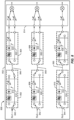
- FIG. 7 shows a detailed exemplary embodiment of a multiplex routing module (MRM) 700.
- MRM 700 is suitable for use as the multiplex modules 114 shown in FIG. 1 to efficiently route RF signals from an antenna to a demodulator for demodulation.
- the MRM 700 comprises input switch 702, output switch 704, feed-through signal path 706, filter 708, matching circuit 710, and variable gain amplifier 712.
- An RF signal received at an input terminal 714 of the input switch 702 is connected flow to the feed-through path 706 or to the filter 708. If the input switch 702 connects the input terminal 714 to the terminal 718 that is connected to the feed-through path, the input RF signal flows through the feed-through path 706 to a first terminal 724 of the output switch 704. If the input switch 702 connects the input terminal 714 to the terminal 716 that is connected to the filter 708, the input RF signal flows to the filter 708 where it is filtered and a filtered output is then input to the matching circuit 710.
- the matching circuit 710 provides matching characteristics to reduce loss or distortion of the filtered signal.
- the output of the matching circuit 710 is input to the variable gain amplifier 712 where amplification is provided to the filtered signal to generate an amplified filtered signal that flows to a second terminal 722 of the output switch 704.
- the output switch 704 has an output terminal 720 that is connected to either the first 724 or second 722 terminals to allow the RF signal to be output from the multiplex routing module 700
- the terminal 724 outputs a signal 728 that flows on the bypass path 706.
- the terminal 722 outputs a signal 726 that flows through the non-bypass path.
- the multiplex routing module 700 efficiently routes RF signals in one or more bands to a demodulator in a receiver front end.
- FIG. 8 shows a block diagram of a receiver front end 800 that comprises exemplary embodiments of the multiplex routing module 700 shown in FIG. 7 .
- the multiplex routing module 700 is suitable for use as the multiplex routing modules (MRM) 802, 804, 806, 808, 810, and 812 shown in FIG. 8 .
- MRM multiplex routing modules
- the RF signals may be received from the primary and/or diversity antennas through the antenna switch 304 shown in FIG. 3 .
- the front end 800 comprises a printed circuit board 852 onto which are mounted the multiplex routing modules 802, 804, 806, 808, 810, and 812, and a demodulator 814.
- the printed circuit board comprises signal traces that route signals between the components mounted to the printed circuit board.
- the MRM 802 receives the Rx1 signal at its input terminal 840 and selects a signal path through which the Rx1 signal will flow.
- a first signal path 816 comprises a filter, matching network, and amplifier (FMA) and a second signal path comprises a bypass signal path 818.
- FMA filter, matching network, and amplifier
- the input switch and the output switch of the MRM 802 are set to select the bypass path 818, which outputs the Rx1 signal along path 846 that is input to the input switch of the MRM 804.
- the MRM 804 also routes the signal it receives through one of a FMA path 820 or a bypass path 822.
- the input switch of the MRM 804 is set to select the FMA path 820, which outputs a filtered and amplified signal that is input to the demodulator 814.
- each of the paths 820 and 822 have a separate input into the demodulator 814, thereby facilitating separate processing of each path by the demodulator.
- the signal path selected to route the Rx1 signal is configured to provide filtering and gain adjustment by MRM 804, which is close to the demodulator. This configuration can be used when the desired signal (Rx1) is received with good signal to noise ratio (SNR) (e.g., signal power of -60dBm).
- SNR signal to noise ratio
- the MRM 806 receives the Rx2 signal at its input terminal 842 and selects a signal path through which the Rx2 signal will flow.
- a first signal path 824 comprises a filter, matching network, and amplifier (FMA) and a second signal path comprises a bypass path 826.
- FMA filter, matching network, and amplifier
- the input and output switches of the MRM 806 are set to select the FMA path 824, which outputs a filtered and amplified signal along path 848 that is input to the MRM 808.
- the MRM 808 routes the signal it receives through one of an FMA path 828 or a bypass path 830.
- the input switch of the MRM 806 is set to select the bypass path 830, which outputs the filtered and amplified Rx2 signal, which is then input to the demodulator 814.
- each of the paths 828 and 830 have a separate input into the demodulator 814, thereby facilitating separate processing of each path by the demodulator.
- the signal path selected to route the Rx2 signal is configured to provide filtering and gain adjustment by MRM 806, which is close to the antenna switch. This configuration can be used when there the desired signal (Rx2) is received with average SNR (e.g., signal power of -80dBm).
- the MRM 810 receives the Rx3 signal at its input terminal 844 and selects a signal path through which the Rx3 signal will flow.
- a first signal path 832 comprises a filter, matching network, and amplifier (FMA) and a second signal path comprises a bypass path 834.
- the input and output switches of the MRM 810 are set to select the FMA path 832, which outputs a filtered and amplified signal along signal path 850 that is input to the input switch of the MRM 812.
- the MRM 812 routes the signal it receives through one of a FMA path 836 or a bypass path 838.
- the input and output switches of the MRM 812 are set to select the FMA path 836, which provides additional filtering and amplification to the Rx3 signal.
- the output of the MRM 812 is input to the demodulator 814.
- both of the paths 836 and 838 have the same input into the demodulator 814, thereby facilitating the same processing of each path by the demodulator.
- the MRMs 810 and 812 are configured to provide filtering and gain adjustment by both of the MRM 810 and the MRM 812. This configuration can be used when there the desired signal (Rx3) is received with poor SNR (e.g., signal power of -100dBm).
- the multiplex routing modules 802, 804, 806, 808, 810 and 812 operate to receive and route RF signals to a demodulator. It should be noted that the configuration of the front end 800 is exemplary and that other configurations and/or routing paths using the same number or a different number of MRMs are possible within the scope of the exemplary embodiments.
- FIG. 9 shows a block diagram of a receiver front end 900 that comprises exemplary embodiments of the multiplex module shown in FIG. 4 and the multiplex routing module shown in FIG. 7 .
- the front end 900 comprises MRMs 902, 904, and 906 that receive RF signals Rx1, Rx2, and Rx3 from, for example, the antenna switch 304.
- Each of the MRMs 902, 904, and 906 routes their respective RF signals through FMA paths or bypass paths as selected by their input and output switches to generate outputs signals that are input to an LNA mux 908.
- the LNA mux 908 comprises a combining circuit 914, which in an exemplary embodiment is configured as the combining circuit shown in FIG. 6 .
- the LNA mux 908 sums together the outputs of the MRM 902, 904, and 906 and outputs a combined RF signal 918 that is output from the output terminal 916 and routed to an input terminal 920 of an LNA demux 910.
- the components of the front end 900 are mounted on printed circuit board 930, such that a single signal trace carries the combined RF signal 918 to the LNA demux 910.
- the LNA demux 910 is configured as the LNA demux shown in FIG. 5 .
- the LNA demux 910 distributes the received combined RF signal 918 and provides amplified outputs to mixers 924, 926, and 928 of demodulator 912.
- the outputs of the mixers are the baseband signals BB1, BB2, and BB3.
- the MRMs 902, 904, and 906 route received RF signals along a selected path (FMA or bypass) to the LNA mux 908 which combines the three signals into the combined output 918.
- This combined output can be routed across the printed circuit board 930 and each of the RF signals will flow over an identical signal path.
- the LNA demux 910 distributes the combined signal to a demodulator where the RF signals are demodulated using the appropriate LO signals to generate the desired baseband signals. Accordingly, the various multiplex modules operate to efficiently route signals in a carrier aggregation receiver.
- FIG. 10 shows an exemplary embodiment of a multiplex module apparatus 1000.
- the apparatus 1000 is suitable for use as the multiplex module 400 shown in FIG. 4 .
- the apparatus 1000 includes a first means (1002) for receiving a plurality of RF signals, which in an exemplary embodiment comprises the input terminals 402, 404, and 406.
- the apparatus 1000 also includes a second means (1004) for combining the RF signals into a combined RF signal that is output from an output terminal, which in an exemplary embodiment comprises the LNA multiplexer 310.
- the apparatus 1000 also comprises a third means (1006) for receiving the combined RF signal at an input port that is connected to the output terminal, which in an exemplary embodiment comprises the input port 434.
- the apparatus 1000 also comprises a fourth means (1008) for distributing the combined RF signal to a plurality of output ports, which in an exemplary embodiment comprises the LNA demultiplexer 314.
- CMOS complementary metal oxide semiconductor
- NMOS N-channel MOS
- PMOS P-channel MOS
- BJT bipolar junction transistor
- BiCMOS bipolar-CMOS
- SiGe silicon germanium
- GaAs gallium arsenide
- HBTs heterojunction bipolar transistors
- HEMTs high electron mobility transistors
- SOI silicon-on-insulator
- An apparatus implementing an exemplary embodiment described herein may be a stand-alone device or may be part of a larger device.
- a device may be (i) a stand-alone IC, (ii) a set of one or more ICs that may include memory ICs for storing data and/or instructions, (iii) an RFIC such as an RF receiver (RFR) or an RF transmitter/receiver (RTR), (iv) an ASIC such as a mobile station modem (MSM), (v) a module that may be embedded within other devices, (vi) a receiver, cellular phone, wireless device, handset, or mobile unit, (vii) etc.
- RFR RF receiver
- RTR RF transmitter/receiver
- MSM mobile station modem
Landscapes
- Engineering & Computer Science (AREA)
- Signal Processing (AREA)
- Computer Networks & Wireless Communication (AREA)
- Power Engineering (AREA)
- Transceivers (AREA)
- Input Circuits Of Receivers And Coupling Of Receivers And Audio Equipment (AREA)
- Amplifiers (AREA)
Applications Claiming Priority (5)
| Application Number | Priority Date | Filing Date | Title |
|---|---|---|---|
| US201461994175P | 2014-05-16 | 2014-05-16 | |
| US201461994167P | 2014-05-16 | 2014-05-16 | |
| US14/664,492 US9774485B2 (en) | 2014-05-16 | 2015-03-20 | Multiplex modules for carrier aggregation receivers |
| EP15717311.3A EP3205027B1 (fr) | 2014-05-16 | 2015-03-23 | Modules multiplex pour des récepteurs d'agrégation de porteuses |
| PCT/US2015/022055 WO2015175094A1 (fr) | 2014-05-16 | 2015-03-23 | Modules multiplex pour des récepteurs d'agrégation de porteuses |
Related Parent Applications (1)
| Application Number | Title | Priority Date | Filing Date |
|---|---|---|---|
| EP15717311.3A Division EP3205027B1 (fr) | 2014-05-16 | 2015-03-23 | Modules multiplex pour des récepteurs d'agrégation de porteuses |
Publications (2)
| Publication Number | Publication Date |
|---|---|
| EP4507258A2 true EP4507258A2 (fr) | 2025-02-12 |
| EP4507258A3 EP4507258A3 (fr) | 2025-08-20 |
Family
ID=52988418
Family Applications (2)
| Application Number | Title | Priority Date | Filing Date |
|---|---|---|---|
| EP15717311.3A Active EP3205027B1 (fr) | 2014-05-16 | 2015-03-23 | Modules multiplex pour des récepteurs d'agrégation de porteuses |
| EP24200667.4A Pending EP4507258A3 (fr) | 2014-05-16 | 2015-03-23 | Modules multiplex pour récepteurs à agrégation de porteuses |
Family Applications Before (1)
| Application Number | Title | Priority Date | Filing Date |
|---|---|---|---|
| EP15717311.3A Active EP3205027B1 (fr) | 2014-05-16 | 2015-03-23 | Modules multiplex pour des récepteurs d'agrégation de porteuses |
Country Status (3)
| Country | Link |
|---|---|
| US (2) | US9774485B2 (fr) |
| EP (2) | EP3205027B1 (fr) |
| WO (1) | WO2015175094A1 (fr) |
Families Citing this family (13)
| Publication number | Priority date | Publication date | Assignee | Title |
|---|---|---|---|---|
| US9774485B2 (en) * | 2014-05-16 | 2017-09-26 | Qualcomm Incorporated | Multiplex modules for carrier aggregation receivers |
| US10390343B2 (en) | 2014-06-23 | 2019-08-20 | Qualcomm Incorporated | Carrier aggregation diversity antenna module with integrated LNA banks |
| JP6386312B2 (ja) * | 2014-09-09 | 2018-09-05 | ルネサスエレクトロニクス株式会社 | 半導体装置 |
| US9455755B2 (en) | 2014-10-06 | 2016-09-27 | Skyworks Solutions, Inc. | Aggregate signal amplification device and method |
| US9893752B2 (en) * | 2014-10-31 | 2018-02-13 | Skyworks Solutions, Inc. | Diversity receiver front end system with variable-gain amplifiers |
| US10009201B2 (en) * | 2015-01-13 | 2018-06-26 | Samsung Electronics Co., Ltd | Receiver and wireless terminal for signal processing |
| US9793935B2 (en) * | 2015-07-02 | 2017-10-17 | Mediatek Inc. | Multi-mixer system and method for reducing interference within multi-mixer system |
| US20180062636A1 (en) * | 2016-08-26 | 2018-03-01 | Qualcomm Incorporated | Floating Gate Switch |
| US10262475B2 (en) * | 2017-01-19 | 2019-04-16 | Ford Global Technologies, Llc | Vehicle sensor health monitoring |
| WO2018168653A1 (fr) * | 2017-03-14 | 2018-09-20 | 株式会社村田製作所 | Module haute fréquence |
| JP6725059B2 (ja) | 2017-03-15 | 2020-07-15 | 株式会社村田製作所 | 高周波モジュール及び通信装置 |
| CN113055043A (zh) * | 2021-03-22 | 2021-06-29 | 西安易朴通讯技术有限公司 | 一种信号处理系统及电子设备 |
| KR20240030590A (ko) | 2022-08-31 | 2024-03-07 | 삼성전자주식회사 | 반도체 장치 |
Family Cites Families (34)
| Publication number | Priority date | Publication date | Assignee | Title |
|---|---|---|---|---|
| US6963758B2 (en) | 2000-09-29 | 2005-11-08 | Ntt Docomo, Inc. | High-sensitivity wireless receiving device and high-frequency unit used therefor |
| US7116952B2 (en) | 2003-10-09 | 2006-10-03 | Intel Corporation | Method and apparatus to provide an area efficient antenna diversity receiver |
| US7869528B2 (en) | 2003-10-31 | 2011-01-11 | Northrop Grumman Systems Corporation | Multi-carrier transceiver assembly |
| US7023272B2 (en) * | 2004-04-19 | 2006-04-04 | Texas Instruments Incorporated | Multi-band low noise amplifier system |
| US7359639B2 (en) * | 2004-05-04 | 2008-04-15 | L-3 Communications Corporation | Airborne free space optical communication apparatus and method with subcarrier multiplexing |
| JP2006135814A (ja) * | 2004-11-08 | 2006-05-25 | Fujitsu Ltd | 無線受信機 |
| KR100654459B1 (ko) * | 2005-06-30 | 2006-12-06 | 삼성전자주식회사 | 광대역 저잡음 증폭기 및 상기 증폭기를 이용한 rf 신호증폭 방법 |
| US20090108911A1 (en) | 2007-10-30 | 2009-04-30 | Rohm Co., Ltd. | Analog switch |
| KR101454487B1 (ko) * | 2008-01-04 | 2014-11-03 | 엘지전자 주식회사 | 튜너 |
| JP2009290411A (ja) * | 2008-05-28 | 2009-12-10 | Nec Electronics Corp | 低雑音受信装置 |
| WO2009157357A1 (fr) | 2008-06-25 | 2009-12-30 | 日立金属株式会社 | Circuit haute fréquence, composant haute fréquence et dispositif de communication |
| US8086197B2 (en) | 2008-11-12 | 2011-12-27 | Nxp B.V. | Multi-channel receiver architecture and reception method |
| US8045592B2 (en) | 2009-03-04 | 2011-10-25 | Laird Technologies, Inc. | Multiple antenna multiplexers, demultiplexers and antenna assemblies |
| US8976302B2 (en) * | 2009-09-30 | 2015-03-10 | Wi-Lan, Inc. | Radio frequency front end for television band receiver and spectrum sensor |
| JP2011130088A (ja) * | 2009-12-16 | 2011-06-30 | Sony Corp | 端末装置、ハンドオーバのための方法、基地局及び無線通信システム |
| US8837331B2 (en) | 2011-02-02 | 2014-09-16 | Qualcomm Incorporated | Duplexer bypass |
| EP2487800B1 (fr) | 2011-02-11 | 2013-06-19 | Alcatel Lucent | Réseaux d'antennes actives |
| US9252827B2 (en) | 2011-06-27 | 2016-02-02 | Qualcomm Incorporated | Signal splitting carrier aggregation receiver architecture |
| US12081243B2 (en) | 2011-08-16 | 2024-09-03 | Qualcomm Incorporated | Low noise amplifiers with combined outputs |
| US9154356B2 (en) * | 2012-05-25 | 2015-10-06 | Qualcomm Incorporated | Low noise amplifiers for carrier aggregation |
| US9219594B2 (en) | 2012-06-18 | 2015-12-22 | Rf Micro Devices, Inc. | Dual antenna integrated carrier aggregation front end solution |
| US9312888B2 (en) | 2012-06-29 | 2016-04-12 | Qualcomm Incorporated | Antenna interface circuits for carrier aggregation on multiple antennas |
| US9300420B2 (en) | 2012-09-11 | 2016-03-29 | Qualcomm Incorporated | Carrier aggregation receiver architecture |
| US8774068B2 (en) | 2012-10-11 | 2014-07-08 | Sony Corporation | Dual swapping switches to meet linearity demands of carrier aggregation |
| US9543903B2 (en) | 2012-10-22 | 2017-01-10 | Qualcomm Incorporated | Amplifiers with noise splitting |
| WO2015018020A1 (fr) * | 2013-08-08 | 2015-02-12 | Telefonaktiebolaget L M Ericsson (Publ) | Module amplificateur à faible bruit et procédé de mise en œuvre |
| US20150092680A1 (en) | 2013-09-30 | 2015-04-02 | Broadcom Corporation | Flexible Receiver Architecture for Multiple Component Carrier Aggregation in Down Link |
| KR101496178B1 (ko) * | 2013-11-13 | 2015-02-25 | 알에프컨트롤스 주식회사 | 차량용 통합 안테나 장치 |
| CN103780280B (zh) | 2014-02-27 | 2016-06-15 | 华为技术有限公司 | 射频通路 |
| US9374042B2 (en) * | 2014-03-27 | 2016-06-21 | Infineon Technologies Ag | System and method for a low noise amplifier |
| US9654169B2 (en) | 2014-04-22 | 2017-05-16 | Skyworks Solutions, Inc. | Apparatus and methods for multi-band radio frequency signal routing |
| US9774485B2 (en) | 2014-05-16 | 2017-09-26 | Qualcomm Incorporated | Multiplex modules for carrier aggregation receivers |
| US9473336B2 (en) | 2014-05-16 | 2016-10-18 | Qualcomm Incorporated | Radio frequency (RF) front end having multiple low noise amplifier modules |
| US10390343B2 (en) | 2014-06-23 | 2019-08-20 | Qualcomm Incorporated | Carrier aggregation diversity antenna module with integrated LNA banks |
-
2015
- 2015-03-20 US US14/664,492 patent/US9774485B2/en active Active
- 2015-03-23 EP EP15717311.3A patent/EP3205027B1/fr active Active
- 2015-03-23 WO PCT/US2015/022055 patent/WO2015175094A1/fr not_active Ceased
- 2015-03-23 EP EP24200667.4A patent/EP4507258A3/fr active Pending
-
2017
- 2017-09-25 US US15/715,006 patent/US10439858B2/en active Active
Also Published As
| Publication number | Publication date |
|---|---|
| US20180013600A1 (en) | 2018-01-11 |
| US10439858B2 (en) | 2019-10-08 |
| WO2015175094A1 (fr) | 2015-11-19 |
| US9774485B2 (en) | 2017-09-26 |
| US20150333949A1 (en) | 2015-11-19 |
| EP3205027B1 (fr) | 2024-09-18 |
| EP3205027A1 (fr) | 2017-08-16 |
| EP4507258A3 (fr) | 2025-08-20 |
Similar Documents
| Publication | Publication Date | Title |
|---|---|---|
| US10439858B2 (en) | Multiplex modules for carrier aggregation receivers | |
| CN106471744B (zh) | 具有集成lna组的载波聚合分集天线模块 | |
| JP6224293B1 (ja) | マルチバンド受信機のための2段低雑音増幅器 | |
| US9473336B2 (en) | Radio frequency (RF) front end having multiple low noise amplifier modules | |
| US20140242923A1 (en) | Shared filter for transmit and receive paths | |
| JP2026512798A (ja) | 送信(tx)受信(rx)フェーズドアレイシステム | |
| US10340860B1 (en) | Multi-mode low noise amplifier | |
| US20160218852A1 (en) | Half-duplex sawless receiver | |
| US12381603B2 (en) | Millimeter wave (MMW) downlink multiple input multiple output (MIMO) and carrier aggregation (CA) architecture |
Legal Events
| Date | Code | Title | Description |
|---|---|---|---|
| PUAI | Public reference made under article 153(3) epc to a published international application that has entered the european phase |
Free format text: ORIGINAL CODE: 0009012 |
|
| STAA | Information on the status of an ep patent application or granted ep patent |
Free format text: STATUS: REQUEST FOR EXAMINATION WAS MADE |
|
| 17P | Request for examination filed |
Effective date: 20241015 |
|
| AC | Divisional application: reference to earlier application |
Ref document number: 3205027 Country of ref document: EP Kind code of ref document: P |
|
| AK | Designated contracting states |
Kind code of ref document: A2 Designated state(s): AL AT BE BG CH CY CZ DE DK EE ES FI FR GB GR HR HU IE IS IT LI LT LU LV MC MK MT NL NO PL PT RO RS SE SI SK SM TR |
|
| REG | Reference to a national code |
Ref country code: DE Ref legal event code: R079 Free format text: PREVIOUS MAIN CLASS: H04L0027260000 Ipc: H04B0001000000 |
|
| RIC1 | Information provided on ipc code assigned before grant |
Ipc: H04L 27/26 20060101ALI20250326BHEP Ipc: H04L 5/00 20060101ALI20250326BHEP Ipc: H03F 3/24 20060101ALI20250326BHEP Ipc: H03F 3/193 20060101ALI20250326BHEP Ipc: H03F 1/22 20060101ALI20250326BHEP Ipc: H04B 1/00 20060101AFI20250326BHEP |
|
| PUAL | Search report despatched |
Free format text: ORIGINAL CODE: 0009013 |
|
| AK | Designated contracting states |
Kind code of ref document: A3 Designated state(s): AL AT BE BG CH CY CZ DE DK EE ES FI FR GB GR HR HU IE IS IT LI LT LU LV MC MK MT NL NO PL PT RO RS SE SI SK SM TR |
|
| RIC1 | Information provided on ipc code assigned before grant |
Ipc: H04B 1/00 20060101AFI20250715BHEP Ipc: H03F 1/22 20060101ALI20250715BHEP Ipc: H03F 3/193 20060101ALI20250715BHEP Ipc: H03F 3/24 20060101ALI20250715BHEP Ipc: H04L 5/00 20060101ALI20250715BHEP Ipc: H04L 27/26 20060101ALI20250715BHEP |