EP4510190A1 - Dispositifs à circuit intégré comprenant un chemin de décharge et leurs procédés de formation - Google Patents
Dispositifs à circuit intégré comprenant un chemin de décharge et leurs procédés de formation Download PDFInfo
- Publication number
- EP4510190A1 EP4510190A1 EP24177611.1A EP24177611A EP4510190A1 EP 4510190 A1 EP4510190 A1 EP 4510190A1 EP 24177611 A EP24177611 A EP 24177611A EP 4510190 A1 EP4510190 A1 EP 4510190A1
- Authority
- EP
- European Patent Office
- Prior art keywords
- diode
- source
- integrated circuit
- substrate
- region
- Prior art date
- Legal status (The legal status is an assumption and is not a legal conclusion. Google has not performed a legal analysis and makes no representation as to the accuracy of the status listed.)
- Pending
Links
Images


Classifications
-
- H—ELECTRICITY
- H10—SEMICONDUCTOR DEVICES; ELECTRIC SOLID-STATE DEVICES NOT OTHERWISE PROVIDED FOR
- H10W—GENERIC PACKAGES, INTERCONNECTIONS, CONNECTORS OR OTHER CONSTRUCTIONAL DETAILS OF DEVICES COVERED BY CLASS H10
- H10W20/00—Interconnections in chips, wafers or substrates
- H10W20/20—Interconnections within wafers or substrates, e.g. through-silicon vias [TSV]
-
- H—ELECTRICITY
- H10—SEMICONDUCTOR DEVICES; ELECTRIC SOLID-STATE DEVICES NOT OTHERWISE PROVIDED FOR
- H10D—INORGANIC ELECTRIC SEMICONDUCTOR DEVICES
- H10D89/00—Aspects of integrated devices not covered by groups H10D84/00 - H10D88/00
- H10D89/60—Integrated devices comprising arrangements for electrical or thermal protection, e.g. protection circuits against electrostatic discharge [ESD]
- H10D89/601—Integrated devices comprising arrangements for electrical or thermal protection, e.g. protection circuits against electrostatic discharge [ESD] for devices having insulated gate electrodes, e.g. for IGFETs or IGBTs
- H10D89/611—Integrated devices comprising arrangements for electrical or thermal protection, e.g. protection circuits against electrostatic discharge [ESD] for devices having insulated gate electrodes, e.g. for IGFETs or IGBTs using diodes as protective elements
-
- H—ELECTRICITY
- H10—SEMICONDUCTOR DEVICES; ELECTRIC SOLID-STATE DEVICES NOT OTHERWISE PROVIDED FOR
- H10D—INORGANIC ELECTRIC SEMICONDUCTOR DEVICES
- H10D30/00—Field-effect transistors [FET]
- H10D30/01—Manufacture or treatment
- H10D30/014—Manufacture or treatment of FETs having zero-dimensional [0D] or one-dimensional [1D] channels, e.g. quantum wire FETs, single-electron transistors [SET] or Coulomb blockade transistors
-
- H—ELECTRICITY
- H10—SEMICONDUCTOR DEVICES; ELECTRIC SOLID-STATE DEVICES NOT OTHERWISE PROVIDED FOR
- H10D—INORGANIC ELECTRIC SEMICONDUCTOR DEVICES
- H10D30/00—Field-effect transistors [FET]
- H10D30/40—FETs having zero-dimensional [0D], one-dimensional [1D] or two-dimensional [2D] charge carrier gas channels
- H10D30/43—FETs having zero-dimensional [0D], one-dimensional [1D] or two-dimensional [2D] charge carrier gas channels having one-dimensional [1D] charge carrier gas channels, e.g. quantum wire FETs or transistors having 1D quantum-confined channels
-
- H—ELECTRICITY
- H10—SEMICONDUCTOR DEVICES; ELECTRIC SOLID-STATE DEVICES NOT OTHERWISE PROVIDED FOR
- H10D—INORGANIC ELECTRIC SEMICONDUCTOR DEVICES
- H10D30/00—Field-effect transistors [FET]
- H10D30/60—Insulated-gate field-effect transistors [IGFET]
- H10D30/67—Thin-film transistors [TFT]
- H10D30/6729—Thin-film transistors [TFT] characterised by the electrodes
- H10D30/673—Thin-film transistors [TFT] characterised by the electrodes characterised by the shapes, relative sizes or dispositions of the gate electrodes
- H10D30/6735—Thin-film transistors [TFT] characterised by the electrodes characterised by the shapes, relative sizes or dispositions of the gate electrodes having gates fully surrounding the channels, e.g. gate-all-around
-
- H—ELECTRICITY
- H10—SEMICONDUCTOR DEVICES; ELECTRIC SOLID-STATE DEVICES NOT OTHERWISE PROVIDED FOR
- H10D—INORGANIC ELECTRIC SEMICONDUCTOR DEVICES
- H10D30/00—Field-effect transistors [FET]
- H10D30/60—Insulated-gate field-effect transistors [IGFET]
- H10D30/67—Thin-film transistors [TFT]
- H10D30/6757—Thin-film transistors [TFT] characterised by the structure of the channel, e.g. transverse or longitudinal shape or doping profile
-
- H—ELECTRICITY
- H10—SEMICONDUCTOR DEVICES; ELECTRIC SOLID-STATE DEVICES NOT OTHERWISE PROVIDED FOR
- H10D—INORGANIC ELECTRIC SEMICONDUCTOR DEVICES
- H10D62/00—Semiconductor bodies, or regions thereof, of devices having potential barriers
- H10D62/10—Shapes, relative sizes or dispositions of the regions of the semiconductor bodies; Shapes of the semiconductor bodies
- H10D62/117—Shapes of semiconductor bodies
- H10D62/118—Nanostructure semiconductor bodies
- H10D62/119—Nanowire, nanosheet or nanotube semiconductor bodies
- H10D62/121—Nanowire, nanosheet or nanotube semiconductor bodies oriented parallel to substrates
-
- H—ELECTRICITY
- H10—SEMICONDUCTOR DEVICES; ELECTRIC SOLID-STATE DEVICES NOT OTHERWISE PROVIDED FOR
- H10D—INORGANIC ELECTRIC SEMICONDUCTOR DEVICES
- H10D84/00—Integrated devices formed in or on semiconductor substrates that comprise only semiconducting layers, e.g. on Si wafers or on GaAs-on-Si wafers
- H10D84/01—Manufacture or treatment
- H10D84/0123—Integrating together multiple components covered by H10D12/00 or H10D30/00, e.g. integrating multiple IGBTs
- H10D84/0126—Integrating together multiple components covered by H10D12/00 or H10D30/00, e.g. integrating multiple IGBTs the components including insulated gates, e.g. IGFETs
- H10D84/0165—Integrating together multiple components covered by H10D12/00 or H10D30/00, e.g. integrating multiple IGBTs the components including insulated gates, e.g. IGFETs the components including complementary IGFETs, e.g. CMOS devices
- H10D84/0167—Manufacturing their channels
-
- H—ELECTRICITY
- H10—SEMICONDUCTOR DEVICES; ELECTRIC SOLID-STATE DEVICES NOT OTHERWISE PROVIDED FOR
- H10D—INORGANIC ELECTRIC SEMICONDUCTOR DEVICES
- H10D84/00—Integrated devices formed in or on semiconductor substrates that comprise only semiconducting layers, e.g. on Si wafers or on GaAs-on-Si wafers
- H10D84/01—Manufacture or treatment
- H10D84/0123—Integrating together multiple components covered by H10D12/00 or H10D30/00, e.g. integrating multiple IGBTs
- H10D84/0126—Integrating together multiple components covered by H10D12/00 or H10D30/00, e.g. integrating multiple IGBTs the components including insulated gates, e.g. IGFETs
- H10D84/0165—Integrating together multiple components covered by H10D12/00 or H10D30/00, e.g. integrating multiple IGBTs the components including insulated gates, e.g. IGFETs the components including complementary IGFETs, e.g. CMOS devices
- H10D84/017—Manufacturing their source or drain regions, e.g. silicided source or drain regions
-
- H—ELECTRICITY
- H10—SEMICONDUCTOR DEVICES; ELECTRIC SOLID-STATE DEVICES NOT OTHERWISE PROVIDED FOR
- H10D—INORGANIC ELECTRIC SEMICONDUCTOR DEVICES
- H10D84/00—Integrated devices formed in or on semiconductor substrates that comprise only semiconducting layers, e.g. on Si wafers or on GaAs-on-Si wafers
- H10D84/01—Manufacture or treatment
- H10D84/0123—Integrating together multiple components covered by H10D12/00 or H10D30/00, e.g. integrating multiple IGBTs
- H10D84/0126—Integrating together multiple components covered by H10D12/00 or H10D30/00, e.g. integrating multiple IGBTs the components including insulated gates, e.g. IGFETs
- H10D84/0165—Integrating together multiple components covered by H10D12/00 or H10D30/00, e.g. integrating multiple IGBTs the components including insulated gates, e.g. IGFETs the components including complementary IGFETs, e.g. CMOS devices
- H10D84/0172—Manufacturing their gate conductors
- H10D84/0177—Manufacturing their gate conductors the gate conductors having different materials or different implants
-
- H—ELECTRICITY
- H10—SEMICONDUCTOR DEVICES; ELECTRIC SOLID-STATE DEVICES NOT OTHERWISE PROVIDED FOR
- H10D—INORGANIC ELECTRIC SEMICONDUCTOR DEVICES
- H10D84/00—Integrated devices formed in or on semiconductor substrates that comprise only semiconducting layers, e.g. on Si wafers or on GaAs-on-Si wafers
- H10D84/01—Manufacture or treatment
- H10D84/0123—Integrating together multiple components covered by H10D12/00 or H10D30/00, e.g. integrating multiple IGBTs
- H10D84/0126—Integrating together multiple components covered by H10D12/00 or H10D30/00, e.g. integrating multiple IGBTs the components including insulated gates, e.g. IGFETs
- H10D84/0165—Integrating together multiple components covered by H10D12/00 or H10D30/00, e.g. integrating multiple IGBTs the components including insulated gates, e.g. IGFETs the components including complementary IGFETs, e.g. CMOS devices
- H10D84/0186—Manufacturing their interconnections or electrodes, e.g. source or drain electrodes
-
- H—ELECTRICITY
- H10—SEMICONDUCTOR DEVICES; ELECTRIC SOLID-STATE DEVICES NOT OTHERWISE PROVIDED FOR
- H10D—INORGANIC ELECTRIC SEMICONDUCTOR DEVICES
- H10D84/00—Integrated devices formed in or on semiconductor substrates that comprise only semiconducting layers, e.g. on Si wafers or on GaAs-on-Si wafers
- H10D84/01—Manufacture or treatment
- H10D84/02—Manufacture or treatment characterised by using material-based technologies
- H10D84/03—Manufacture or treatment characterised by using material-based technologies using Group IV technology, e.g. silicon technology or silicon-carbide [SiC] technology
- H10D84/038—Manufacture or treatment characterised by using material-based technologies using Group IV technology, e.g. silicon technology or silicon-carbide [SiC] technology using silicon technology, e.g. SiGe
-
- H—ELECTRICITY
- H10—SEMICONDUCTOR DEVICES; ELECTRIC SOLID-STATE DEVICES NOT OTHERWISE PROVIDED FOR
- H10D—INORGANIC ELECTRIC SEMICONDUCTOR DEVICES
- H10D84/00—Integrated devices formed in or on semiconductor substrates that comprise only semiconducting layers, e.g. on Si wafers or on GaAs-on-Si wafers
- H10D84/80—Integrated devices formed in or on semiconductor substrates that comprise only semiconducting layers, e.g. on Si wafers or on GaAs-on-Si wafers characterised by the integration of at least one component covered by groups H10D12/00 or H10D30/00, e.g. integration of IGFETs
- H10D84/811—Combinations of field-effect devices and one or more diodes, capacitors or resistors
-
- H—ELECTRICITY
- H10—SEMICONDUCTOR DEVICES; ELECTRIC SOLID-STATE DEVICES NOT OTHERWISE PROVIDED FOR
- H10D—INORGANIC ELECTRIC SEMICONDUCTOR DEVICES
- H10D84/00—Integrated devices formed in or on semiconductor substrates that comprise only semiconducting layers, e.g. on Si wafers or on GaAs-on-Si wafers
- H10D84/80—Integrated devices formed in or on semiconductor substrates that comprise only semiconducting layers, e.g. on Si wafers or on GaAs-on-Si wafers characterised by the integration of at least one component covered by groups H10D12/00 or H10D30/00, e.g. integration of IGFETs
- H10D84/82—Integrated devices formed in or on semiconductor substrates that comprise only semiconducting layers, e.g. on Si wafers or on GaAs-on-Si wafers characterised by the integration of at least one component covered by groups H10D12/00 or H10D30/00, e.g. integration of IGFETs of only field-effect components
- H10D84/83—Integrated devices formed in or on semiconductor substrates that comprise only semiconducting layers, e.g. on Si wafers or on GaAs-on-Si wafers characterised by the integration of at least one component covered by groups H10D12/00 or H10D30/00, e.g. integration of IGFETs of only field-effect components of only insulated-gate FETs [IGFET]
- H10D84/85—Complementary IGFETs, e.g. CMOS
- H10D84/853—Complementary IGFETs, e.g. CMOS comprising FinFETs
-
- H—ELECTRICITY
- H10—SEMICONDUCTOR DEVICES; ELECTRIC SOLID-STATE DEVICES NOT OTHERWISE PROVIDED FOR
- H10D—INORGANIC ELECTRIC SEMICONDUCTOR DEVICES
- H10D88/00—Three-dimensional [3D] integrated devices
-
- H—ELECTRICITY
- H10—SEMICONDUCTOR DEVICES; ELECTRIC SOLID-STATE DEVICES NOT OTHERWISE PROVIDED FOR
- H10D—INORGANIC ELECTRIC SEMICONDUCTOR DEVICES
- H10D89/00—Aspects of integrated devices not covered by groups H10D84/00 - H10D88/00
- H10D89/60—Integrated devices comprising arrangements for electrical or thermal protection, e.g. protection circuits against electrostatic discharge [ESD]
- H10D89/601—Integrated devices comprising arrangements for electrical or thermal protection, e.g. protection circuits against electrostatic discharge [ESD] for devices having insulated gate electrodes, e.g. for IGFETs or IGBTs
- H10D89/931—Integrated devices comprising arrangements for electrical or thermal protection, e.g. protection circuits against electrostatic discharge [ESD] for devices having insulated gate electrodes, e.g. for IGFETs or IGBTs characterised by the dispositions of the protective arrangements
-
- H—ELECTRICITY
- H10—SEMICONDUCTOR DEVICES; ELECTRIC SOLID-STATE DEVICES NOT OTHERWISE PROVIDED FOR
- H10D—INORGANIC ELECTRIC SEMICONDUCTOR DEVICES
- H10D8/00—Diodes
Definitions
- the present disclosure generally relates to the field of integrated circuit devices and, more particularly, to three-dimensional integrated circuit devices that include stacked transistors.
- an integrated circuit device may include a substrate; a first transistor structure on the substrate; a second transistor structure stacked in a vertical direction on the first transistor structure; an isolation layer between the first transistor structure and the second transistor structure in the vertical direction; and a diode structure on the substrate and adjacent to the first transistor structure in a horizontal direction.
- the diode structure may be part of a discharging path between a gate electrode of the second transistor structure and the substrate. The discharging path may extend through the isolation layer.
- an integrated circuit device may include a substrate, and a stacked structure.
- the stacked structure may include a first transistor structure on the substrate and comprising a first source/drain region having a first conductivity type; and a second transistor structure stacked in a vertical direction on the first transistor structure, the second transistor structure comprising a second source/drain region having a second conductivity type that is opposite from the first conductivity type.
- the integrated circuit device may include an isolation layer between the first transistor structure and the second transistor structure in the vertical direction; and the integrated circuit device may include a discharging path between a gate electrode of the second transistor structure and the substrate. The discharging path may extend through the isolation layer.
- the discharging path may include a diode structure, and at least a portion of the diode structure may be below an upper surface of the substrate.
- a method of forming an integrated circuit device may include: forming a stacked structure on a substrate, the stacked structure comprising lower channel layers, upper channel layers, and an isolation layer between the lower and upper channel layers; forming source/drain regions in the stacked structure, the source/drain regions comprising lower source/drain regions and upper source/drain regions; forming a diode structure in the stacked structure; forming gate structures in the stacked structure, the gate structures comprising lower gate structures and upper gate structures; and forming a discharging path between an upper gate structure and the substrate, the discharging path including the diode structure and extending through the isolation layer.
- FIG. 1 is a layout of an integrated circuit device according to some embodiments.
- FIGS. 2A and 2B are cross-sectional views of an integrated circuit device 1 taken along the line A-A' and the line B-B', respectively, in FIG. 1 according to some embodiments.
- FIG. 1 is a layout of an integrated circuit device according to some embodiments.
- FIGS. 2A and 2B are cross-sectional views of an integrated circuit device 1 taken along the line A-A' and the line B-B', respectively, in FIG. 1 according to some embodiments.
- FIG. 1 is a layout of an integrated circuit device according to some embodiments.
- FIGS. 2A and 2B are cross-sectional views of an integrated circuit device 1 taken along the line A-A' and the line B-B', respectively, in FIG. 1 according to some embodiments.
- the first integrated circuit device 1 may include a stacked structure 1S provided on a substrate 112.
- a plurality of stacked structures 1S may be provided.
- Each stacked structure 1S may include an upper transistor structure 200 (which may also be referred to as a second transistor structure) and a lower transistor structure 100 (which may also be referred to as a first transistor structure) that is provided between the substrate 112 and the upper transistor structure 200.
- the upper transistor structure 200 may be stacked on the lower transistor structure 100, which may be on the substrate 112.
- the substrate 112 may include a lower surface 112a and an upper surface 112b opposite the lower surface 112a.
- the lower surface 112a and the upper surface 112b may be parallel to each other.
- a "lower” component on the substrate 112 may refer to a first component that is closer to a lower surface 112a of the substrate 112 than a second component on the substrate 112.
- an "upper” component may refer to a second component which may on the substrate 112 and farther from the lower surface 112a of the substrate 112 than the first component.
- a semiconductor region 114 (e.g., a first semiconductor region 114a, a second semiconductor region 114b) may be provided on the substrate 112.
- the semiconductor region 114 may extend in a first direction D1 (also referred to as a first horizontal direction) and may be spaced apart from other semiconductor regions 114 in a second direction D2 (also referred to as a second horizontal direction).
- a first direction D1 also referred to as a first horizontal direction
- D2 also referred to as a second horizontal direction
- an element e.g., an "element A” said to extend in a direction (e.g., "direction X"), or similar language, may mean that the element extends longitudinally in the direction.
- the first direction D1 may be perpendicular to the second direction D2.
- the semiconductor region 114 may protrude from the upper surface 112b of the substrate 112 in a third direction D3 (also referred to as a vertical direction).
- the third direction D3 may be perpendicular to the first direction D1 and the second direction D2.
- the third direction D3 may be perpendicular to the lower surface 112a and the upper surface 112b of the substrate 112.
- the substrate 112 may include one or more semiconductor materials, for example, Si, Ge, SiGe, GaP, GaAs, SiC, SiGeC and/or InP or may include insulating material, for example, silicon oxide, silicon oxynitride, silicon nitride, silicon carbonitride, silicon boron nitride and/or a low-k material.
- the substrate 112 may be a bulk substrate (e.g., a bulk silicon substrate) or a semiconductor on insulator (SOI) substrate.
- the substrate 112 may be a silicon wafer or may be an insulating layer.
- the semiconductor region 114 may be, for example, a portion of the substrate 112 or may be a layer formed using the substrate 112 as a seed layer through, for example, an epitaxial growth process.
- the semiconductor region 114 may include semiconductor material(s), for example, Si, Ge, SiGe, GaP, GaAs, SiC, SiGeC and/or InP.
- a trench isolation layer may be provided on the substrate 112. Semiconductor regions 114 adjacent to each other may be separated from each other by a portion of the trench isolation layer.
- the trench isolation layer may include an insulating material(s) (e.g., silicon oxide, silicon oxynitride, silicon nitride, silicon carbonitride and/or a low-k material).
- the low-k material may include, for example, fluorine-doped silicon oxide, organosilicate glass, carbon-doped oxide, porous silicon dioxide, porous organosilicate glass, spin-on organic polymeric dielectrics and/or spin-on silicon based polymeric dielectric.
- a bottom insulating layer (not shown) may be formed between the substrate 112 and at least portions of the lower transistor structure 100.
- the lower transistor structure 100 may include lower channel regions 120 that may be stacked on the substrate 112 in the third direction D3 and may overlap each other in the third direction D3.
- a first element and a second element may be said to overlap each other in a given direction if, as an example, at least one (straight) line can be drawn in the given direction that intersects both the first element and the second element.
- the lower channel regions 120 may be stacked on the semiconductor region (e.g., the semiconductor region 114).
- the lower channel regions 120 may include opposing side surfaces that are spaced apart from each other in the first direction D1, and the lower transistor structure 100 may include a pair of lower source/drain regions 140 respectively on those opposing side surfaces of the lower channel regions 120.
- the pair of lower source/drain regions 140 may contact those opposing side surfaces of the lower channel regions 120, respectively.
- the lower transistor structure 100 may also include a lower gate structure 130 that may include a lower gate insulator 131 and a lower gate electrode 132.
- the lower gate electrode 132 may extend in the second direction D2 and may traverse one or more semiconductor regions 114.
- a portion of the lower channel regions 120 may surrounded by the lower gate electrode 132, and the lower gate insulator 131 may separate the lower channel regions 120 from the lower gate electrode 132.
- the lower channel regions 120 may extend through the lower gate electrode 124b in the first direction D1 and may contact the lower gate insulator 131.
- the upper transistor structure 200 may include upper channel regions 220 that may be stacked on the substrate 112 in the third direction D3 and may overlap each other in the third direction D3.
- the upper channel regions 220 may also overlap the lower channel regions 120 in the third direction D3.
- the upper channel regions 220 may include opposing side surfaces that are spaced apart from each other in the first direction D1, and the upper transistor structure 200 may include a pair of upper source/drain regions 240 respectively on those opposing side surfaces of the upper channel regions 220.
- the pair of upper source/drain regions 240 may contact those opposing side surfaces of the upper channel regions 220, respectively.
- the upper transistor structure 200 may also include an upper gate structure 230 that may include an upper gate insulator 231 and an upper gate electrode 232.
- the upper gate electrode 232 may extend in the second direction D2 and may traverse the semiconductor region 114.
- a portion of the upper channel regions 220 may be surrounded by the upper gate electrode 232, and the upper gate insulator 231 may separate the upper channel regions 220 from the upper gate electrode 232.
- the upper channel regions 220 may extend through the upper gate electrode 232 in the first direction D1 and may contact the upper gate insulator 231.
- the lower channel regions 120 and upper channel regions 220 may include, for example, semiconductor material(s) (e.g., Si, Ge, SiGe, GaP, GaAs, SiC, SiGeC and/or InP).
- the lower channel regions 120 may include a material different from the upper channel regions 220.
- each of the lower channel regions 120 and the upper channel regions 220 may be a nanosheet that may have a thickness in a range of from 1 nm to 100 nm in the third direction D3 or may be a nanowire that may have a circular cross-section with a diameter in a range of from 1 nm to 100 nm.
- the lower gate insulator 131 and the upper gate insulators 231 may include, for example, a silicon oxide layer and/or a high-k material layer.
- the high-k material layer may include, for example, Al 2 O 3 , HfO 2 , ZrO 2 , HfZrO 4 , TiO 2 , Sc 2 O 3 Y 2 O 3 , La 2 O 3 , Lu 2 O 3 , Nb 2 O 5 and/or Ta 2 O 5 .
- the lower gate insulator 131 and upper gate insulator 231 may be a gate dielectric layer.
- the lower gate electrodes 132 and the upper gate electrodes 232 may include, for example, a metallic layer that includes, for example W, Al, Cu, Mo, Co and/or Ru and may additionally include work function layer(s) (e.g., a TiN layer, a TaN layer, a TiAl layer, a TiC layer, a TiAlC layer, a TiAlN layer and/or a WN layer).
- a metallic layer that includes, for example W, Al, Cu, Mo, Co and/or Ru
- work function layer(s) e.g., a TiN layer, a TaN layer, a TiAl layer, a TiC layer, a TiAlC layer, a TiAlN layer and/or a WN layer.
- a lower insulating spacer e.g., a lower gate spacer or a lower inner gate spacer (not shown) may be provided between and separate the lower gate structure 130 and the lower source/drain region 140.
- an upper insulating spacer e.g., an upper gate spacer or an upper inner gate spacer (not shown) may be provided between and separate the upper gate structure 230 and an upper source/drain region 240.
- Each of the lower insulating spacer and the upper insulating spacer may include, for example, silicon oxide, silicon oxynitride, silicon nitride, silicon carbonitride and/or a low-k material.
- the lower transistor structure 100 and the upper transistor structure 200 may have different conductivity types, and the stacked structure 1S including the lower transistor structure 100 and the upper transistor structure 200 may be a complementary metal-oxide-semiconductor (CMOS).
- CMOS complementary metal-oxide-semiconductor
- the lower source/drain regions 140 of the lower transistor structure 100 may have a first conductivity type (e.g., P-type conductivity)
- the upper source/drain regions 240 of the upper transistor structure 200 may have a second conductivity type (e.g., N-type conductivity) that is opposite to the first conductivity type.
- the first integrated circuit device 1 may further include a middle isolation layer 300 (which may also be referred to as isolation layer) that is between the lower transistor structure 100 and the upper transistor structure 200 in the third direction D3.
- the middle isolation layer 300 may provide isolation between the lower transistor structure 100 and the upper transistor structure 200.
- the middle isolation layer 300 is shown as a single layer, the present disclosure is not limited thereto.
- an intergate isolation layer may be provided between the lower gate structure 130 and the upper gate structure 230, and an inter-source/drain isolation layer may be provided between a lower source/drain region 140 of the lower transistor structure 100 and an upper source/drain region 240 of the upper transistor structure 200.
- the intergate isolation layer and the inter-source/drain isolation layer may be provided at substantially an equal distance from a upper surface 112b of the substrate 112.
- the first integrated circuit device 1 may further include additional insulating layers, such as an insulating layer 320.
- the additional insulating layers may be on one or more sides of the first integrated circuit device 1, or the lower transistor structure 100 or the upper transistor structure 200 thereof, e.g., in a first direction D1, second direction D2, and/or third direction D3.
- Gate contacts 330 may be arranged to provide electrical connections to the gate electrodes 132/232.
- Source/drain contacts 340 may be arranged to provide electrical connections to the source/drain regions 140/240. Although the source/drain contacts 340 are shown as being connected to the upper transistor structure 200 in FIG. 2A , the present disclosure is not limited thereto, and source/drain contacts 340 may be connected with the lower source/drain regions 140 of the lower transistor structure 100. Similarly, although the gate contacts 330 are shown as being connected to the upper transistor structure 200 in FIG. 2A , the present disclosure is not limited thereto, and gate contacts 330 may be connected with the lower gate electrodes 132 of the lower transistor structure 100.
- one or more metal layers including a first metal layer 360, may be provided above the source/drain contacts 340 and gate contacts 330.
- the one or more metal layers may be back end of line (BEOL) metal layers.
- Metal lines provided in the one or more metal layers may be electrically coupled to the source/drain contacts 340 and/or gate contacts 330.
- Plasma using processes may be used at one or more steps.
- Plasma induced charges may be captured on the one or more metal lines, and the plasma induced charges may flow into gate dielectric layers (such as lower gate insulator 131 or upper gate insulator 231), resulting in potential breakdown of a gate dielectric layer.
- This accumulation of charge may be particularly problematic for the upper transistor structure 200, as the presence of the middle isolation layer 300 may act as a barrier for charges that accumulate in the upper gate structure 230 from discharging into e.g., the substrate 112.
- a discharging path may be provided between the substrate 112 and the upper transistor structure 200.
- the discharging path may include a diode structure DS.
- the diode structure DS may be located adjacent to the stacked structure 1S in a horizontal direction (e.g., the second direction D2).
- the diode structure DS may include a first semiconductor region 106 and a second semiconductor region 108, which may be a first diode region 106 and a second diode region 108, respectively.
- the first diode region 106 may be a lower diode region may have a conductivity type that is the same as the conductivity type of the lower source/drain region 140 (e.g., the first conductivity type).
- the second diode region 108 may be an upper diode region and may have a conductivity type that is the same as the conductivity type of the upper source/drain regions 240 (e.g., the second conductivity type).
- the first diode region 106 and the second diode region 108 may directly contact one another and form a junction (e.g., a P-N junction) therebetween.
- the first diode region 106 and the second diode region 108 may be vertically stacked, where the second diode region 108 is on the first diode region 106 in the third (vertical) direction D3.
- the first diode region 106 and the second diode region 108 are shown to be wider in the second direction D2 than the lower source/drain regions 140 and the upper source/drain regions 240, but this is merely one example and the present disclosure is not limited thereto.
- the first diode region 106 and/or the second diode region 108 may have the same dimensions in one or more directions as the lower source/drain region 140 and the upper source/drain regions 240.
- the first diode region 106 and/or the second diode region 108 may have different dimensions in one or more directions than one or both of the lower source/drain regions 140 and the upper source/drain regions 240. At least one of the first diode region 106 and the second diode region 108 (or a portion thereof) may horizontally overlap with the lower source/drain region 140, e.g., in the second direction D2.
- an upper surface of the lower source/drain region 140 of the lower transistor structure 100 and an upper surface of the second diode region 108 of the diode structure DS may be an equal distance from the substrate 112.
- at least a lower surface 106a of the first diode region 106 may be below an upper surface 112b of the substrate 112.
- the entirety of the first diode region106 may be below the upper surface 112b of the substrate 112.
- the first diode region 106 may be a region or portion of the substrate 112 that is doped or receives dopants to provide a selected conductivity type therein.
- a region or portion of the substrate 112 in which the diode structure DS is located may be provided with P-type dopants (e.g., boron (B), arsenic (As), phosphorous (P), and/or others).
- P-type dopants e.g., boron (B), arsenic (As), phosphorous (P), and/or others.
- the second diode region 108 may be formed at a same time as the lower source/drain region 140.
- the middle isolation layer 300 may be above the diode structure DS.
- a third semiconductor region 208 may be formed above the second semiconductor region/second diode region 108 and the first semiconductor region/first diode region 106.
- the third semiconductor region 208 may be a dummy source/drain region, and may be formed at the same time as the upper source/drain regions 240.
- a discharge contact 370 may be formed which may have at least a lower surface that contacts (e.g., directly contacts) the second diode region 108.
- the discharge contact 370 may penetrate or extend through the middle isolation layer 300.
- the discharge contact 370 may be in electrical contact with the first metal layer 360 through a discharge via 372.
- the discharge via 372 may directly contact an upper surface or upper portion of the discharge contact 370.
- a gate via 332 may be formed which may electrically connect the first metal layer 360 with a gate contact 330.
- one or more of the discharge via 372 and the gate via 332 are optional and a bottom or lower surface of the first metal layer 360 may directly contact upper surfaces of the discharge contact 370 and/or the gate contact 330.
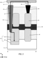
- FIG. 3 is a schematic diagram showing that a discharging path DP between the upper transistor structure 200 of the stacked structure 1S and the substrate 112 may be formed, using at least one metal layer (e.g., the first metal layer 360), which may be a BEOL metal layer and using a diode structure DS that is formed adjacent to the stacked structure 1S.
- FIG. 4 is a circuit diagram of some components of the integrated circuit device of FIG. 3 according to some embodiments.
- the discharging path DP may be an electrical path from the upper gate structure 230 or the upper gate electrode 232 of the upper transistor structure 200 (which may be a testing transistor) to the substrate 112, and the discharging path DP may include the gate contact 330, the gate via 332, a metal line formed in the first metal layer 360, the discharge via 372, the discharge contact 370, and the diode structure DS (the second diode region 108 and the first diode region 106).
- the discharging path DP may extend through the middle isolation layer 300.
- metal layer 360 is described as the first metal layer 360, it is to be understood that any metal layer (e.g., M1, M2) on a common side of the substrate 112 with the stacked structure 1S may be used as in the discharging path DP.
- metal layer e.g., M1, M2
- the discharging path DP may provide a path for charges (e.g., plasma induced charges) that may be captured in the upper transistor structure 200 to dissipate or discharge, rather than accumulate in portions of the upper transistor structure 200, such as the upper channel regions 220, which may be floating regions. This may improve the performance and/or reliability of the integrated circuit device 1, for example because the upper gate insulator 231 may not be degraded or may not experience breakdown due to accumulated plasma induced charges.
- charges e.g., plasma induced charges
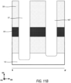
- FIG. 5 is a cross-sectional view of an integrated circuit device 2 taken along the line B-B' in FIG. 1 according to some embodiments.
- the integrated circuit device 2 may be similar to the integrated circuit 1 of FIGS. 1 , 2A , and 2B , with the primary difference being that the third semiconductor region 208 (the dummy source/drain region) may not be formed.
- FIG. 5 also shows that in some embodiments, the lower surface 108a of the second diode region 108 may be below an upper surface 112b of the substrate 112.
- the integrated circuit device 1 of FIGS. 1 , 2A , and 2B may be modified accordingly.
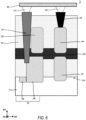
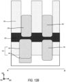
- FIG. 6 is a cross-sectional view of an integrated circuit device 3 taken along the line B-B' in FIG. 1 according to some embodiments.
- the integrated circuit device 3 may be similar to the integrated circuit 1 of FIGS. 1 , 2A , and 2B , with the primary difference being that the second diode region 108 and the first diode region 106 may not be vertically stacked, with the second diode region 108 adjacent to the first diode region 106 in a horizontal direction (e.g., the second direction D2).
- a height in the third direction D3 of the second diode region 108 may be greater than a height in the third direction D3 of the first diode region 106.
- a height in the third direction D3 of the second diode region 108 may be greater than a height in the third direction D3 of the lower source/drain region 140.
- the second diode region 108 is shown as a continuous region in FIG. 6 , the present disclosure is not limited thereto, and in some embodiments one or more sub-regions or layers may be formed which together constitute the second diode region 108. The same may be said of any of the layers or regions provided herein, unless otherwise stated.
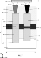
- FIG. 7 is a cross-sectional view of an integrated circuit device 4 taken along the line B-B' in FIG. 1 according to some embodiments.
- the integrated circuit device 4 may be similar to the integrated circuit device 1 with a primary difference being that a semiconductor layer 52 is provided between the third semiconductor region 208 and the second diode region 108 and contacts both the third semiconductor region 208 and the second diode region 108.
- the third semiconductor region 208 may be a third diode region 208.
- the third semiconductor region 208, the semiconductor layer 52 and the second diode region 108 may collectively form a single diode region, and together with the first diode region 106 may collectively form a single diode.
- the third semiconductor region 208, the semiconductor layer 52, and the second diode region 108 may have a common conductivity type (which may be the same conductivity type as the upper source/drain regions 240 of the upper transistor structure 200).
- FIG. 8 is a cross-sectional view of an integrated circuit device taken along the line B-B' in FIG. 1 according to some embodiments.
- the integrated circuit device 5 may be similar to the integrated circuit device 1 with a primary difference being that the diode structure DS may be formed from the first diode region 106 and the third semiconductor region 208, which may directly contact each other.
- the first diode region 106 may have the same conductivity type as the lower source/drain region 140, and the first diode region 106 and the lower source/drain region 140 may be formed at the same time and via the same process.
- the third semiconductor region 208 may have the same conductivity type as the upper source/drain regions 240, and the third semiconductor region 208 and the upper source/drain regions 240 may be formed at the same time and via the same process.
- the third semiconductor region 208 and the first diode region 106 may collectively form a single diode.
- the second diode region 108 may not be formed.
- FIG. 9 is a flowchart showing operations in a method of forming an integrated circuit device according to some embodiments.
- FIGS. 10 , 11A , 12A , and 13 are intermediate cross-sectional views taken along line A-A' of FIG. 1
- FIGS. 11B , 12B , 14 , 15 , and 16 are intermediate cross-sectional views taken along line B-B' of FIG. 1 .
- a stack structure STU (which may also be referred to as a stacked structure) may be formed by one or more of various processes (block 902 of FIG. 9 ).
- an upper stack portion UST may be formed by forming upper channel layers 220, upper sacrificial layers 1230 that are alternately stacked with the upper channel layers 220 and an insulator layer 1300 (which may also be referred to as an insolation layer) on an upper substrate 1112 and then performing an ion implantation process to form a separation layer 1111.
- the ion implantation process may implant ions (e.g., hydrogen ions) into a portion of the upper substrate 1112, and thus the separation layer 1111 may include those implanted ions.
- the upper stack portion UST may be formed by forming the separation layer 1111 through, for example, a deposition process on the upper substrate 1112, and then the upper channel layers 220, the upper sacrificial layers 1230 and the insulator layer 1300 may be formed on the separation layer 1111.
- the separation layer 1111 may include, for example, SiN, SiBCN, SiOCN, SiBN, SiCN, SiO and/or SiON.
- a lower stack portion LST may be formed and may include a lower substrate 112, and lower channel layers 120 and lower sacrificial layers 1130 stacked alternately with the lower channel layers 120 on the lower substrate 112.
- the lower sacrificial layers 1130 and the upper sacrificial layers 1230 may include a material having an etch selectivity with respect to the lower and upper channel layers 120 and 220.
- the lower and upper sacrificial layers 1130 and 1230 may include, for example, semiconductor material(s) (e.g., Si, Ge, SiGe, GaP, GaAs, SiC, SiGeC and/or InP).
- the lower and upper sacrificial layers 1130 and 1230 may include a SiGe layer.
- An upper surface (1300a) of the insulator layer 1300 may be stacked on the uppermost layer 120/1130 of the lower stack portion LST.
- the upper substrate 1112 and the separation layer 1111 may then be removed, thereby forming the stack structure STU.
- the separation layer 1111 may be removed by performing an annealing process to split the separation layer 1111 from the upper channel layers 220.
- a dry etching process and/or a Chemical Mechanical Polishing (CMP) process may be performed to remove the upper substrate 1112 and the separation layer 1111, and the separation layer 1111 may be used as an etch stop layer while removing the upper substrate 1112.
- CMP Chemical Mechanical Polishing
- the lower stack portion LST may also include an insulator layer similar to the insulator layer 1300 of the upper stack portion UST, and the upper stack portion UST may be stacked on the insulator layer of the lower stack portion LST.
- the lower stack portion LST may include an insulator layer similar to the insulator layer 1300 of the upper stack portion UST, and the insulator layer 1300 of the upper stack portion UST may be omitted, and the upper stack portion UST may be stacked on the insulator layer of the lower stack portion LST.
- the stack structure STU may be formed by providing a lower substrate 112, and then alternately stacking the lower channel layers 120 and the lower sacrificial layers 1130 on the lower substrate 112.
- the insulator layer 1300 may then be formed on the stack of lower channel layers 120 and the lower sacrificial layers 1130.
- Upper sacrificial layers 1230 and upper channel layers 220 may be alternately stacked on the insulator layer 1300, which may become the middle isolation layer 300.
- the upper substrate 1112 and the separation layer 1111 may not be used in the formation of the stack structure STU.
- source/drain trenches 140T and diode trenches DT may be formed in the stack structure STU.
- a mask layer (not shown) may be formed and the stack structure STU may be etched using the mask layer as an etch mask until the substrate 112 is exposed, thereby forming semiconductor regions 114. The mask layer may then be removed, and an insulating layer 320 may be formed on remaining portions of the stack structure STU.
- the diode trenches DT may have different dimensions than the source/drain trenches 140T.
- the diode trenches DT may extend further into the substrate 112 from an upper surface 112b thereof than the source/drain trenches 140T.
- lower source/drain regions 140 and upper source/drain regions 240 may be formed in at least some of the source/drain trenches 140T, and diode structures DS may be formed in the diode trenches DT (block 904 of FIG. 9 ).
- the lower source/drain regions 140 may be formed by an epitaxial growth process using the lower channel regions 120 as a seed layer
- the upper source/drain regions 240 may be formed by an epitaxial growth process using the upper channel regions 220 as a seed layer.
- a source/drain insulator may be formed on the lower source/drain region 140 before forming the upper source/drain region 240.
- the diode structure DS may include a first semiconductor region 106 and a second semiconductor region 108, which may be a first diode region 106 and a second diode region 108, respectively.
- the first diode region 106 may be a lower diode region and may have a conductivity type that is the same as the conductivity type of the lower source/drain region 140 (e.g., the first conductivity type), and may be formed concurrently with the lower source/drain region 140.
- the second semiconductor region 108 may be an upper diode region and may have a conductivity type that is the same as the conductivity type of the upper source/drain regions 240 (e.g., the second conductivity type) and may be formed concurrently with the upper source/drain regions 240.
- the first diode region 106 and the second diode region 108 may directly contact one another and form a junction (e.g., a P-N junction) therebetween.
- the first diode region 106 and the second diode region 108 may be vertically stacked, where the second diode region 108 is on the first diode region 106 in the third (vertical) direction D3.
- a p-type impurity source gas such as diborane (B 2 H 6 ) gas, may be introduced during the epitaxial growth process thereof (e.g., during a selective epitaxial growth process (SEG)) to form the lower source/drain regions 140 and the first diode region 106 as doped with p-type impurities.
- SEG selective epitaxial growth process
- a n-type impurity source gas such as POCl 3 , P 2 O 5 , or the like, may be introduced during the epitaxial growth process thereof to form the upper source/drain regions 240 and the second diode region 108 as doped with n-type impurities.
- the present disclosure is not limited to forming the lower and upper source/drain regions 140, 240 and first and second diode regions 106, 108 using impurity source gases during epitaxial growth processes.
- the lower source/drain regions 140 and the first diode region 106 may be formed as n-type regions (e.g., using an n-type impurity source gas), and the upper source/drain regions 240 and the second diode region 108 may be formed as p-type regions (e.g., using a p-type impurity source gas).
- the first diode region 106 and the second diode region 108 are shown to be wider in the second direction D2 than the lower source/drain region 140, but this is merely one example and the present disclosure is not limited thereto.
- the third semiconductor region 208 and the upper source/drain regions 240 may be formed at the same time and via the same process. In some embodiments, the third semiconductor region 208 and the first diode region 106 may collectively form a single diode. In some embodiments, the second diode region 108 may not be formed. In some embodiments, the middle isolation layer 300 may be formed (or reformed) between the lower source/drain region 140 and the upper source/drain region 240, and the middle isolation layer 300 may be formed (or reformed) on the second diode region 108.
- Source/drain contacts may be formed in the source/drain trenches 140T.
- an additional insulating layers 320 may be formed to fill remaining portions of the source/drain trenches 140T and diode trenches DT.
- lower and upper gate structures 130 and 230 may be formed (block 906 of FIG. 9 ).
- the upper sacrificial pattern 1230 and the lower sacrificial pattern 1130 may be removed to expose the lower and upper channel regions 120 and 220, and then lower and upper gate insulators 131 and 231 may be formed on the lower and upper channel regions 120 and 220, respectively.
- the lower gate insulator 131 may define a first opening and the upper gate insulator 231 may define a second opening.
- a lower gate electrode 132 may be formed in the first opening, and an upper gate electrode 232 may be formed in the second opening.
- the lower gate structure 130, lower channel regions 120, and lower source/drain regions 140 may form a lower transistor structure 100.
- the upper gate structure 230, upper channel regions 220, and upper source/drain regions 240 may form an upper transistor structure 200.
- a discharging path DP may be formed between the upper transistor structure 200 and the substrate 112 (block 910 of FIG. 9 ).
- the discharging path DP may include the diode structure DS.
- the discharging path DP may extend through the middle isolation layer 300.
- a mask layer M1 may be formed on an upper surface of the insulating layer 320. Gate contact trenches 330T and discharge contact trenches 370T may be formed in the insulating layer 320 to expose portions of the upper gate structure 230 and diode structure DS, respectively. Referring to FIG.
- gate contacts 330 may be formed in the gate contact trenches 330T, and discharge contacts 370 may be formed in the discharge contact trenches 370T.
- the mask layer M1 may be removed.
- gate vias 332 may be formed on the gate contacts 330, and discharge vias 372 may be formed on the discharge contacts 370.
- one or more metal layers, including a first metal layer 360, may be formed on the gate vias 332 and discharge vias 372.
- the discharging path DP may extend from a gate contact 330, which may be formed to electrically contact with the upper gate electrode 232 of the upper transistor structure 200.
- the discharging path DP may include one or more metal layers, including a first metal layer 360, that may be formed above the gate contact 330.
- the one or more metal layers may be back end of line (BEOL) metal layers.
- the discharging path DP may include a discharge contact 370, which may be formed and which in some embodiments may penetrate or extend through the middle isolation layer 300.
- the discharge contact 370 may be in electrical contact with the first metal layer 360 through a discharge via 372, which may be formed.
- the gate contact 330 may be in electrical contact with the first metal layer 360 via a gate via 332, which may be formed.
- Example embodiments of the present invention are described herein with reference to cross-sectional views that are schematic illustrations of idealized embodiments and intermediate structures of example embodiments. As such, variations from the shapes of the illustrations as a result, for example, of manufacturing techniques and/or tolerances, are to be expected. Thus, example embodiments of the present invention should not be construed as limited to the particular shapes illustrated herein but include deviations in shapes that result, for example, from manufacturing, unless the context clearly indicates otherwise.
Landscapes
- Metal-Oxide And Bipolar Metal-Oxide Semiconductor Integrated Circuits (AREA)
- Insulated Gate Type Field-Effect Transistor (AREA)
Applications Claiming Priority (2)
| Application Number | Priority Date | Filing Date | Title |
|---|---|---|---|
| US202363519293P | 2023-08-14 | 2023-08-14 | |
| US18/543,111 US12087669B1 (en) | 2023-08-14 | 2023-12-18 | Integrated circuit devices including discharging path and methods of forming the same |
Publications (1)
| Publication Number | Publication Date |
|---|---|
| EP4510190A1 true EP4510190A1 (fr) | 2025-02-19 |
Family
ID=91248794
Family Applications (1)
| Application Number | Title | Priority Date | Filing Date |
|---|---|---|---|
| EP24177611.1A Pending EP4510190A1 (fr) | 2023-08-14 | 2024-05-23 | Dispositifs à circuit intégré comprenant un chemin de décharge et leurs procédés de formation |
Country Status (5)
| Country | Link |
|---|---|
| US (1) | US20250062192A1 (fr) |
| EP (1) | EP4510190A1 (fr) |
| KR (1) | KR20250025303A (fr) |
| CN (1) | CN119521768A (fr) |
| TW (1) | TW202507943A (fr) |
Citations (5)
| Publication number | Priority date | Publication date | Assignee | Title |
|---|---|---|---|---|
| US20160071835A1 (en) * | 2014-09-04 | 2016-03-10 | Globalfoundries Inc. | Metal gate for robust esd protection |
| US20220122892A1 (en) * | 2020-10-20 | 2022-04-21 | Tokyo Electron Limited | Method of 3d logic fabrication to sequentially decrease processing temperature and maintain material thermal thresholds |
| US20220157983A1 (en) * | 2013-03-12 | 2022-05-19 | Monolithic 3D Inc. | 3d semiconductor device and structure |
| US20230087444A1 (en) * | 2021-09-22 | 2023-03-23 | Intel Corporation | Lateral diodes in stacked transistor technologies |
| EP4156271A2 (fr) * | 2021-09-22 | 2023-03-29 | Samsung Electronics Co., Ltd. | Structures de diodes de dispositifs empilés et leurs procédés de formation |
-
2024
- 2024-02-07 KR KR1020240019174A patent/KR20250025303A/ko active Pending
- 2024-05-07 TW TW113116754A patent/TW202507943A/zh unknown
- 2024-05-23 EP EP24177611.1A patent/EP4510190A1/fr active Pending
- 2024-08-05 CN CN202411064035.1A patent/CN119521768A/zh active Pending
- 2024-08-15 US US18/805,631 patent/US20250062192A1/en active Pending
Patent Citations (5)
| Publication number | Priority date | Publication date | Assignee | Title |
|---|---|---|---|---|
| US20220157983A1 (en) * | 2013-03-12 | 2022-05-19 | Monolithic 3D Inc. | 3d semiconductor device and structure |
| US20160071835A1 (en) * | 2014-09-04 | 2016-03-10 | Globalfoundries Inc. | Metal gate for robust esd protection |
| US20220122892A1 (en) * | 2020-10-20 | 2022-04-21 | Tokyo Electron Limited | Method of 3d logic fabrication to sequentially decrease processing temperature and maintain material thermal thresholds |
| US20230087444A1 (en) * | 2021-09-22 | 2023-03-23 | Intel Corporation | Lateral diodes in stacked transistor technologies |
| EP4156271A2 (fr) * | 2021-09-22 | 2023-03-29 | Samsung Electronics Co., Ltd. | Structures de diodes de dispositifs empilés et leurs procédés de formation |
Non-Patent Citations (1)
| Title |
|---|
| MERTENS H ET AL: "Nanosheet-based Complementary Field-Effect Transistors (CFETs) at 48nm Gate Pitch, and Middle Dielectric Isolation to enable CFET Inner Spacer Formation and Multi-Vt Patterning", 2023 IEEE SYMPOSIUM ON VLSI TECHNOLOGY AND CIRCUITS (VLSI TECHNOLOGY AND CIRCUITS), JSAP, 11 June 2023 (2023-06-11), pages 1 - 2, XP034383232, DOI: 10.23919/VLSITECHNOLOGYANDCIR57934.2023.10185218 * |
Also Published As
| Publication number | Publication date |
|---|---|
| TW202507943A (zh) | 2025-02-16 |
| CN119521768A (zh) | 2025-02-25 |
| US20250062192A1 (en) | 2025-02-20 |
| KR20250025303A (ko) | 2025-02-21 |
Similar Documents
| Publication | Publication Date | Title |
|---|---|---|
| US9514989B2 (en) | Guard rings including semiconductor fins and regrown region | |
| US9659823B2 (en) | Highly scaled tunnel FET with tight pitch and method to fabricate same | |
| CN101292334B (zh) | 源极区和漏极区之间具有box层的应变硅mos器件 | |
| US11329066B2 (en) | Semiconductor devices having multi-channel active regions and methods of forming same | |
| US7884419B2 (en) | Semiconductor device and method of fabricating the same | |
| US20250107159A1 (en) | Semiconductor devices | |
| CN112054057B (zh) | 半导体器件 | |
| US20220352309A1 (en) | Semiconductor device | |
| US11393713B2 (en) | Semiconductor device and manufacturing method therefore | |
| US20230079697A1 (en) | Semiconductor device | |
| US12046643B2 (en) | Semiconductor structures with power rail disposed under active gate | |
| EP4439669A1 (fr) | Dispositifs de circuit intégré comprenant une structure de réseau de distribution d'énergie côté arrière et leurs procédés de formation | |
| US9514996B2 (en) | Process for fabricating SOI transistors for an increased integration density | |
| EP4510190A1 (fr) | Dispositifs à circuit intégré comprenant un chemin de décharge et leurs procédés de formation | |
| US12087669B1 (en) | Integrated circuit devices including discharging path and methods of forming the same | |
| EP4336549A1 (fr) | Dispositif à semi-conducteur comprenant des structures de grille et une structure d' isolation de grilles | |
| US12170314B2 (en) | Semiconductor device and manufacturing method thereof | |
| EP4435844A1 (fr) | Dispositif semi-conducteur avec transistors empilés et structure de via | |
| US12464775B2 (en) | Semiconductor device | |
| US20250293161A1 (en) | Semiconductor device with source/drain contact mol cut structure |
Legal Events
| Date | Code | Title | Description |
|---|---|---|---|
| PUAI | Public reference made under article 153(3) epc to a published international application that has entered the european phase |
Free format text: ORIGINAL CODE: 0009012 |
|
| STAA | Information on the status of an ep patent application or granted ep patent |
Free format text: STATUS: REQUEST FOR EXAMINATION WAS MADE |
|
| 17P | Request for examination filed |
Effective date: 20250109 |
|
| AK | Designated contracting states |
Kind code of ref document: A1 Designated state(s): AL AT BE BG CH CY CZ DE DK EE ES FI FR GB GR HR HU IE IS IT LI LT LU LV MC ME MK MT NL NO PL PT RO RS SE SI SK SM TR |