EP4510801A1 - Structure de blindage et dispositif électronique la comprenant - Google Patents
Structure de blindage et dispositif électronique la comprenant Download PDFInfo
- Publication number
- EP4510801A1 EP4510801A1 EP23831761.4A EP23831761A EP4510801A1 EP 4510801 A1 EP4510801 A1 EP 4510801A1 EP 23831761 A EP23831761 A EP 23831761A EP 4510801 A1 EP4510801 A1 EP 4510801A1
- Authority
- EP
- European Patent Office
- Prior art keywords
- electronic device
- side area
- opening side
- shield frame
- length
- Prior art date
- Legal status (The legal status is an assumption and is not a legal conclusion. Google has not performed a legal analysis and makes no representation as to the accuracy of the status listed.)
- Pending
Links
Images





Classifications
-
- C—CHEMISTRY; METALLURGY
- C09—DYES; PAINTS; POLISHES; NATURAL RESINS; ADHESIVES; COMPOSITIONS NOT OTHERWISE PROVIDED FOR; APPLICATIONS OF MATERIALS NOT OTHERWISE PROVIDED FOR
- C09K—MATERIALS FOR MISCELLANEOUS APPLICATIONS, NOT PROVIDED FOR ELSEWHERE
- C09K5/00—Heat-transfer, heat-exchange or heat-storage materials, e.g. refrigerants; Materials for the production of heat or cold by chemical reactions other than by combustion
- C09K5/08—Materials not undergoing a change of physical state when used
- C09K5/14—Solid materials, e.g. powdery or granular
-
- H—ELECTRICITY
- H05—ELECTRIC TECHNIQUES NOT OTHERWISE PROVIDED FOR
- H05K—PRINTED CIRCUITS; CASINGS OR CONSTRUCTIONAL DETAILS OF ELECTRIC APPARATUS; MANUFACTURE OF ASSEMBLAGES OF ELECTRICAL COMPONENTS
- H05K9/00—Screening of apparatus or components against electric or magnetic fields
- H05K9/0007—Casings
- H05K9/002—Casings with localised screening
- H05K9/0022—Casings with localised screening of components mounted on printed circuit boards [PCB]
- H05K9/0024—Shield cases mounted on a PCB, e.g. cans or caps or conformal shields
- H05K9/0032—Shield cases mounted on a PCB, e.g. cans or caps or conformal shields having multiple parts, e.g. frames mating with lids
-
- C—CHEMISTRY; METALLURGY
- C09—DYES; PAINTS; POLISHES; NATURAL RESINS; ADHESIVES; COMPOSITIONS NOT OTHERWISE PROVIDED FOR; APPLICATIONS OF MATERIALS NOT OTHERWISE PROVIDED FOR
- C09K—MATERIALS FOR MISCELLANEOUS APPLICATIONS, NOT PROVIDED FOR ELSEWHERE
- C09K5/00—Heat-transfer, heat-exchange or heat-storage materials, e.g. refrigerants; Materials for the production of heat or cold by chemical reactions other than by combustion
- C09K5/08—Materials not undergoing a change of physical state when used
- C09K5/10—Liquid materials
-
- H—ELECTRICITY
- H05—ELECTRIC TECHNIQUES NOT OTHERWISE PROVIDED FOR
- H05K—PRINTED CIRCUITS; CASINGS OR CONSTRUCTIONAL DETAILS OF ELECTRIC APPARATUS; MANUFACTURE OF ASSEMBLAGES OF ELECTRICAL COMPONENTS
- H05K7/00—Constructional details common to different types of electric apparatus
- H05K7/20—Modifications to facilitate cooling, ventilating, or heating
- H05K7/2039—Modifications to facilitate cooling, ventilating, or heating characterised by the heat transfer by conduction from the heat generating element to a dissipating body
-
- H—ELECTRICITY
- H05—ELECTRIC TECHNIQUES NOT OTHERWISE PROVIDED FOR
- H05K—PRINTED CIRCUITS; CASINGS OR CONSTRUCTIONAL DETAILS OF ELECTRIC APPARATUS; MANUFACTURE OF ASSEMBLAGES OF ELECTRICAL COMPONENTS
- H05K7/00—Constructional details common to different types of electric apparatus
- H05K7/20—Modifications to facilitate cooling, ventilating, or heating
- H05K7/2039—Modifications to facilitate cooling, ventilating, or heating characterised by the heat transfer by conduction from the heat generating element to a dissipating body
- H05K7/20436—Inner thermal coupling elements in heat dissipating housings, e.g. protrusions or depressions integrally formed in the housing
- H05K7/20445—Inner thermal coupling elements in heat dissipating housings, e.g. protrusions or depressions integrally formed in the housing the coupling element being an additional piece, e.g. thermal standoff
- H05K7/20454—Inner thermal coupling elements in heat dissipating housings, e.g. protrusions or depressions integrally formed in the housing the coupling element being an additional piece, e.g. thermal standoff with a conformable or flexible structure compensating for irregularities, e.g. cushion bags, thermal paste
Definitions
- the present disclosure relates to a shielding structure and an electronic device including the same.
- An electronic device including an application processor may be designed with a structure that surrounds the application processor and major components with a shield frame to shield noise generated during operation of the application processor.
- the electronic device including the application processor may have a hole machined in a portion of the shield frame and a heat transfer material applied to one surface of the application processor to prevent the temperature rise of the application processor.
- shielding tape may be attached to an upper portion of the heat transfer material to block noise generated during operation of the application processor while conducting heat generated from the application processor to the outside.
- An electronic device including an application processor may form a noise shielding structure in a manner of surrounding the application processor with a shield frame, applying a heat transfer material to an upper surface of the application processor and a portion where a hole in the shield frame is positioned, and then attaching and pressing a shielding tape thereon
- a space between the application processor and the shielding tape and a distance between the shield frame and the application processor may be formed narrow due to the limitation of disposition space.
- the heat transfer material may be pressed by the shielding tape and invade an area between the shielding tape and the shield frame.
- the heat transfer material infiltrates between the shielding tape and the shield frame, a gap may be created between the shielding tape and the shield frame, allowing noise generated from the application processor to escape to the outside.
- the high heat generated by the operation of the application processor after the heat transfer material is applied may cause an oil component generated from the heat transfer material to invade the area between the shielding tape and the shield frame.
- the oil component generated from the heat transfer material infiltrates between the shielding tape and the shield frame, the noise shielding performance of the shield frame may be degraded.
- the noise shielding structure it may be difficult to increase the spacing distance between the application processor and the shield frame because the shield frame needs to maintain a minimum length to ensure the rigidity of the shield frame and the contact area of the shield frame and shielding tape. Therefore, there is need for a shielding structure that can prevent shielding power degradation while ensuring the rigidity of the shield frame and the contact area of the shield frame and shielding tape.
- An electronic device may provide a shielding structure capable of preventing shielding power degradation between a shield frame and a shielding tape.
- the electronic device may include a printed circuit board, an electronic component disposed on one surface of the printed circuit board, a shield frame disposed on one surface of the printed circuit board and surrounding the electronic component, and including a frame opening formed in a position corresponding to the electronic component, a shielding sheet disposed on one surface of the shield frame, at least a portion of which is disposed in one direction of the frame opening of the shield frame to cover the frame opening, and a heat transfer material disposed between the electronic component and the shielding sheet, in which the shield frame may be formed on one side of the frame opening, and include an opening side area including a first surface on which the shielding sheet is disposed and a second surface opposite the first surface, and in the opening side area, the first surface of the opening side area may be spaced apart from the electronic component by a first length in a length direction of the electronic device, and the second surface of the opening side area may be spaced apart from the electronic component by a second length that is longer than the first length in
- a shielding structure may include a shield frame including a frame opening, and a shielding sheet disposed on one surface of the shield frame, at least a portion of which is disposed in one direction of the frame opening of the shield frame to cover the frame opening, in which the shield frame may include an opening side area formed on one side of the frame opening and including a first surface on which the shielding sheet is disposed and a second surface opposite the first surface, and in the opening side area, a first surface of the opening side area may extend longer toward the frame opening in a length direction of the shielding structure compared to the second surface of the opening side area.
- a shielding structure according to an embodiment of the present disclosure and an electronic device including the same can further secure a spacing distance between an electronic component (e.g., an application processor) and a shield frame to prevent heat transfer material from invading an area between a shielding tape and the shield frame, thereby improving noise shielding performance degradation.
- an electronic component e.g., an application processor
- a shielding structure according to an embodiment of the present disclosure and an electronic device including the same include an exhaust opening in at least a portion of a shield frame, which can allow a heat transfer material to be easily discharged into the shield frame.
- a shielding structure according to an embodiment of the present disclosure and an electronic device including the same include, at least in part, an absorbent pad capable of absorbing oil generated from a heat transfer material, which can improve noise shielding performance degradation due to the oil generated from the heat transfer material.
- Fig. 1 is a block diagram illustrating an electronic device 101 in a network environment 100 according to various embodiments.
- the electronic device 101 in the network environment 100 may communicate with an electronic device 102 via a first network 198 (e.g., a short-range wireless communication network), or at least one of an electronic device 104 or a server 108 via a second network 199 (e.g., a long-range wireless communication network).
- the electronic device 101 may communicate with the electronic device 104 via the server 108.
- the electronic device 101 may include a processor 120, memory 130, an input module 150, a sound output module 155, a display module 160, an audio module 170, a sensor module 176, an interface 177, a connecting terminal 178, a haptic module 179, a camera module 180, a power management module 188, a battery 189, a communication module 190, a subscriber identification module(SIM) 196, or an antenna module 197.
- at least one of the components e.g., the connecting terminal 178) may be omitted from the electronic device 101, or one or more other components may be added in the electronic device 101.
- some of the components e.g., the sensor module 176, the camera module 180, or the antenna module 197) may be implemented as a single component (e.g., the display module 160).
- the processor 120 may execute, for example, software (e.g., a program 140) to control at least one other component (e.g., a hardware or software component) of the electronic device 101 coupled with the processor 120, and may perform various data processing or computation. According to one embodiment, as at least part of the data processing or computation, the processor 120 may store a command or data received from another component (e.g., the sensor module 176 or the communication module 190) in volatile memory 132, process the command or the data stored in the volatile memory 132, and store resulting data in non-volatile memory 134.
- software e.g., a program 140
- the processor 120 may store a command or data received from another component (e.g., the sensor module 176 or the communication module 190) in volatile memory 132, process the command or the data stored in the volatile memory 132, and store resulting data in non-volatile memory 134.
- the processor 120 may include a main processor 121 (e.g., a central processing unit (CPU) or an application processor (AP)), or an auxiliary processor 123 (e.g., a graphics processing unit (GPU), a neural processing unit (NPU), an image signal processor (ISP), a sensor hub processor, or a communication processor (CP)) that is operable independently from, or in conjunction with, the main processor 121.
- a main processor 121 e.g., a central processing unit (CPU) or an application processor (AP)
- auxiliary processor 123 e.g., a graphics processing unit (GPU), a neural processing unit (NPU), an image signal processor (ISP), a sensor hub processor, or a communication processor (CP)
- the main processor 121 may be adapted to consume less power than the main processor 121, or to be specific to a specified function.
- the auxiliary processor 123 may be implemented as separate from, or as part of the main processor 121.
- the auxiliary processor 123 may control at least some of functions or states related to at least one component (e.g., the display module 160, the sensor module 176, or the communication module 190) among the components of the electronic device 101, instead of the main processor 121 while the main processor 121 is in an inactive (e.g., sleep) state, or together with the main processor 121 while the main processor 121 is in an active state (e.g., executing an application).
- the auxiliary processor 123 e.g., an image signal processor or a communication processor
- the auxiliary processor 123 may include a hardware structure specified for artificial intelligence model processing.
- An artificial intelligence model may be generated by machine learning. Such learning may be performed, e.g., by the electronic device 101 where the artificial intelligence is performed or via a separate server (e.g., the server 108). Learning algorithms may include, but are not limited to, e.g., supervised learning, unsupervised learning, semi-supervised learning, or reinforcement learning.
- the artificial intelligence model may include a plurality of artificial neural network layers.
- the artificial neural network may be a deep neural network (DNN), a convolutional neural network (CNN), a recurrent neural network (RNN), a restricted Boltzmann machine (RBM), a deep belief network (DBN), a bidirectional recurrent deep neural network (BRDNN), deep Q-network or a combination of two or more thereof but is not limited thereto.
- the artificial intelligence model may, additionally or alternatively, include a software structure other than the hardware structure.
- the memory 130 may store various data used by at least one component (e.g., the processor 120 or the sensor module 176) of the electronic device 101.
- the various data may include, for example, software (e.g., the program 140) and input data or output data for a command related thererto.
- the memory 130 may include the volatile memory 132 or the non-volatile memory 134.
- the program 140 may be stored in the memory 130 as software, and may include, for example, an operating system (OS) 142, middleware 144, or an application 146.
- OS operating system
- middleware middleware
- application application
- the input module 150 may receive a command or data to be used by another component (e.g., the processor 120) of the electronic device 101, from the outside (e.g., a user) of the electronic device 101.
- the input module 150 may include, for example, a microphone, a mouse, a keyboard, a key (e.g., a button), or a digital pen (e.g., a stylus pen).
- the sound output module 155 may output sound signals to the outside of the electronic device 101.
- the sound output module 155 may include, for example, a speaker or a receiver.
- the speaker may be used for general purposes, such as playing multimedia or playing record.
- the receiver may be used for receiving incoming calls. According to an embodiment, the receiver may be implemented as separate from, or as part of the speaker.
- the display module 160 may visually provide information to the outside (e.g., a user) of the electronic device 101.
- the display module 160 may include, for example, a display, a hologram device, or a projector and control circuitry to control a corresponding one of the display, hologram device, and projector.
- the display module 160 may include a touch sensor adapted to detect a touch, or a pressure sensor adapted to measure the intensity of force incurred by the touch.
- the audio module 170 may convert a sound into an electrical signal and vice versa. According to an embodiment, the audio module 170 may obtain the sound via the input module 150, or output the sound via the sound output module 155 or a headphone of an external electronic device (e.g., an electronic device 102) directly (e.g., wiredly) or wirelessly coupled with the electronic device 101.
- an external electronic device e.g., an electronic device 102
- directly e.g., wiredly
- wirelessly e.g., wirelessly
- the sensor module 176 may detect an operational state (e.g., power or temperature) of the electronic device 101 or an environmental state (e.g., a state of a user) external to the electronic device 101, and then generate an electrical signal or data value corresponding to the detected state.
- the sensor module 176 may include, for example, a gesture sensor, a gyro sensor, an atmospheric pressure sensor, a magnetic sensor, an acceleration sensor, a grip sensor, a proximity sensor, a color sensor, an infrared (IR) sensor, a biometric sensor, a temperature sensor, a humidity sensor, or an illuminance sensor.
- the interface 177 may support one or more specified protocols to be used for the electronic device 101 to be coupled with the external electronic device (e.g., the electronic device 102) directly (e.g., wiredly) or wirelessly.
- the interface 177 may include, for example, a high definition multimedia interface (HDMI), a universal serial bus (USB) interface, a secure digital (SD) card interface, or an audio interface.
- HDMI high definition multimedia interface
- USB universal serial bus
- SD secure digital
- a connecting terminal 178 may include a connector via which the electronic device 101 may be physically connected with the external electronic device (e.g., the electronic device 102).
- the connecting terminal 178 may include, for example, a HDMI connector, a USB connector, a SD card connector, or an audio connector (e.g., a headphone connector).
- the haptic module 179 may convert an electrical signal into a mechanical stimulus (e.g., a vibration or a movement) or electrical stimulus which may be recognized by a user via his tactile sensation or kinesthetic sensation.
- the haptic module 179 may include, for example, a motor, a piezoelectric element, or an electric stimulator.
- the camera module 180 may capture a still image or moving images.
- the camera module 180 may include one or more lenses, image sensors, image signal processors, or flashes.
- the power management module 188 may manage power supplied to the electronic device 101.
- the power management module 188 may be implemented as at least part of, for example, a power management integrated circuit (PMIC).
- PMIC power management integrated circuit
- the battery 189 may supply power to at least one component of the electronic device 101.
- the battery 189 may include, for example, a primary cell which is not rechargeable, a secondary cell which is rechargeable, or a fuel cell.
- the communication module 190 may support establishing a direct (e.g., wired) communication channel or a wireless communication channel between the electronic device 101 and the external electronic device (e.g., the electronic device 102, the electronic device 104, or the server 108) and performing communication via the established communication channel.
- the communication module 190 may include one or more communication processors that are operable independently from the processor 120 (e.g., the application processor (AP)) and supports a direct (e.g., wired) communication or a wireless communication.
- AP application processor
- the communication module 190 may include a wireless communication module 192 (e.g., a cellular communication module, a short-range wireless communication module, or a global navigation satellite system (GNSS) communication module) or a wired communication module 194 (e.g., a local area network (LAN) communication module or a power line communication (PLC) module).
- a wireless communication module 192 e.g., a cellular communication module, a short-range wireless communication module, or a global navigation satellite system (GNSS) communication module
- GNSS global navigation satellite system
- wired communication module 194 e.g., a local area network (LAN) communication module or a power line communication (PLC) module.
- LAN local area network
- PLC power line communication
- a corresponding one of these communication modules may communicate with the external electronic device via the first network 198 (e.g., a short-range communication network, such as Bluetooth TM , wireless-fidelity (Wi-Fi) direct, or infrared data association (IrDA)) or the second network 199 (e.g., a long-range communication network, such as a legacy cellular network, a 5G network, a next-generation communication network, the Internet, or a computer network (e.g., LAN or wide area network (WAN)).
- first network 198 e.g., a short-range communication network, such as Bluetooth TM , wireless-fidelity (Wi-Fi) direct, or infrared data association (IrDA)
- the second network 199 e.g., a long-range communication network, such as a legacy cellular network, a 5G network, a next-generation communication network, the Internet, or a computer network (e.g., LAN or wide area network (WAN)).
- the wireless communication module 192 may identify and authenticate the electronic device 101 in a communication network, such as the first network 198 or the second network 199, using subscriber information (e.g., international mobile subscriber identity (IMSI)) stored in the subscriber identification module 196.
- subscriber information e.g., international mobile subscriber identity (IMSI)
- the wireless communication module 192 may support a 5G network, after a 4G network, and next-generation communication technology, e.g., new radio (NR) access technology.
- the NR access technology may support enhanced mobile broadband (eMBB), massive machine type communications (mMTC), or ultra-reliable and low-latency communications (URLLC).
- eMBB enhanced mobile broadband
- mMTC massive machine type communications
- URLLC ultra-reliable and low-latency communications
- the wireless communication module 192 may support a high-frequency band (e.g., the mmWave band) to achieve, e.g., a high data transmission rate.
- the wireless communication module 192 may support various technologies for securing performance on a high-frequency band, such as, e.g., beamforming, massive multiple-input and multiple-output (massive MIMO), full dimensional MIMO (FD-MIMO), array antenna, analog beam-forming, or large scale antenna.
- the wireless communication module 192 may support various requirements specified in the electronic device 101, an external electronic device (e.g., the electronic device 104), or a network system (e.g., the second network 199).
- the wireless communication module 192 may support a peak data rate (e.g., 20Gbps or more) for implementing eMBB, loss coverage (e.g., 164dB or less) for implementing mMTC, or U-plane latency (e.g., 0.5ms or less for each of downlink (DL) and uplink (UL), or a round trip of 1ms or less) for implementing URLLC.
- a peak data rate e.g., 20Gbps or more
- loss coverage e.g., 164dB or less
- U-plane latency e.g., 0.5ms or less for each of downlink (DL) and uplink (UL), or a round trip of 1ms or less
- the antenna module 197 may transmit or receive a signal or power to or from the outside (e.g., the external electronic device) of the electronic device 101.
- the antenna module 197 may include an antenna including a radiating element composed of a conductive material or a conductive pattern formed in or on a substrate (e.g., a printed circuit board (PCB)).
- the antenna module 197 may include a plurality of antennas (e.g., array antennas). In such a case, at least one antenna appropriate for a communication scheme used in the communication network, such as the first network 198 or the second network 199, may be selected, for example, by the communication module 190 (e.g., the wireless communication module 192) from the plurality of antennas.
- the signal or the power may then be transmitted or received between the communication module 190 and the external electronic device via the selected at least one antenna.
- another component e.g., a radio frequency integrated circuit (RFIC)
- RFIC radio frequency integrated circuit
- the antenna module 197 may form a mmWave antenna module.
- the mmWave antenna module may include a printed circuit board, a RFIC disposed on a first surface (e.g., the bottom surface) of the printed circuit board, or adjacent to the first surface and capable of supporting a designated high-frequency band (e.g., the mmWave band), and a plurality of antennas (e.g., array antennas) disposed on a second surface (e.g., the top or a side surface) of the printed circuit board, or adjacent to the second surface and capable of transmitting or receiving signals of the designated high-frequency band.
- a RFIC disposed on a first surface (e.g., the bottom surface) of the printed circuit board, or adjacent to the first surface and capable of supporting a designated high-frequency band (e.g., the mmWave band)
- a plurality of antennas e.g., array antennas
- At least some of the above-described components may be coupled mutually and communicate signals (e.g., commands or data) therebetween via an inter-peripheral communication scheme (e.g., a bus, general purpose input and output (GPIO), serial peripheral interface (SPI), or mobile industry processor interface (MIPI)).
- an inter-peripheral communication scheme e.g., a bus, general purpose input and output (GPIO), serial peripheral interface (SPI), or mobile industry processor interface (MIPI)
- commands or data may be transmitted or received between the electronic device 101 and the external electronic device 104 via the server 108 coupled with the second network 199.
- Each of the electronic devices 102 or 104 may be a device of a same type as, or a different type, from the electronic device 101.
- all or some of operations to be executed at the electronic device 101 may be executed at one or more of the external electronic devices 102, 104, or 108. For example, if the electronic device 101 should perform a function or a service automatically, or in response to a request from a user or another device, the electronic device 101, instead of, or in addition to, executing the function or the service, may request the one or more external electronic devices to perform at least part of the function or the service.
- the one or more external electronic devices receiving the request may perform the at least part of the function or the service requested, or an additional function or an additional service related to the request, and transfer an outcome of the performing to the electronic device 101.
- the electronic device 101 may provide the outcome, with or without further processing of the outcome, as at least part of a reply to the request.
- a cloud computing, distributed computing, mobile edge computing (MEC), or client-server computing technology may be used, for example.
- the electronic device 101 may provide ultra low-latency services using, e.g., distributed computing or mobile edge computing.
- the external electronic device 104 may include an internet-of-things (IoT) device.
- the server 108 may be an intelligent server using machine learning and/or a neural network.
- the external electronic device 104 or the server 108 may be included in the second network 199.
- the electronic device 101 may be applied to intelligent services (e.g., smart home, smart city, smart car, or healthcare) based on 5G communication technology or IoT-related technology.
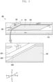
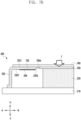
- FIG. 2 is a view illustrating an electronic device 200 according to an embodiment of the present disclosure.
- the electronic device 200 may be at least partially similar to the electronic device 101 in FIG. 1 , or may further include other embodiments of the electronic device.
- the electronic device 200 may include a printed circuit board 210, an electronic component 220, and/or a shield frame 230.
- a length direction of the electronic device 200 may refer to an x-axis direction
- a width direction of the electronic device 200 may refer to a y-axis direction.
- the electronic component 220 and the shield frame 230 may be disposed on one surface of the printed circuit board 210.
- the electronic component 220 may include a processor (e.g., the processor 120 in FIG. 1 ), a communication module (e.g., the communication module 190 in FIG. 1 ), and/or a memory (e.g., the memory 130 in FIG. 1 ).
- a processor e.g., the processor 120 in FIG. 1
- a communication module e.g., the communication module 190 in FIG. 1
- a memory e.g., the memory 130 in FIG. 1 .
- the processor included in the electronic component 220 may be an application processor.
- the shield frame 230 may be disposed on one surface of the printed circuit board 210 while surrounding the electronic component 220.
- the shield frame 230 may serve to shield noise generated from the electronic component 220.
- the noise from the electronic component 220 may cause electromagnetic interference (EMI) that degrades the radio frequency (RF) signal performance of the electronic device 200.
- the shield frame 230 may shield noise generated from the electronic component 220 to reduce electromagnetic interference caused by the noise.
- the shield frame 230 may include a metallic material with a high thermal conductivity to easily conduct heat generated from the electronic component 220 to the outside.
- the shield frame 230 may include at least one of steel, stainless steel, or a copper alloy.
- the shield frame 230 may serve to protect the electronic component 220 from an externally applied impact.
- the shield frame 230 may be a shield can that is formed to have a predetermined thickness.
- the shield frame 230 may be formed to have a thickness of approximately 0.15 mm.
- the shield frame 230 may include a frame opening 231 at least in part.
- the frame opening 231 may be formed at a position corresponding to a position at which the electronic component 220 is disposed.
- at least a portion of the frame opening 231 may be formed at the same position as a position at which the electronic component 220 is disposed with respect to a width direction (e.g., y-axis direction) and a length direction (e.g., x-axis direction) of the electronic device 200.
- the electronic device 200 is illustrated as including one electronic component 220, but the electronic device 200 may include a plurality of electronic components 220.
- the plurality of electronic components 220 may be disposed at a position corresponding to the frame opening 231.
- a length of the frame opening 231 or a length of the electronic component 220 may mean a length that the frame opening 231 or the electronic component 220 extends in a predetermined direction.
- the length of the frame opening 231 may include a length by which the frame opening 231 extends in a length direction of the electronic device 200 (e.g., x-axis direction) or a length by which the frame opening 231 extends in a width direction of the electronic device 200 (e.g., y-axis direction).
- the length of the electronic component 220 may include a length by which the electronic component 220 extends in a length direction of the electronic device 200 (e.g., x-axis direction) or a length by which the electronic component 220 extends in a width direction of the electronic device 200 (e.g., y-axis direction).
- the length of the frame opening 231 may be formed to be longer than the length of the electronic component 220.
- the length by which the frame opening 231 extends in the x-axis direction or the y-axis direction may be formed to be longer than the length by which the electronic component 220 extends in the x-axis direction or the y-axis direction.
- the length of the frame opening 231 is illustrated as being formed longer than the length of the electronic component 220, but this is exemplary and the length of the frame opening 231 may be formed shorter than the length of the electronic component 220.
- the length of the frame opening 231 in the x-axis direction may be formed shorter than the length of the electronic component 220 in the x-axis direction, or the length of the frame opening 231 in the y-axis direction may be formed shorter than the length of the electronic component 220 in the y-axis direction.
- the length of the frame opening 231 when the length of the frame opening 231 is formed to be shorter than the length of the electronic component 220, only a portion of the electronic component 220 may be disposed at a position that overlaps the frame opening 231, and a remaining portion of the electronic component 220 may be disposed at a position that overlaps a position at which the shield frame 230, excluding the frame opening 231, is formed, with respect to a position on the x-y plane.
- the frame opening 231 of the shield frame 230 may serve to prevent the temperature inside the shield frame 230 from rising rapidly due to heat generated by the electronic component 220.
- the shield frame 230 may include an opening side area 232.
- the opening side area 232 is formed on one side of the frame opening 231, and may be an area positioned closer to the electronic component 220 in the width direction (e.g., y-axis direction) or length direction (e.g., x-axis direction) of the electronic device 200 compared to other areas of the shield frame 230.
- the opening side area 232 may be formed in an area of the shield frame 230 positioned in the negative x-axis direction with respect to the frame opening 231.
- the opening side area 232 may be positioned closer to the electronic component 220 in the length direction (e.g., x-axis direction) of the electronic device 200 than other areas of the shield frame 230 positioned in the positive x-axis direction or the positive y-axis direction with respect to the frame opening 231.
- FIG. 3 is a view illustrating the electronic device 200 and the opening side area 232 of the shield frame 230 according to an embodiment of the present disclosure.
- a height direction of the electronic device 200 may mean the z-axis direction.
- the shield frame 230 may include the opening side area 232 at least in part.
- Area A illustrated in FIG. 3 , illustrates an enlarged view of the opening side area 232 of the shield frame 230.
- the opening side area 232 may mean an area of the shield frame 230 that is formed on one side of the frame opening 231.
- the opening side area 232 may be an area positioned in the negative x-axis direction with respect to the frame opening 231.
- the opening side area 232 is illustrated in FIG. 3 as being positioned in the negative x-axis direction with respect to the frame opening 231, the position of the opening side area 232 may not be limited thereto.
- the opening side area 232 may be disposed on a portion of the shield frame 230 positioned in the positive x-axis direction, as well as the negative x-axis direction, or the positive or negative y-axis direction, centered on the frame opening 231.
- the opening side area 232 may include a first surface 2321, a second surface 2322, and/or an inclined surface 2323.
- the first surface 2321 of the opening side area 232 may mean a surface facing vertically in a direction away from the printed circuit board 210.
- the first surface 2321 may be a surface facing vertically in the positive z-axis direction in the opening side area 232.
- the second surface 2322 of the opening side area 232 may mean a surface facing in an opposite direction of the first surface 2321.
- the second surface 2322 may be a surface facing in a direction toward the printed circuit board 210.
- the second surface 2322 may be a surface facing vertically in the negative z-axis direction in the opening side area 232.
- the first surface 2321 of the opening side area 232 may extend longer toward the frame opening 231 in the length direction (e.g., x-axis direction) of the electronic device 200 compared to the second surface 2322 of the opening side area 232.
- the inclined surface 2323 of the opening side area 232 may mean a surface connecting the first surface 2321 and the second surface 2322.
- the inclined surface 2323 of the opening side area 232 may be connected to the first surface 2321 at one end (e.g., an end positioned in the positive z-axis direction with respect to the inclined surface 2323) and connected to the second surface 2322 at the other end (e.g., an end positioned in the negative z-axis direction with respect to the inclined surface 2323).
- the inclined surface 2323 of the opening side area 232 may be a surface that is formed with at least a portion thereof inclined in a direction toward the electronic component 220 with respect to the height direction of the electronic device 200.
- the inclined surface 2323 may be a surface formed with at least a portion thereof inclined in a direction closer to the frame opening 231 with respect to the height direction (e.g., z-axis direction) of the electronic device 200.
- the inclined surface 2323 of the opening side area 232 may be formed with a surface parallel to the height direction (e.g., z-axis direction) of the electronic device 200 and the width direction (e.g., y-axis direction) of the electronic device 200 inclined by a predetermined angle toward the length direction (e.g., x-axis direction) of the electronic device 200.
- the inclined surface 2323 is illustrated as being formed in one direction (e.g., negative x-axis direction) centered on the frame opening 231, but the position at which the inclined surface 2323 is formed may not be limited thereto.
- the inclined surface 2323 may be formed on a portion of the shield frame 230 positioned in the positive x-axis direction, and in the positive or negative y-axis direction, centered on the frame opening 231.
- the inclined surface 2323 may be formed in an area of the shield frame 230 that surrounds the frame opening 231, where a surface area in contact with the shielding sheet 240 (see FIG. 6 ) is formed relatively small.
- one inclined surface 2323 is illustrated as being formed on a portion of the shield frame 230, but a plurality of inclined surfaces 2323 may each be formed on an area of the shield frame 230 that surrounds the frame opening 231.
- the plurality of inclined surface 2323 may each be formed on a portion of the shield frame 230 positioned in the positive x-axis direction, and in the positive or negative y-axis direction, centered on the frame opening 231.
- the inclined surface 2323 of the shield frame 230 may be formed by machining the shield frame 230 in a separate process after the shield frame 230 is manufactured.
- the inclined surface 2323 of the shield frame 230 may be formed in such a way that a chamfer is applied to a portion in which the inclined surface 2323 is required in a mold for manufacturing the shield frame 230.
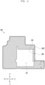
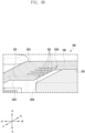
- FIG. 4 is a view illustrating the shield frame 230 according to an embodiment of the present disclosure.
- FIG. 4 is a view illustrating a state of viewing the second surface 2322 of the opening side area 232 of the shield frame 230 according to an embodiment of the present disclosure.
- the shield frame 230 may include a frame opening 231 at least in part.
- the opening side area 232 may be positioned on one side of the frame opening 231.
- An absorbent pad 260 may be disposed on at least a portion of the opening side area 232.
- the absorbent pad 260 may be disposed on the second surface 2322 of the opening side area 232.
- the absorbent pad 260 is illustrated in FIG. 4 as being disposed in the opening side area 232, the position at which the absorbent pad 260 is disposed may not be limited thereto.
- the absorbent pad 260 may be disposed on a portion of the shield frame 230 positioned in the positive x-axis direction, as well as the negative x-axis direction, or the positive or negative y-axis direction, centered on the frame opening 231.
- the absorbent pad 260 may be formed to extend in the length direction (e.g., x-axis direction) and width direction (e.g., y-axis direction) of the electronic device 200.
- the absorbent pad 260 may include a non-conductive material and/or a material capable of absorbing oil.
- the absorbent pad 260 may serve to absorb an oil material 252 (see FIG. 7D ) generated from a heat transfer material 250 (see FIG. 7A ).
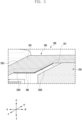
- FIG. 5 is a view illustrating the shield frame 230 in which the absorbent pad 260 is disposed, according to an embodiment of the present disclosure.
- the electronic device 200 may include the absorbent pad 260.
- the absorbent pad 260 may be disposed on at least a portion of the shield frame 230.
- the absorbent pad 260 may be disposed on the second surface 2322 of the opening side area 232 of the shield frame 230.
- the absorbent pad 260 is illustrated in FIG. 5 as being disposed across the entire second surface 2322 of the opening side area 232, the disposition of the absorbent pad 260 is not limited thereto.
- the absorbent pad 260 may be disposed on only a portion of the second surface 2322.
- the absorbent pad 260 may be formed as a plate shape that extends in the length direction (e.g., x-axis direction) and width direction (e.g., y-axis direction) of the electronic device 200 and has a thickness in the height direction (e.g., z-axis direction) of the electronic device 200.
- the opening side area 232 of the shield frame 230 may be positioned spaced apart from the electronic component 220 at a predetermined spacing.
- the first surface 2321, the second surface 2322, and the inclined surface 2323 of the opening side area 232 may be positioned spaced apart from the electronic component 220 in the length direction (e.g., x-axis direction) of the electronic device 200.
- an end of the first surface 2321 positioned closest to the frame opening 231 in the first surface 2321 of the opening side area 232 may be positioned spaced apart from an end of the electronic component 220 (e.g., an end of the electronic component 220 positioned relatively close to the opening side area 232) in the length direction of the electronic device 200.
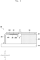
- FIG. 6 is a view illustrating the shield frame 230 in which the shielding sheet 240 is disposed, according to an embodiment of the present disclosure.
- a shielding structure may mean a structure including the shield frame 230, the shielding sheet 240, and/or the absorbent pad 260.
- a length direction and a height direction of the shielding structure may mean the same direction as the length direction and the height direction of the electronic device 200, respectively.
- the length direction of the shielding structure may mean the x-axis direction
- the height direction may mean the z-axis direction.
- a width direction of the shielding structure may mean a direction perpendicular to the x-axis direction and the z-axis direction.
- the shielding sheet 240 may be disposed at least a portion of the shield frame 230.
- the shielding sheet 240 may have at least a portion disposed on the first surface 2321 of the opening side area 232 of the shield frame 230.
- the opening side area 232 may be an area of the shield frame 230 positioned around the circumference of the frame opening 231, where a surface area in contact with the shielding sheet 240 is formed relatively small.
- at least a portion of the shielding sheet 240 may be disposed to cover the frame opening 231 of the shield frame 230.
- the shielding sheet 240 may be disposed in the positive z-axis direction with respect to the frame opening 231 to cover the frame opening 231.
- the shielding sheet 240 may be positioned spaced apart from the electronic component 220 in the height direction (e.g., z-axis direction) of the electronic device 200.
- the shielding sheet 240 may be positioned spaced apart with respect to the electronic component 220 in the positive z-axis direction.
- the shielding sheet 240 may include an adhesive material.
- the shielding sheet 240 may include an adhesive layer that has an adhesive force.
- the shielding sheet 240 may include a tape with an adhesive property. A portion of the shielding sheet 240 including an adhesive material may be adhered to the first surface 2321 of the opening side area 232.
- the shield frame 230 may be disposed spaced apart from the electronic component 220.
- the first surface 2321 of the opening side area 232 of the shield frame 230 may be positioned spaced apart from the electronic component 220 by a first length L1 in the length direction (e.g., x-axis direction) of the electronic device 200.
- the second surface 2322 of the opening side area 232 of the shield frame 230 may be positioned spaced apart from the electronic component 220 by a second length L2 in the length direction (e.g., x-axis direction) of the electronic device 200.
- the inclined surface 2323 of the shield frame 230 may be a surface that is inclined toward the length direction (e.g., x-axis direction) of the electronic device 200 with respect to the height direction (e.g., z-axis direction) of the electronic device 200.
- the second length L2 may be formed longer than the first length L1.
- the first length L1 may be formed to be approximately 0.25 mm
- the second length L2 may be formed to be approximately 0.4 mm.
- the angle at which the inclined surface 2323 of the shield frame 230 is inclined toward the length direction (e.g., x-axis direction) of the electronic device 200 with respect to the height direction (e.g., z-axis direction) of the electronic device 200 may be determined on the basis of a distance between the electronic component 220 and the shield frame 230, a thickness of the shield frame 230, and an amount of heat transfer material 250 (see FIG. 7A ) disposed on the electronic component 220.
- the inclined surface 2323 of the shield frame 230 may be positioned spaced apart from the electronic component 220 in the length direction (e.g., x-axis direction) of the electronic device 200.
- the inclined surface 2323 may be positioned spaced apart from the electronic component 220 by a length that is equal to or greater than the first length L1 and equal to or less than the second length L2 in the length direction (e.g., x-axis direction) of the electronic device 200.
- an angle at which the inclined surface 2323 of the shield frame 230 is inclined with respect to the height direction (e.g., z-axis direction) of the electronic device 200 is illustrated as being constant along the inclined surface 2323 of the shield frame 230, but the angle at which the inclined surface 2323 of the shield frame 230 is inclined may not be limited to one angle.
- the angle at which the inclined surface 2323 of the shield frame 230 is inclined may vary along the inclined surface 2323.
- the absorbent pad 260 may be disposed on the second surface 2322 of the opening side area 232 of the shield frame 230.
- the absorbent pad 260 may be disposed spaced apart from the electronic component 220 by the second length L2 with respect to the length direction (e.g., x-axis direction) of the electronic device 200.
- FIG. 7A , FIG. 7B , FIG. 7C , and FIG. 7D are views illustrating the heat transfer material 250 disposed on the electronic component 220, according to an embodiment of the present disclosure.
- the electronic device 200 may include the heat transfer material 250.
- the heat transfer material 250 may serve to mediate heat generated from the electronic component 220 to be conducted.
- the heat generated by the electronic component 220 may be transferred to the shielding sheet 240 through the heat transfer material 250.
- the shielding sheet 240 may include a heat transfer material.
- the heat transferred to the shielding sheet 240 through the heat transfer material 250 may be transferred to the outside of the shield frame 230 through the heat transfer material included in the shielding sheet 240.
- the heat transfer material 250 may include a solid material and/or a liquid material.
- the heat transfer material 250 may include a gel thermal interface material (GEL TIM).
- the heat transfer material 250 may be disposed on one surface of the electronic component 220.
- at least a portion of the heat transfer material 250 may be disposed on a surface of the electronic component 220 facing in the positive z-axis direction.
- a first direction of the heat transfer material 250 may mean a direction toward the positive z-axis with respect to the heat transfer material 250, and a second direction of the heat transfer material 250 may mean a direction toward the negative z-axis with respect to the heat transfer material 250.
- a spacing space 250a may be formed between the shield frame 230 and the heat transfer material 250.
- the shield frame 230 and the heat transfer material 250 may be disposed spaced apart from each other to form the spacing space 250a.
- the heat transfer material 250 may be disposed between the shielding sheet 240 and the electronic component 220.
- the shielding sheet 240 may be disposed in the first direction of the heat transfer material 250 and the electronic component 220 may be disposed in the second direction of the heat transfer material 250, centered on the heat transfer material 250.
- the shielding sheet 240 may be disposed on the heat transfer material 250 and the shield frame 230.
- the shielding sheet 240 may be disposed in the first direction of the heat transfer material 250 to be in contact with the heat transfer material 250.
- the shielding sheet 240 may be disposed, at least in part, on the first surface 2321 of the opening side area 232 of the shield frame 230. At least a portion of the shielding sheet 240 may be adhered to the first surface 2321 of the opening side area 232.
- the heat transfer material 250 disposed on one surface of the electronic component 220 may be pressed in the height direction (e.g., z-axis direction) of the electronic device 200.
- the shape of the heat transfer material 250 may vary.
- the heat transfer material 250 may include viscous, spreadable, and flowable materials so that the shape of the material may vary while spreading or flowing in response to an externally applied force.
- a force F may be applied from the outside of the shielding sheet 240 in a direction in which the shielding sheet 240 is closer to the electronic component 220 (e.g., negative z-axis direction) in order for at least a portion of the shielding sheet 240 to be adhered to at least a portion of the shield frame 230.
- the force F applied to the shielding sheet 240 may be transmitted to the heat transfer material 250.
- the shape of the heat transfer material 250 may vary as the heat transfer material 250 is subjected to the force.
- the heat transfer material 250 may be subjected to a force that causes at least a portion of the heat transfer material 250 to spread in the length direction and width direction of the electronic device 200.
- a thickness of the heat transfer material 250 may become thinner and a length of the heat transfer material 250 (e.g., a length of the heat transfer material 250 in the x-axis direction) may become relatively longer.
- the shielding sheet 240 is disposed in the first direction of the heat transfer material 250, and a height (e.g., a length in the z-axis direction) of the heat transfer material 250 may be limited. As the shielding sheet 240 is disposed in the first direction of the heat transfer material 250, at least a portion of the heat transfer material 250 may be moved toward the length direction (e.g., x-axis direction) of the electronic device 200.
- the shielding sheet 240 may be disposed on the heat transfer material 250 to press the heat transfer material 250, thereby causing at least a portion of the heat transfer material 250 to move to the spacing space 250a.
- a portion of the heat transfer material 250 disposed in the spacing space 250a may be defined as a diffusion area 251 of the heat transfer material 250.
- the diffusion area 251 of the heat transfer material 250 may be moved toward the spacing space 250a in the length direction (e.g., negative x-axis direction) of the electronic device 200.
- the diffusion area 251 of the heat transfer material 250 may be in contact with a portion of the shield frame 230.
- the diffusion area 251 of the heat transfer material 250 may be in contact with the first surface 2321 of the opening side area 232 of the shield frame 230 that is positioned closest to the heat transfer material 250 of a portion of the shield frame 230.
- the inclined surface 2323 of the shield frame 230 may serve to guide the heat transfer material 250 to flow in a direction toward the printed circuit board 210 (e.g., negative z-axis direction).
- the diffusion area 251 of the heat transfer material 250 may be moved in a direction toward the printed circuit board 210 (e.g., negative z-axis direction).
- the diffusion area 251 of the heat transfer material 250 is prevented by the shield frame 230 and the shielding sheet 240 from being moved in the negative x-axis direction, and may be moved in a direction toward the printed circuit board 210.
- the diffusion area 251 of the heat transfer material 250 may be moved in the negative z-axis direction along a first diffusion path S1.
- the diffusion area 251 of the heat transfer material 250 may be moved along the first diffusion path S1 to come into contact with the printed circuit board 210.
- the oil material 252 included in the heat transfer material 250 may flow out of the heat transfer material 250.
- the oil material 252 may be a material that flows from the heat transfer material 250 due to the high temperature heat generated from the electronic component 220.
- the oil material 252 included in the heat transfer material 250 may flow in a direction toward the shield frame 230 (e.g., negative x-axis direction).
- the inclined surface 2323 of the shield frame 230 may serve to guide a movement path of the oil material 252 so that the oil material 252 generated from the heat transfer material 250 is moved in a direction toward the absorbent pad 260.
- At least a portion of the oil material 252 that flows in a direction toward the shield frame 230 may be absorbed by the absorbent pad 260 disposed on the shield frame 230.
- the oil material 252 discharged from the heat transfer material 250 may move along the second diffusion path S2 and be absorbed into the absorbent pad 260.
- FIG. 8 is a view illustrating the shield frame 230 including a vertical surface 2324, according to an embodiment of the present disclosure.
- the shield frame 230 may include, at least in part, the vertical surface 2324.
- the opening side area 232 of the shield frame 230 may include, at least in part, the vertical surface 2324.
- the vertical surface 2324 may mean a surface that is parallel to the height direction (e.g., z-axis direction) of the electronic device 200 in a portion of the opening side area 232 and perpendicular to the length direction (e.g., x-axis direction) of the electronic device 200.
- the vertical surface 2324 may mean a surface formed perpendicular to a direction in which the heat transfer material 250 (see FIG. 7D ) flows (e.g., x-axis direction).
- the vertical surface 2324 may be connected to the first surface 2321 and the inclined surface 2323 of the opening side area 232.
- the vertical surface 2324 may be connected to the first surface 2321 at one end (e.g., an end of the vertical surface 2324 that is toward the positive z-axis direction) and connected to the inclined surface 2323 at the other end (e.g., an end of the vertical surface 2324 that is toward the negative z-axis direction).
- the inclined surface 2323 may be connected to the vertical surface 2324 at one end and connected to the second surface 2322 of the opening side area 232 at the other end.
- the vertical surface 2324 may extend in the height direction (e.g., z-axis direction) of the electronic device 200 by a third length L3.
- the inclined surface 2323 of the opening side area 232 may extend in the height direction of the electronic device 200 by a fourth length L4.
- the third length L3 may be formed shorter than the fourth length L4, but the relative length relationship between the third length L3 and the fourth length L4 may not be limited thereto.
- the third length L3 may be formed longer than the fourth length L4.
- the vertical surface 2324 of the shield frame 230 may serve to prevent the heat transfer material 250 (see FIG. 7D ) from moving between the shielding sheet 240 (see FIG. 7D ) and the shield frame 230.
- movement of the heat transfer material 250 (see FIG. 7D ) toward the negative x-axis direction may be blocked by the vertical surface 2324 formed perpendicular to the negative x-axis direction, thereby preventing the heat transfer material 250 (see FIG. 7D ) from moving between the shielding sheet 240 (see FIG. 7D ) and the shield frame 230.
- the inclined surface 2323 of the shield frame 230 may not protrude sharply in one direction.
- the shield frame 230 including the vertical surface 2324 may have an effect of preventing the formation of sharp protrusions from the opening side area 232, thereby allowing the manufacturer of the electronic device 200 to safely handle the shield frame 230.
- FIGS. 9A and 9B are views illustrating the shield frame 230 including the exhaust opening 233, according to an embodiment of the present disclosure.
- the shield frame 230 may include the exhaust opening 233 at least in part.
- at least one exhaust opening 233 may be formed in the opening side area 232 of the shield frame 230.
- the exhaust opening 233 may be formed with a portion of the opening side area 232 having a recessed shape.
- the exhaust opening 233 may be formed with a portion of the opening side area 232 recessed in the length direction of the electronic device 200 (e.g., negative x-axis direction).
- the exhaust opening 233 may be formed by passing through the first surface 2321 of the opening side area 232 and the second surface 2322 of the opening side area 232.
- the exhaust opening 233 may be formed in a semicircular shape.
- the exhaust opening 233 may have a semicircular shape formed with a diameter of approximately 0.8 mm or more.
- a plurality of exhaust openings 233 may be formed in the opening side area 232 of the shield frame 230.
- the plurality of exhaust openings 233 may be disposed at predetermined intervals along the width direction (e.g., y-axis direction) of the electronic device 200.
- the plurality of exhaust openings 233 may be disposed spaced apart from each other along the width direction of the electronic device 200 by an interval of approximately 2 mm or more.
- the shield frame 230 is illustrated as including four exhaust openings 233, but the number of exhaust openings 233 that the shield frame 230 includes may not be limited thereto.
- a width of the exhaust opening 233 may mean a length that the exhaust opening 233 extends in the y-axis direction, and a length of the exhaust opening 233 may mean a length that the exhaust opening 233 extends in the x-axis direction.
- each of the plurality of exhaust openings 233 is illustrated as having the same width and length formed, but this is exemplary and the width and length of each of the plurality of exhaust openings 233 may not be limited thereto.
- the width of the exhaust opening 233 and the length of the exhaust opening 233 may be formed differently in each of the exhaust openings 233.
- the exhaust opening 233 may serve to allow the heat transfer material 250 (see FIG. 7D ) to move easily in one direction of the electronic device 200.
- the shielding sheet 240 (see FIG. 7D ) may be disposed in the first direction of the heat transfer material 250 (see FIG. 7D ) and at least a portion of the heat transfer material 250 (see FIG. 7D ) may move toward the exhaust opening 233.
- a portion of the heat transfer material 250 (see FIG. 7D ) that has moved toward the exhaust opening 233 may move from the exhaust opening 233 in the height direction of the electronic device 200 (e.g., negative z-axis direction).
- the heat transfer material 250 (see FIG. 7D ) positioned in the exhaust opening 233 may move in the negative z-axis direction, and the heat transfer material 250 may be prevented from moving between the shielding sheet 240 (see FIG. 7D ) and the shield frame 230.
- the structural rigidity of the shield frame 230 may be maintained, and it may be easier for the heat transfer material 250 (see FIG. 7D ) to move in a direction toward the printed circuit board 210 (see FIG. 7D ) (negative z-axis direction).
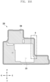
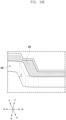
- FIGS. 10A and 10B are views illustrating an insulating pad 234 disposed inside the shield frame 230, according to an embodiment of the present disclosure.
- FIG. 10A is a view illustrating an interior of the shield frame 230, according to an embodiment of the present disclosure.
- FIG. 10B is a view illustrating B area of an area of the shield frame 230 illustrated in FIG. 10A .
- the shield frame 230 may include the insulating pad 234 at least in part of the interior.
- the insulating pad 234 may include an insulating material for preventing shorts inside the shield frame 230 and an adhesive material for adhering the insulating pad 234 to the interior of the shield frame 230.
- the insulating pad 234 may be formed around the frame opening 231 of the shield frame 230 on the interior of the shield frame 230.
- the insulating pad 234 may further include an oil absorbing material capable of absorbing the oil material 252 (see FIG. 7D ), which may serve to absorb the oil material 252 (see FIG. 7D ) generated by the heat transfer material 250 (see FIG. 7D ).
- the oil material 252 may be generated from the heat transfer material 250 (see FIG. 7D ) and flow around the heat transfer material 250 (see FIG. 7D ).
- the oil material 252 (see FIG. 7D ) that flows around the heat transfer material 250 (see FIG. 7D ) may be absorbed by the insulating pad 234 inside the shield frame 230.
- an overall thickness e.g., a length in the z-axis direction
- the pads e.g., the insulating pad 234 and the absorbent pad 260 (see FIG. 5 )
- an overall thickness e.g., a length in the z-axis direction
- the pads e.g., the insulating pad 234 and the absorbent pad 260 (see FIG. 5 )
- an overall thickness may be thinner compared to the shield frame 230 (see FIG. 5 ) having the absorbent pad 260 (see FIG. 5 ) disposed on the outside.
- An electronic device may be one of various types of electronic devices.
- the electronic device may include, for example, a portable communication device (e.g., a smartphone), a computer device, a portable multimedia device, a portable medical device, a camera, a wearable device, or a home appliance.
- a portable communication device e.g., a smartphone
- each of such phrases as “A or B,” “at least one of A and B,” “at least one of A or B,” “A, B, or C,” “at least one of A, B, and C,” and “at least one of A, B, or C,” may include any one of, or all possible combinations of the items enumerated together in a corresponding one of the phrases.
- Such terms as “1st” and “2nd,” or “first” and “second” may be used to simply distinguish a corresponding component from another, and does not limit the components in other aspect (e.g., importance or order).
- constituent element e.g., a first constituent element
- operatively or “communicatively,” as “coupled with,” “coupled to,” “connected with,” or “connected to” another constituent element
- the constituent element may be coupled with the other constituent element directly (e.g., wiredly), wirelessly, or via a third constituent element.
- module used in an embodiment of the present disclosure may include a unit implemented in hardware, software, or firmware, and may interchangeably be used with other terms, for example, "logic,” “logic block,” “component,” or “circuitry”.
- a module may be a single integral component, or a minimum unit or part thereof, adapted to perform one or more functions.
- the module may be implemented in a form of an application-specific integrated circuit (ASIC).
- ASIC application-specific integrated circuit
- An embodiment as set forth herein may be implemented as software (e.g., the program 140) including one or more instructions that are stored in a storage medium (e.g., the internal memory 136 or the external memory 138) that is readable by a machine (e.g., the electronic device 101).
- a processor e.g., the processor 120
- the one or more instructions may include a code generated by a compiler or a code executable by an interpreter.
- the machine-readable storage medium may be provided in the form of a non-transitory storage medium.
- non-transitory simply means that the storage medium is a tangible device, and does not include a signal (e.g., an electromagnetic wave), but this term does not differentiate between where data is semi-permanently stored in the storage medium and where the data is temporarily stored in the storage medium.
- a method according to an embodiment of the present disclosure may be included and provided in a computer program product.
- the computer program product may be traded as a product between a seller and a buyer.
- the computer program product may be distributed in the form of a machine-readable storage medium (e.g., compact disc read only memory (CD-ROM)), or be distributed (e.g., downloaded or uploaded) online via an application store (e.g., PLAYSTORETM), or between two user devices (e.g., smart phones) directly.
- an application store e.g., PLAYSTORETM
- at least part of the computer program product may be temporarily generated or at least temporarily stored in the machine-readable storage medium, such as memory of the manufacturer's server, a server of the application store, or a relay server.
- each constituent element (e.g., module or program), among the above-mentioned constituent elements, may include a single object or a plurality of objects, and some of the plurality of objects may be disposed separately in different constituent elements.
- one or more constituent elements, among the above-mentioned constituent elements, or operations may be omitted, or one or more other constituent elements or operations may be added.
- a plurality of constituent elements (e.g., modules or programs) may be integrated into a single constituent element.
- the integrated constituent element may perform one or more functions of each of the plurality of constituent elements in the same or similar manner as they are performed by a corresponding one of the plurality of constituent elements before the integration.
- operations performed by the module, the program, or another constituent element may be executed sequentially, in parallel, repeatedly, or heuristically, or one or more of the operations may be executed in a different order or omitted, or one or more other operations may be added.
Landscapes
- Engineering & Computer Science (AREA)
- Microelectronics & Electronic Packaging (AREA)
- Chemical & Material Sciences (AREA)
- Physics & Mathematics (AREA)
- Thermal Sciences (AREA)
- Chemical Kinetics & Catalysis (AREA)
- Combustion & Propulsion (AREA)
- Materials Engineering (AREA)
- Organic Chemistry (AREA)
- Shielding Devices Or Components To Electric Or Magnetic Fields (AREA)
Applications Claiming Priority (3)
| Application Number | Priority Date | Filing Date | Title |
|---|---|---|---|
| KR20220079918 | 2022-06-29 | ||
| KR1020220093080A KR20240002645A (ko) | 2022-06-29 | 2022-07-27 | 차폐 구조 및 이를 포함하는 전자 장치 |
| PCT/KR2023/007935 WO2024005401A1 (fr) | 2022-06-29 | 2023-06-09 | Structure de blindage et dispositif électronique la comprenant |
Publications (2)
| Publication Number | Publication Date |
|---|---|
| EP4510801A1 true EP4510801A1 (fr) | 2025-02-19 |
| EP4510801A4 EP4510801A4 (fr) | 2025-08-20 |
Family
ID=89380811
Family Applications (1)
| Application Number | Title | Priority Date | Filing Date |
|---|---|---|---|
| EP23831761.4A Pending EP4510801A4 (fr) | 2022-06-29 | 2023-06-09 | Structure de blindage et dispositif électronique la comprenant |
Country Status (3)
| Country | Link |
|---|---|
| US (1) | US20250081422A1 (fr) |
| EP (1) | EP4510801A4 (fr) |
| WO (1) | WO2024005401A1 (fr) |
Family Cites Families (7)
| Publication number | Priority date | Publication date | Assignee | Title |
|---|---|---|---|---|
| JP6284654B2 (ja) * | 2014-03-18 | 2018-02-28 | 華為終端(東莞)有限公司 | 放熱アセンブリ、及び電子デバイス |
| US10438862B2 (en) * | 2015-12-24 | 2019-10-08 | Mitsubishi Electric Corporation | Electromagnetic shield structure of high frequency circuit and high frequency module |
| KR102583890B1 (ko) * | 2016-02-18 | 2023-10-05 | 삼성전자주식회사 | 열 수집/확산 구조를 가진 전자 장치 |
| US10772245B2 (en) * | 2016-04-04 | 2020-09-08 | Commscope Technologies Llc | Systems and methods for thermal management for high power density EMI shielded electronic devices |
| KR102538757B1 (ko) * | 2018-08-08 | 2023-06-01 | 삼성전자 주식회사 | 쉴드 캔의 개구부를 덮는 도전성 플레이트와 연결된 차폐 부재를 포함하는 전자 장치 |
| DE112021002384T5 (de) * | 2020-06-25 | 2023-02-16 | Hitachi Astemo, Ltd. | Verarbeitungsvorrichtung |
| KR102885259B1 (ko) * | 2020-07-31 | 2025-11-14 | 삼성전자주식회사 | 차폐 및 방열 구조를 포함하는 전자 장치 |
-
2023
- 2023-06-09 EP EP23831761.4A patent/EP4510801A4/fr active Pending
- 2023-06-09 WO PCT/KR2023/007935 patent/WO2024005401A1/fr not_active Ceased
-
2024
- 2024-11-19 US US18/952,435 patent/US20250081422A1/en active Pending
Also Published As
| Publication number | Publication date |
|---|---|
| EP4510801A4 (fr) | 2025-08-20 |
| WO2024005401A1 (fr) | 2024-01-04 |
| US20250081422A1 (en) | 2025-03-06 |
Similar Documents
| Publication | Publication Date | Title |
|---|---|---|
| US11367966B2 (en) | Antenna including conductive pattern and electronic device including antenna | |
| EP3864830B1 (fr) | Module d'antenne et dispositif électronique le comprenant | |
| US11089681B2 (en) | Interposer and electronic device including the same | |
| EP4340125A1 (fr) | Dispositif électronique comprenant une antenne | |
| EP4198685A1 (fr) | Dispositif électronique comprenant un écran souple | |
| US12317407B2 (en) | Electronic device including printed circuit board structure including thermal interface material | |
| US12089384B2 (en) | Electronic device | |
| EP4510801A1 (fr) | Structure de blindage et dispositif électronique la comprenant | |
| KR20240002645A (ko) | 차폐 구조 및 이를 포함하는 전자 장치 | |
| KR20230132331A (ko) | 브릿지 인쇄회로기판을 포함하는 전자 장치 | |
| EP4167689A1 (fr) | Module de carte de circuit imprimé et appareil électronique le comprenant | |
| EP4554338A1 (fr) | Dispositif électronique comprenant un bloc de transfert de chaleur | |
| US12328811B2 (en) | Insulating member arrangement structure and electronic device including the same | |
| EP4676170A1 (fr) | Structure de carte de circuit imprimé recevant un matériau d'interface thermique, et dispositif électronique la comprenant | |
| EP4507469A1 (fr) | Structure de carte de circuit imprimé comprenant un matériau d'interface thermique et dispositif électronique la comprenant | |
| EP4255127A1 (fr) | Dispositif électronique comprenant un interposeur et procédé de fabrication associé | |
| US12520431B2 (en) | Electronic device comprising solder wall | |
| EP4583651A1 (fr) | Dispositif électronique comprenant une partie de transfert de chaleur formant un passage de sortie sonore | |
| US12144115B2 (en) | Electronic device including thermosetting bonding sheet | |
| EP4451814A1 (fr) | Ensemble carte de circuit imprimé comprenant un espaceur ayant une fonction d'auto-alignement, et dispositif électronique le comprenant | |
| US20240292571A1 (en) | Electronic device comprising printed circuit board structure accommodating thermal interface material | |
| EP4565022A1 (fr) | Dispositif électronique comprenant un boîtier de blindage | |
| EP4661222A1 (fr) | Dispositif électronique comprenant un connecteur | |
| US12581598B2 (en) | Electronic device comprising printed circuit board | |
| EP4475635A1 (fr) | Dispositif électronique comprenant une carte de circuit imprimé en pont |
Legal Events
| Date | Code | Title | Description |
|---|---|---|---|
| STAA | Information on the status of an ep patent application or granted ep patent |
Free format text: STATUS: THE INTERNATIONAL PUBLICATION HAS BEEN MADE |
|
| PUAI | Public reference made under article 153(3) epc to a published international application that has entered the european phase |
Free format text: ORIGINAL CODE: 0009012 |
|
| STAA | Information on the status of an ep patent application or granted ep patent |
Free format text: STATUS: REQUEST FOR EXAMINATION WAS MADE |
|
| 17P | Request for examination filed |
Effective date: 20241114 |
|
| AK | Designated contracting states |
Kind code of ref document: A1 Designated state(s): AL AT BE BG CH CY CZ DE DK EE ES FI FR GB GR HR HU IE IS IT LI LT LU LV MC ME MK MT NL NO PL PT RO RS SE SI SK SM TR |
|
| A4 | Supplementary search report drawn up and despatched |
Effective date: 20250717 |
|
| RIC1 | Information provided on ipc code assigned before grant |
Ipc: H05K 9/00 20060101AFI20250711BHEP Ipc: H05K 7/20 20060101ALI20250711BHEP Ipc: C09K 5/14 20060101ALI20250711BHEP Ipc: C09K 5/10 20060101ALI20250711BHEP |
|
| DAV | Request for validation of the european patent (deleted) | ||
| DAX | Request for extension of the european patent (deleted) |