EP4513268A1 - Verfahren zur herstellung von mustern auf einem substrat - Google Patents
Verfahren zur herstellung von mustern auf einem substrat Download PDFInfo
- Publication number
- EP4513268A1 EP4513268A1 EP24194193.9A EP24194193A EP4513268A1 EP 4513268 A1 EP4513268 A1 EP 4513268A1 EP 24194193 A EP24194193 A EP 24194193A EP 4513268 A1 EP4513268 A1 EP 4513268A1
- Authority
- EP
- European Patent Office
- Prior art keywords
- substrate
- etching
- interest
- pads
- thin layer
- Prior art date
- Legal status (The legal status is an assumption and is not a legal conclusion. Google has not performed a legal analysis and makes no representation as to the accuracy of the status listed.)
- Granted
Links
Images


Classifications
-
- G—PHYSICS
- G03—PHOTOGRAPHY; CINEMATOGRAPHY; ANALOGOUS TECHNIQUES USING WAVES OTHER THAN OPTICAL WAVES; ELECTROGRAPHY; HOLOGRAPHY
- G03F—PHOTOMECHANICAL PRODUCTION OF TEXTURED OR PATTERNED SURFACES, e.g. FOR PRINTING, FOR PROCESSING OF SEMICONDUCTOR DEVICES; MATERIALS THEREFOR; ORIGINALS THEREFOR; APPARATUS SPECIALLY ADAPTED THEREFOR
- G03F7/00—Photomechanical, e.g. photolithographic, production of textured or patterned surfaces, e.g. printing surfaces; Materials therefor, e.g. comprising photoresists; Apparatus specially adapted therefor
- G03F7/0002—Lithographic processes using patterning methods other than those involving the exposure to radiation, e.g. by stamping
-
- H—ELECTRICITY
- H10—SEMICONDUCTOR DEVICES; ELECTRIC SOLID-STATE DEVICES NOT OTHERWISE PROVIDED FOR
- H10P—GENERIC PROCESSES OR APPARATUS FOR THE MANUFACTURE OR TREATMENT OF DEVICES COVERED BY CLASS H10
- H10P50/00—Etching of wafers, substrates or parts of devices
- H10P50/60—Wet etching
- H10P50/66—Wet etching of conductive or resistive materials
- H10P50/663—Wet etching of conductive or resistive materials by chemical means only
- H10P50/667—Wet etching of conductive or resistive materials by chemical means only by liquid etching only
-
- H—ELECTRICITY
- H10—SEMICONDUCTOR DEVICES; ELECTRIC SOLID-STATE DEVICES NOT OTHERWISE PROVIDED FOR
- H10P—GENERIC PROCESSES OR APPARATUS FOR THE MANUFACTURE OR TREATMENT OF DEVICES COVERED BY CLASS H10
- H10P50/00—Etching of wafers, substrates or parts of devices
- H10P50/20—Dry etching; Plasma etching; Reactive-ion etching
- H10P50/26—Dry etching; Plasma etching; Reactive-ion etching of conductive or resistive materials
- H10P50/264—Dry etching; Plasma etching; Reactive-ion etching of conductive or resistive materials by chemical means
- H10P50/266—Dry etching; Plasma etching; Reactive-ion etching of conductive or resistive materials by chemical means by vapour etching only
-
- H—ELECTRICITY
- H10—SEMICONDUCTOR DEVICES; ELECTRIC SOLID-STATE DEVICES NOT OTHERWISE PROVIDED FOR
- H10P—GENERIC PROCESSES OR APPARATUS FOR THE MANUFACTURE OR TREATMENT OF DEVICES COVERED BY CLASS H10
- H10P50/00—Etching of wafers, substrates or parts of devices
- H10P50/20—Dry etching; Plasma etching; Reactive-ion etching
- H10P50/28—Dry etching; Plasma etching; Reactive-ion etching of insulating materials
- H10P50/282—Dry etching; Plasma etching; Reactive-ion etching of insulating materials of inorganic materials
- H10P50/283—Dry etching; Plasma etching; Reactive-ion etching of insulating materials of inorganic materials by chemical means
-
- H—ELECTRICITY
- H10—SEMICONDUCTOR DEVICES; ELECTRIC SOLID-STATE DEVICES NOT OTHERWISE PROVIDED FOR
- H10P—GENERIC PROCESSES OR APPARATUS FOR THE MANUFACTURE OR TREATMENT OF DEVICES COVERED BY CLASS H10
- H10P50/00—Etching of wafers, substrates or parts of devices
- H10P50/60—Wet etching
- H10P50/64—Wet etching of semiconductor materials
- H10P50/642—Chemical etching
- H10P50/644—Anisotropic liquid etching
-
- H—ELECTRICITY
- H10—SEMICONDUCTOR DEVICES; ELECTRIC SOLID-STATE DEVICES NOT OTHERWISE PROVIDED FOR
- H10P—GENERIC PROCESSES OR APPARATUS FOR THE MANUFACTURE OR TREATMENT OF DEVICES COVERED BY CLASS H10
- H10P72/00—Handling or holding of wafers, substrates or devices during manufacture or treatment thereof
- H10P72/70—Handling or holding of wafers, substrates or devices during manufacture or treatment thereof for supporting or gripping
- H10P72/74—Handling or holding of wafers, substrates or devices during manufacture or treatment thereof for supporting or gripping using temporarily an auxiliary support
Definitions
- This description relates generally to the field of microelectronics and more particularly to the production of patterns on a substrate with a view to the manufacture of microelectronic components.
- microelectronic components require the creation of patterns on a substrate by photolithography.
- Photolithography is performed through different steps using a resin: spreading the resin on a substrate, exposing the resin using a mask, developing, etching and then removing the resin (or "stripping").
- the removal step (or cleaning the resin) is a complex step because it requires finding a cleaning agent that is aggressive enough to perfectly clean the resin while preserving the integrity of the different surfaces.
- the thin layer comprises a base material, preferably an oxide, and more particularly a silicon oxide, in which pads are arranged, preferably metal pads, and even more preferably copper pads.
- One embodiment provides that the etchant-sensitive material is the base material.
- Another embodiment provides that the etchant-sensitive material corresponds to the pads.
- Another embodiment provides that the method comprises a subsequent step in which the handle substrate is used to pattern another substrate of interest.
- the method comprises a step during which the handle substrate is covered by a protective layer with the etching agent of the sensitive material.
- the protective layer may be an oxide layer or a hydrophobic layer, the hydrophobic layer being able to be formed of one or more compounds chosen from silanes, in particular chlorosilanes, and polymers comprising one or more halogens, preferably fluorinated polymers.
- the expressions “approximately”, “approximately”, “substantially”, and “of the order of” mean to within 10%, preferably to within 5%.
- the handle substrate 100 forms a hard mask. It makes it possible to form patterns 250 on the substrate of interest without implementing photolithography steps. The method is thus simple and quick to implement.
- handle substrate 100 it is possible to form patterns on multiple substrates (wafers).
- the handle substrate is reusable, which further reduces process costs.
- step a it is possible to carry out one or more pre-treatments on the surface of the handle substrate 100 and/or on the surface of the substrate of interest 200 so as to make them compatible with direct bonding.
- Pretreatment can be chosen from the following pre-treatments: thermal annealing, plasma, polishing and wet cleaning.
- an oxide layer on the surface of the handle substrate 100 and/or to perform a polishing step on the handle substrate 100 and/or on the substrate of interest 200 to obtain a roughness compatible with direct bonding (typically a roughness of less than 0.5 nm RMS).
- a roughness compatible with direct bonding typically a roughness of less than 0.5 nm RMS.
- step a the handle substrate 100 and the substrate of interest 200 are brought into contact to be bonded.
- the two substrates 100, 200 can be assembled by direct bonding.
- the use of marks on the substrates 100, 200 can facilitate their alignment.
- a precision of approximately 100nm can be achieved. It is also possible to align them, without using marks, by using the edges of the substrates as well as their notch. The precision is lower (+/- 50 ⁇ m) but sufficient for certain applications.
- Direct bonding can be carried out at atmospheric pressure (i.e. 1013.25 hPa) or under vacuum.
- the assembly does not necessarily need to be consolidated by heat treatment.
- annealing preferably at a temperature below 200°C, can be advantageously carried out.
- the handle substrate 100 comprises a base 110 and raised elements 120 (pillars or columns).
- the surface of the elements 120 can be of different shapes. It can be square, rectangular or even circular.
- the raised elements 120 have, for example, a height of between 1 ⁇ m and 200 ⁇ m or more specifically between 10 ⁇ m and 100 ⁇ m. These elements 120 are preferably spaced apart by more than 10 ⁇ m or even more than 50 ⁇ m in order to allow the infiltration of the etching agent (gaseous or liquid) by capillarity within the network formed by the raised elements 120.
- the base 110 and the relief elements may be made of different materials. Preferably, they are made of the same material.
- the handle substrate 100 is preferably obtained from a solid substrate. It may be a substrate made of metal or semiconductor material for example.
- Trimming the plate edge makes it possible to avoid possible edge contact between the handle substrate 100 and the substrate of interest 200.
- the trimming can be done for example by photolithography/etching, or by mechanical trimming using a diamond saw.
- the width of the trimming is, for example, between 1 and 5 mm and/or its depth is, for example, between 100 and 250 ⁇ m.
- the patterns 250 formed on the substrate of interest 200 by the vertical etching can also undergo horizontal etching, which thus modifies their lateral dimensions.
- This lateral etching effect can be taken into account in the dimensioning of the elements 120 in relief in order to be able to obtain patterns 250 having the desired dimensions.
- the etching agent etches not only the material sensitive to the etching agent, but also the sides of the raised elements 120 of the handle substrate 100.
- the lateral dimension of the elements 120 of the handle substrate 100 is also reduced by a few tens of micrometers. If this handle substrate 100 is used again, the patterns 250 etched on the new substrate of interest will therefore have a smaller dimension than that obtained during the previous use.
- a tolerance on the dimensional variations of a few tens of micrometers is acceptable.
- This protective layer can be made of a material hydrophobic which will prevent the action of aqueous etching solutions or in a material inert with respect to the etching agent (or at least having a low etching speed by the etching agent). It is also possible to choose a handle substrate made of a material inert with respect to the etching agent (or at least having a low etching speed by the etching agent).
- the protective layer is an oxide layer 135.
- the oxide layer is inert with respect to the etching agent.
- the oxide layer 135 can have a thickness of between 20 nm and 5000 nm.
- the layer can also be called a film. It can be a thermal oxide, a native oxide or a deposited oxide, for example by chemical deposition of silicon alkoxide such as tetraethyl orthosilicate (TEOS) or silane in the vapor phase assisted or not by a plasma.
- TEOS tetraethyl orthosilicate
- the oxide layer 135 can completely cover the relief elements 120 of the substrate 100 ( figure 3 ). It does not interfere with gluing.
- the oxide film is present over the entire handle substrate 110.
- a handle substrate 100 covered with a layer of silicon oxide will be used to form patterns 250 on a substrate of interest 200 made of silicon or a metal such as copper. Since silicon oxide is not very sensitive to silicon etching agents (such as KOH, TMAH or a HF/HNO 3 mixture) or to etching agents for metals such as copper (for example solutions formed from a mixture of H 2 SO 4 /H 2 O 2 /H 2 O), the handle substrate 100 will not be etched and the geometry and dimensions of the raised elements 120 will be preserved.
- silicon etching agents such as KOH, TMAH or a HF/HNO 3 mixture
- metals such as copper
- the handle substrate 100 may be partially or completely covered by a hydrophobic layer 130.
- the hydrophobic layer 130 acts as a barrier to the aqueous etching agent.
- the hydrophobic layer 130 may be inorganic or organic.
- the layer may also be called a film.
- hydrophobic layer 130 will depend on the handle substrate 100, the substrate of interest 200 and the etching solution 300.
- the hydrophobic layer 130 has, for example, a thickness of between 2 and 1000 nm.
- hydrophobic layer 130 obtained from a polymer or a silyl (also called organosilyl).
- the selected hydrophobic compound preferably comprises one or more halogen groups, in particular fluorine or chlorine groups.
- the hydrophobic compound comprises a carbon chain of at least 5 carbon atoms.
- OTS octadecyltrichlorosilane
- the polymers may be fluorinated polymers such as, for example, the Novec TM 1720 EGC polymer marketed by the company 3M TM , Optool marketed by the company DAIKIN and the Novec TM 2202 EGC polymer marketed by the company 3M TM .
- FDTS perfluorodecyltrichlorosilane
- FDDMCS perfluorodecyldimethylchlorosilane
- the hydrophobic layer 130 is deposited by liquid means.
- the side walls (flanks) of the raised elements 120 of the handle substrate 100 are covered with a hydrophobic film 130.
- the thickness of the hydrophobic film 130 is, for example, of the order of ten nanometers.
- the parts of the handle substrate 100 not exposed to the hydrophobic compound are compatible with a direct bonding process.
- the temporary substrate 400 may be recycled, for example, by implementing an oxygen plasma treatment followed by wet cleaning.
- the hydrophobic film 130 will make contact between the surface of the handle substrate 100 and the etching solution 300 impossible. Only the material sensitive to the etching agent of the substrate of interest 100 to be structured is etched, while preserving the morphology of the raised elements 120 of the handle substrate 100.
- a handle substrate 100 and a substrate of interest 200 will be used, the etching speeds of which are considerably different in the presence of an etching agent.
- the etching solution 300 does not etch the handle substrate or only slightly.
- the handle substrate 100 and the thin layer 220 to be structured are made of different materials.
- the material forming the handle substrate 100 may have a crystalline orientation different from that of the thin layer 120 to be structured of the substrate of interest 100.
- the crystalline orientation will be chosen so that the etching rate of the handle substrate 100 in the etching solution is lower than the etching rate of the layer 220 in the etching solution 300.
- the ⁇ 111> planes of silicon have a much lower etching rate by TMAH, TEAH or KOH than the exposed ⁇ 001> surface. This therefore makes it possible to greatly limit lateral etching by revealing ⁇ 111> planes.
- the substrate of interest 200 comprises the support substrate 210 covered by the thin layer 220 comprising at least one material sensitive to an etching agent.
- the substrate of interest 200 may be an SOI ('Silicon on Insulator') substrate, i.e. comprising a support substrate 210 covered by a thin layer of buried oxide and a layer of silicon 220.
- the thin layer of oxide may act as an etching stop layer (vertical etching).
- it may be a solid substrate 210 made of semiconductor material (silicon for example) covered with a dielectric layer 220, in particular an oxide layer (silicon oxide in particular).
- elements 240 may be arranged. These elements 240 form vertical walls in the thin layer 220. These elements 240 surround the second zones Z2. These are protective barriers 240 making it possible to stop lateral over-etching, which can sometimes accompany the vertical etching of the etched material. The width of this barrier will be chosen so as to be sufficiently large to stop over-etching.
- the elements 240 may have identical or different shapes. They are, of course, made of a material different from the material sensitive to the etching agent.
- the positioning of the elements 240 is preferably chosen so that, when bonding the handle substrate 100 and the substrate of interest 200, the elements 240 are positioned totally or partially under the raised elements of the handle substrate 100.
- the second zones Z2 to be protected are thus not exposed to the etching agent.
- a lateral tolerance is also conceivable.
- one of the relief elements 120 may protrude from the desired location of the pattern 250 or be offset from the desired location of the pattern 250.
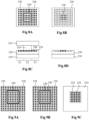
- the relief element 120 may, for example, have a larger surface area than the surface to be protected positioned between the protective barriers 240 ( Figure 5A ) or a misalignment may exist between the relief elements 120 and the protective barriers 240, the protective barriers 240 thus protruding from the relief element 120 ( Figures 5B and 5C ).
- the etching is effective and stops on the protective barrier 240. It is obvious that this case has limits and that the under-etching width is chosen so as not to be too large, for example a few tens of microns is acceptable. Preferably, 1 mm will not be exceeded and, more specifically, 500 pm will not be exceeded.
- the thin layer 220 may comprise a base material (oxide in particular) and pads 230, in particular metal pads ( Figures 7A to 7D , 8A to 8D and 9A to 9C ).
- the base material is not etched, and a thin layer 220 is obtained comprising a plurality of holes (blind or passing through the thin layer 220) and patterns 250 in relief ( Figures 7A to 7D ).
- the holes are obtained by removing the pads 230.
- the relief patterns 250 correspond to the second parts Z2 of the thin layer 220 which was protected by the relief elements 120 of the handle substrate 100.
- the thin layer 120 comprises a base material, protective barriers 240 and pads 230.
- the 230 pads may be surrounded by a protective layer to protect them during the etching step.
- a protective layer to protect them during the etching step.
- layers of Ti and TiN or Ta and TaN may surround copper 230 pads. Specific etching types may then be used for these materials.
- the protective barriers of the base material 240 and the pads 230 are sensitive to the same etching agent.
- the protective barriers 240 are preferably made of the same material as the pads 230. Even more preferably, it is a metal, such as copper.
- the base material is an oxide, for example a silicon oxide.
- the protective barriers 240 and the pads 230 can thus be removed during a single etching step ( Figures 8A to 8D ). We thus obtain a thin layer 220 comprising a plurality of holes (blind or passing through the thin layer). 220) at the level of the first zones Z1.
- the second zones Z2 of the thin layer 220 opposite the relief elements 120 are preserved during the etching step.
- the base material is sensitive to the etching agent.
- the protective barriers 240 and the pads 230 are not sensitive to the etching agent ( Figure 9A ).
- the protective barriers 240 and the pads 230 may be made of the same material or of different materials.
- the protective barriers 240 and the pads 230 are made of metal, preferably copper.
- the base material is, for example, an oxide, and in particular a silicon oxide.
- the protective barriers 240 and the metal pads 230 not sensitive to the etching element are preserved during the etching step ( Figure 9B ).
- a structure is obtained comprising relief patterns 250 surrounded by protective barriers 240.
- the relief patterns 250 comprise the base material in which the pads 230 are dispersed.
- the patterns 250 may be surrounded by the protective barriers 240. Between the patterns 250, the support substrate 210 is covered by the metal pads 230 ( Figure 9B ).
- the metal barriers 240 and/or the metal pads 230 can be inserted into the oxide layer, for example with a Damascene type process.
- metallic barriers 240 and/or metallic pads 230 made of copper inserted in a layer of silicon oxide.
- the metal barriers 240 and/or the metal pads 230 may be formed, for example, by physical vapor deposition (PVD) and/or by electrochemical deposition (ECD).
- PVD physical vapor deposition
- ECD electrochemical deposition
- layers of Ti, TiN and Cu will be deposited beforehand by PVD.
- Deposition by ECD makes it possible to form elements of greater thickness than PVD. It is also possible to replace the Ti and TiN layers with layers of Ta and TaN. The Ti/TiN or Ta/TaN layers act as a barrier to the diffusion of copper into the silicon.
- the assembly can be rinsed by immersion and dried. Drying can be carried out by centrifugation.
- the obtained substrate of interest 200 comprises a support substrate covered by the relief patterns 250.
- the thickness of the patterns depends on the intended application.
- the patterns can be formed from a base material ( Figure 6D ) or a base material in which 230 studs are dispersed ( Figure 7D ).
- An element 240 can surround the patterns ( Figure 9B ).
- the handle substrate 100 can be used in a new gluing/etching cycle. Cleaning is advantageously carried out between each use.
- the substrates are made from 200 mm diameter silicon wafers.
- a silicon wafer (handle substrate 100) undergoes oxidation so as to obtain a 100 nm film of silicon oxide on the surface.
- a photolithography/etching process makes it possible to form silicon oxide pads of 10 x 10 mm 2 and a thickness of 100 ⁇ m (100 nm of SiO 2 and 99.9 ⁇ m of silicon).
- the edge of the wafer 100 is trimmed with a diamond saw with a width of 3 mm and a depth of 200 ⁇ m.
- the oxide surface of the wafer 100 is cleaned by an O 2 plasma followed by CARO, SC1 wet cleaning. so as to make it compatible with a direct bonding process.
- An SOI wafer (substrate of interest 200) having a support substrate 220 covered by a 205 nm silicon film 220 and a 400 nm buried oxide layer undergoes CARO/SC1 wet cleaning to make it compatible with a direct bonding process.
- the two substrates 100, 200 are directly bonded to each other.
- the assembly is immersed for 10 s in a 1% HF solution 300, then rinsed in deionized water. A second etching of 3 min is then carried out at 70°C in an aqueous solution of TMAH at 5% by mass. The assembly is then rinsed by immersion in water and then dried by centrifugation.
- the handle substrate 100 is removed by inserting a wedge into the structure.
- a plate of interest 200 comprising a silicon support substrate on which are arranged silicon pads 250 of 10 x 10 mm 2 with a thickness of 205 nm.
- a silicon wafer (handle substrate 100) is produced as described in example 1. It has relief elements 120 (rectangular pads) of 10 x 5mm 2 and a thickness of 15 ⁇ m.
- a silicon wafer (temporary substrate 400) is prepared so as to make it compatible with direct bonding.
- the temporary substrate 400 and the handle substrate 100 are directly bonded.
- the assembly is immersed in a 310 solution of OTS (octadecyltrichlorosilane) in isooctane and then rinsed in isooctane.
- OTS octadecyltrichlorosilane
- the silicon wafer 100 has bonding sites in the form of rectangular pads 120 15 ⁇ m high, the environment including the sides of which is covered with a hydrophobic film 130.
- An SOI wafer (substrate of interest 200) comprising a support substrate 210 covered by a 205 nm silicon film 220 and a 400 nm buried oxide layer undergoes CARO/SC1 wet cleaning to make it compatible with a direct bonding process.
- the substrate of interest 200 and the handle substrate 100 are directly bonded.
- the assembly is immersed for 10 s in a 300 solution of HF at 1%, then rinsed in DI water.
- a second etching of 3 min is then carried out at 70 ° C in an aqueous solution of TMAH at 5% by mass intended to etch the silicon.
- the buried oxide layer of the substrate of interest allows the etching to be stopped.
- the assembly is then rinsed by immersion in water and then dried by centrifugation.
- the handle substrate 100 is disassembled by inserting a wedge into the structure.
- the hydrophobic film 130 has made it possible to protect the silicon forming the raised elements 120 of the substrate 100, the dimensions of which have not been altered, from etching.
- a plate of interest 200 comprising a silicon support substrate on which are arranged rectangular silicon patterns 250 of 10 x 5 mm 2 with a thickness of 205 nm.
- Photolithography/etching is performed on a silicon wafer (handle substrate 100) to form cylindrical elements 120 with a diameter of 10 mm and a thickness of 60 ⁇ m.
- the edge of the handle substrate 100 is trimmed with a diamond saw: 5 mm wide and 200 ⁇ m deep.
- This wafer is oxidized to form a 400 nm oxide film on the surface.
- An SOI wafer (substrate of interest 200) comprises a support substrate 210 covered by a 205 nm silicon film 220 and a 400 nm buried oxide layer.
- the substrate of interest 200 undergoes CARO/SC1 wet cleaning to make it compatible with a direct bonding process.
- This substrate is immersed for 10 s in an etching solution 300 (1% HF), then rinsed in DI water.
- the two substrates 100, 200 are directly bonded.
- the assembly is immersed for 3 min at 70°C in an aqueous solution of TMAH at 5% by mass intended to etch the silicon.
- TMAH aqueous solution intended to etch the silicon.
- the buried oxide layer of the substrate of interest 200 allows the etching to be stopped.
- the assembly is then rinsed by immersion in water and then dried by centrifugation.
- the plate (handle substrate 100) is dismantled by inserting a wedge into the structure.
- the 400 nm oxide film present on the surface of this substrate 100 has made it possible to protect the raised elements 120 of the substrate from silicon etching, the dimensions of which have not been altered.
- a substrate 200 comprising a silicon support substrate on which are arranged cylindrical silicon patterns 250 with a diameter of 10 mm and a thickness of 205 nm.
- a photolithography/etching process makes it possible to form relief elements 120 of 10 x 10 mm 2 and a thickness of 100 ⁇ m.
- the edge of this substrate 100 is trimmed with a diamond saw: with a width of 3 mm and a depth of 200 ⁇ m.
- the surface of the wafer 100 is cleaned by an O 2 plasma followed by CARO, SC1 wet cleaning so as to make it compatible with a direct bonding process.
- a wafer (substrate of interest 200) undergoes oxidation so as to form a 100 nm oxide film 220 on its surface.
- This wafer 200 is wet cleaned so as to make it compatible with a direct bonding process.
- the two substrates 100, 200 are directly bonded.
- the assembly is annealed at 150°C for 2 hours and then immersed for 3 minutes in an aqueous solution of HF at 5% by volume intended to etch the silicon oxide.
- the stack can be treated by exposing it to HF vapors.
- the assembly is then rinsed by immersion in water and then dried by centrifugation.
- the handle substrate 100 is dismantled by inserting a wedge into the structure.
- a 200 silicon plate of interest is obtained which has 250 cylindrical silicon oxide patterns of 10 x 5 mm 2 and a thickness of 100 nm.
- a silicon wafer (substrate-handle 100) is produced as described in example 1. It has rectangular pads of 10 x 5mm 2 with a thickness of 15 ⁇ m.
- a wafer substrate of interest 200
- 400 nm of oxide is deposited from TEOS.
- layers of Ti, TiN and Cu with a thickness of 10, 50 and 200 nm are deposited by PVD.
- an electrochemical treatment by ECD allows a 1000 nm Cu film to be deposited.
- a copper polishing step removes a 200 nm thickness of copper and allows the surface of the substrate 200 to be prepared for direct bonding.
- the two substrates 100, 200 are directly bonded.
- the assembly is immersed for 2 min in a 300 aqueous solution of DSP (H 2 SO 4 /H 2 O 2 /H 2 O in a proportion of 1/2/50) in order to etch the copper layers.
- DSP H 2 SO 4 /H 2 O 2 /H 2 O in a proportion of 1/2/50
- This assembly is immersed in a SC1 solution at 70°C for 2 min in order to etch the Ti and TiN layers. The assembly is then rinsed by immersion in water and then dried by centrifugation.
- the plate (handle substrate 100) is dismantled by inserting a wedge into the structure.
- a silicon plate (substrate of interest 200) is obtained which has 250 rectangular copper patterns of 10 x 5 mm 2 with a thickness of 1000 nm.
- a silicon wafer (handle substrate 100) is produced as described in example 1. It has rectangular elements 120 of 5 x 5mm 2 with a thickness of 15 ⁇ m.
- a checkerboard of 230 copper pads surrounded by a thin protective layer of Ti/TiN within an oxide layer is produced as shown in Figure 9A .
- a 240 protective barrier copper surrounds the Z2 areas.
- the repeat pitch of the 230 copper pads is 5pm for 230 square copper pads of 2.5pm on each side.
- the copper barrier is 2.5pm wide instead of two rows and columns of copper pads.
- the Ti and TiN layers are 10nm and 50nm thick.
- the thickness of the 230 copper pads is 500nm. They are manufactured using a classic copper damascene process with Ti/TiN protective layers. A chemical-mechanical polishing is carried out after the damascene process in order to make the surface compatible with a hybrid direct bonding process.
- the two substrates 100, 200 are aligned and glued.
- the assembly After bonding, the assembly is annealed at 150°C for 2 hours. The assembly is then immersed for 3 minutes in a 5% volume aqueous HF solution intended to etch the silicon oxide. The assembly is then rinsed by immersion in water and then dried by centrifugation. The configuration obtained is that of Figure 9B .
- the two substrates 100, 200 can be peeled off and thus areas of interest are obtained that are compatible with future direct bonding on another plate of interest. It is also possible not to peel off the two substrates 100, 200 and to etch the copper pads 230 not protected by the raised elements 120 and/or the protective barrier 240.
- the assembly is immersed for 2 min in an aqueous solution of DSP (H 2 SO 4 /H 2 O 2 /H 2 O in a proportion of 1/2/50) so as to etch the copper.
- the assembly is then rinsed by immersion in water and then dried by centrifugation.
- This assembly is then immersed in a SC1 solution at 70°C for 2 min so as to etch the Ti and TiN layers.
- the assembly is then rinsed by immersion in water and then dried by centrifugation.
- the resulting assembly corresponds to the configuration of the Figure 9C .
- the two substrates 100, 200 can then be peeled off.
Landscapes
- Physics & Mathematics (AREA)
- General Physics & Mathematics (AREA)
- Weting (AREA)
- ing And Chemical Polishing (AREA)
- Laminated Bodies (AREA)
Applications Claiming Priority (1)
| Application Number | Priority Date | Filing Date | Title |
|---|---|---|---|
| FR2308799A FR3152190B1 (fr) | 2023-08-18 | 2023-08-18 | Procédé de réalisation de motifs sur un substrat |
Publications (2)
| Publication Number | Publication Date |
|---|---|
| EP4513268A1 true EP4513268A1 (de) | 2025-02-26 |
| EP4513268B1 EP4513268B1 (de) | 2026-04-01 |
Family
ID=88965341
Family Applications (1)
| Application Number | Title | Priority Date | Filing Date |
|---|---|---|---|
| EP24194193.9A Active EP4513268B1 (de) | 2023-08-18 | 2024-08-12 | Verfahren zur herstellung von mustern auf einem substrat |
Country Status (3)
| Country | Link |
|---|---|
| US (1) | US12288694B2 (de) |
| EP (1) | EP4513268B1 (de) |
| FR (1) | FR3152190B1 (de) |
Citations (2)
| Publication number | Priority date | Publication date | Assignee | Title |
|---|---|---|---|---|
| US20110017705A1 (en) * | 2008-01-03 | 2011-01-27 | Laurent Jalabert | Method for Local Etching of the Surface of a Substrate |
| US20170372917A1 (en) * | 2016-06-28 | 2017-12-28 | Taiwan Semiconductor Manufacturing Co., Ltd. | Pattern transfer technique and method of manufacturing the same |
Family Cites Families (6)
| Publication number | Priority date | Publication date | Assignee | Title |
|---|---|---|---|---|
| US4734152A (en) * | 1986-12-22 | 1988-03-29 | Massachusetts Institute Of Technology | Dry etching patterning of electrical and optical materials |
| EP0710432B1 (de) * | 1994-05-18 | 2004-01-02 | Dyconex AG | Verfahren zur herstellung von folienleiterplatten oder halbzeugen für folienleiterplatten sowie nach dem verfahren hergestellte folienleiterplatten und halbzeuge |
| US7202179B2 (en) * | 2004-12-22 | 2007-04-10 | Hewlett-Packard Development Company, L.P. | Method of forming at least one thin film device |
| JP2008053250A (ja) * | 2006-08-22 | 2008-03-06 | Sony Corp | 半導体装置の製造方法 |
| JP2009231595A (ja) * | 2008-03-24 | 2009-10-08 | Oki Data Corp | 半導体素子製造方法 |
| US8480942B2 (en) * | 2010-01-27 | 2013-07-09 | The Board Of Trustees Of The University Of Illinois | Method of forming a patterned layer of a material on a substrate |
-
2023
- 2023-08-18 FR FR2308799A patent/FR3152190B1/fr active Active
-
2024
- 2024-08-12 EP EP24194193.9A patent/EP4513268B1/de active Active
- 2024-08-14 US US18/804,455 patent/US12288694B2/en active Active
Patent Citations (2)
| Publication number | Priority date | Publication date | Assignee | Title |
|---|---|---|---|---|
| US20110017705A1 (en) * | 2008-01-03 | 2011-01-27 | Laurent Jalabert | Method for Local Etching of the Surface of a Substrate |
| US20170372917A1 (en) * | 2016-06-28 | 2017-12-28 | Taiwan Semiconductor Manufacturing Co., Ltd. | Pattern transfer technique and method of manufacturing the same |
Non-Patent Citations (1)
| Title |
|---|
| PARK SEONG-JUN ET AL: "Fabrication of graphite grids via stencil lithography for highly sensitive motion sensors", CARBON, ELSEVIER OXFORD, GB, vol. 96, 25 September 2015 (2015-09-25), pages 491 - 496, XP029314392, ISSN: 0008-6223, DOI: 10.1016/J.CARBON.2015.09.080 * |
Also Published As
| Publication number | Publication date |
|---|---|
| US20250062134A1 (en) | 2025-02-20 |
| EP4513268B1 (de) | 2026-04-01 |
| US12288694B2 (en) | 2025-04-29 |
| FR3152190A1 (fr) | 2025-02-21 |
| FR3152190B1 (fr) | 2025-07-18 |
Similar Documents
| Publication | Publication Date | Title |
|---|---|---|
| EP3593376B1 (de) | Verfahren zur selbstassemblierung von mikroelektronischen bauteilen | |
| EP1210733A1 (de) | Herstellung von durchkontakten durch ein substrat | |
| EP1759411B1 (de) | Verfahren zur übertragung von platten | |
| EP2676288B1 (de) | Verfahren zur herstellung einer substrathalterung | |
| EP4513268B1 (de) | Verfahren zur herstellung von mustern auf einem substrat | |
| EP0273792A1 (de) | Verfahren zur Herstellung von Elementen mit Zwischenraum | |
| FR3108439A1 (fr) | Procede de fabrication d’une structure empilee | |
| EP4513269B1 (de) | Verfahren zur strukturierung eines substrats | |
| WO2006075081A1 (fr) | Composant micromecanique avec des elements actifs et procede de realisation d'un tel composant | |
| EP4202981A1 (de) | Verfahren zum direkten verbinden von elektronischen bauteilen | |
| EP4152373A2 (de) | Verfahren zur herstellung eines elektronischen schaltkreises für die selbstmontage an einem anderen elektronischen schaltkreis | |
| FR2983343A1 (fr) | Procede de prevention d'une panne electrique dans un empilement de couches semi-conductrices, cellule cpv a substrat mince, et assemblage de cellule solaire | |
| EP4300553A1 (de) | Selbstausgerichtete bindung durch hydrophiliekontrast | |
| EP4579728A1 (de) | Verfahren zur herstellung hydrophober bereiche auf einem substrat | |
| FR3009128A1 (fr) | Procede de realisation d'un plot conducteur sur un element conducteur | |
| EP4280261A1 (de) | Verfahren zum temporären verkleben | |
| EP3171395A1 (de) | Herstellung von verbindungen durch umbiegen von leiterelementen unter eine mikroelektronische vorrichtung wie einen chip | |
| EP4704162A1 (de) | Speichervorrichtung und herstellungsverfahren | |
| EP0338636A1 (de) | Verfahren zum Herstellen von elektrischen Kontakten von kleiner Dimension auf einer Halbleiterschaltung | |
| WO2024133079A1 (fr) | Procédé de fabrication d'une plaque comprenant deux zones ayant un contraste de mouillabilité supérieur à 90° et plaque ainsi fabriquée | |
| EP3772746A1 (de) | Verfahrenzur herstellung von durchgangsverbindungen durch ein substrat | |
| WO2019186035A1 (fr) | Procédé de fabrication d'un substrat donneur pour la réalisation d'une structure intégrée en trois dimensions et procédé de fabrication d'une telle structure intégrée | |
| FR3050865A1 (fr) | Procede de realisation d'interconnexions conductrices sur un substrat et interconnexions ainsi obtenues | |
| EP0994506A1 (de) | Verfahren zur Herstellung des Kondensators einer Speicherzelle |
Legal Events
| Date | Code | Title | Description |
|---|---|---|---|
| PUAI | Public reference made under article 153(3) epc to a published international application that has entered the european phase |
Free format text: ORIGINAL CODE: 0009012 |
|
| STAA | Information on the status of an ep patent application or granted ep patent |
Free format text: STATUS: REQUEST FOR EXAMINATION WAS MADE |
|
| 17P | Request for examination filed |
Effective date: 20240812 |
|
| AK | Designated contracting states |
Kind code of ref document: A1 Designated state(s): AL AT BE BG CH CY CZ DE DK EE ES FI FR GB GR HR HU IE IS IT LI LT LU LV MC ME MK MT NL NO PL PT RO RS SE SI SK SM TR |
|
| GRAP | Despatch of communication of intention to grant a patent |
Free format text: ORIGINAL CODE: EPIDOSNIGR1 |
|
| STAA | Information on the status of an ep patent application or granted ep patent |
Free format text: STATUS: GRANT OF PATENT IS INTENDED |
|
| INTG | Intention to grant announced |
Effective date: 20251212 |
|
| GRAS | Grant fee paid |
Free format text: ORIGINAL CODE: EPIDOSNIGR3 |
|
| GRAA | (expected) grant |
Free format text: ORIGINAL CODE: 0009210 |
|
| STAA | Information on the status of an ep patent application or granted ep patent |
Free format text: STATUS: THE PATENT HAS BEEN GRANTED |
|
| AK | Designated contracting states |
Kind code of ref document: B1 Designated state(s): AL AT BE BG CH CY CZ DE DK EE ES FI FR GB GR HR HU IE IS IT LI LT LU LV MC ME MK MT NL NO PL PT RO RS SE SI SK SM TR |
|
| REG | Reference to a national code |
Ref country code: CH Ref legal event code: F10 Free format text: ST27 STATUS EVENT CODE: U-0-0-F10-F00 (AS PROVIDED BY THE NATIONAL OFFICE) Effective date: 20260401 Ref country code: GB Ref legal event code: FG4D Free format text: NOT ENGLISH |
|
| REG | Reference to a national code |
Ref country code: IE Ref legal event code: FG4D Free format text: LANGUAGE OF EP DOCUMENT: FRENCH |
|
| REG | Reference to a national code |
Ref country code: DE Ref legal event code: R096 Ref document number: 602024003604 Country of ref document: DE |