EP4513527A2 - Gasvermittelte sekundärelektronenerzeugung und sammlungsverstärkung für verbesserte endpunktdetektion mit edelionen zur schaltungsbearbeitung in halbleiterwafern - Google Patents
Gasvermittelte sekundärelektronenerzeugung und sammlungsverstärkung für verbesserte endpunktdetektion mit edelionen zur schaltungsbearbeitung in halbleiterwafern Download PDFInfo
- Publication number
- EP4513527A2 EP4513527A2 EP24182807.8A EP24182807A EP4513527A2 EP 4513527 A2 EP4513527 A2 EP 4513527A2 EP 24182807 A EP24182807 A EP 24182807A EP 4513527 A2 EP4513527 A2 EP 4513527A2
- Authority
- EP
- European Patent Office
- Prior art keywords
- gas
- inspection
- ion beam
- gases
- repair
- Prior art date
- Legal status (The legal status is an assumption and is not a legal conclusion. Google has not performed a legal analysis and makes no representation as to the accuracy of the status listed.)
- Pending
Links
Images





Classifications
-
- G—PHYSICS
- G03—PHOTOGRAPHY; CINEMATOGRAPHY; ANALOGOUS TECHNIQUES USING WAVES OTHER THAN OPTICAL WAVES; ELECTROGRAPHY; HOLOGRAPHY
- G03F—PHOTOMECHANICAL PRODUCTION OF TEXTURED OR PATTERNED SURFACES, e.g. FOR PRINTING, FOR PROCESSING OF SEMICONDUCTOR DEVICES; MATERIALS THEREFOR; ORIGINALS THEREFOR; APPARATUS SPECIALLY ADAPTED THEREFOR
- G03F1/00—Originals for photomechanical production of textured or patterned surfaces, e.g., masks, photo-masks, reticles; Mask blanks or pellicles therefor; Containers specially adapted therefor; Preparation thereof
- G03F1/68—Preparation processes not covered by groups G03F1/20 - G03F1/50
- G03F1/72—Repair or correction of mask defects
- G03F1/74—Repair or correction of mask defects by charged particle beam [CPB], e.g. focused ion beam
-
- H—ELECTRICITY
- H01—ELECTRIC ELEMENTS
- H01J—ELECTRIC DISCHARGE TUBES OR DISCHARGE LAMPS
- H01J37/00—Discharge tubes with provision for introducing objects or material to be exposed to the discharge, e.g. for the purpose of examination or processing thereof
- H01J37/26—Electron or ion microscopes; Electron or ion diffraction tubes
- H01J37/28—Electron or ion microscopes; Electron or ion diffraction tubes with scanning beams
-
- H—ELECTRICITY
- H10—SEMICONDUCTOR DEVICES; ELECTRIC SOLID-STATE DEVICES NOT OTHERWISE PROVIDED FOR
- H10P—GENERIC PROCESSES OR APPARATUS FOR THE MANUFACTURE OR TREATMENT OF DEVICES COVERED BY CLASS H10
- H10P74/00—Testing or measuring during manufacture or treatment of wafers, substrates or devices
- H10P74/20—Testing or measuring during manufacture or treatment of wafers, substrates or devices characterised by the properties tested or measured, e.g. structural or electrical properties
- H10P74/203—Structural properties, e.g. testing or measuring thicknesses, line widths, warpage, bond strengths or physical defects
-
- G—PHYSICS
- G03—PHOTOGRAPHY; CINEMATOGRAPHY; ANALOGOUS TECHNIQUES USING WAVES OTHER THAN OPTICAL WAVES; ELECTROGRAPHY; HOLOGRAPHY
- G03F—PHOTOMECHANICAL PRODUCTION OF TEXTURED OR PATTERNED SURFACES, e.g. FOR PRINTING, FOR PROCESSING OF SEMICONDUCTOR DEVICES; MATERIALS THEREFOR; ORIGINALS THEREFOR; APPARATUS SPECIALLY ADAPTED THEREFOR
- G03F1/00—Originals for photomechanical production of textured or patterned surfaces, e.g., masks, photo-masks, reticles; Mask blanks or pellicles therefor; Containers specially adapted therefor; Preparation thereof
- G03F1/68—Preparation processes not covered by groups G03F1/20 - G03F1/50
- G03F1/82—Auxiliary processes, e.g. cleaning or inspecting
- G03F1/84—Inspecting
- G03F1/86—Inspecting by charged particle beam [CPB]
-
- H—ELECTRICITY
- H01—ELECTRIC ELEMENTS
- H01J—ELECTRIC DISCHARGE TUBES OR DISCHARGE LAMPS
- H01J37/00—Discharge tubes with provision for introducing objects or material to be exposed to the discharge, e.g. for the purpose of examination or processing thereof
- H01J37/02—Details
- H01J37/04—Arrangements of electrodes and associated parts for generating or controlling the discharge, e.g. electron-optical arrangement or ion-optical arrangement
- H01J37/08—Ion sources; Ion guns
-
- H—ELECTRICITY
- H01—ELECTRIC ELEMENTS
- H01J—ELECTRIC DISCHARGE TUBES OR DISCHARGE LAMPS
- H01J37/00—Discharge tubes with provision for introducing objects or material to be exposed to the discharge, e.g. for the purpose of examination or processing thereof
- H01J37/26—Electron or ion microscopes; Electron or ion diffraction tubes
-
- H—ELECTRICITY
- H01—ELECTRIC ELEMENTS
- H01J—ELECTRIC DISCHARGE TUBES OR DISCHARGE LAMPS
- H01J37/00—Discharge tubes with provision for introducing objects or material to be exposed to the discharge, e.g. for the purpose of examination or processing thereof
- H01J37/30—Electron-beam or ion-beam tubes for localised treatment of objects
-
- H—ELECTRICITY
- H01—ELECTRIC ELEMENTS
- H01J—ELECTRIC DISCHARGE TUBES OR DISCHARGE LAMPS
- H01J37/00—Discharge tubes with provision for introducing objects or material to be exposed to the discharge, e.g. for the purpose of examination or processing thereof
- H01J37/30—Electron-beam or ion-beam tubes for localised treatment of objects
- H01J37/305—Electron-beam or ion-beam tubes for localised treatment of objects for casting, melting, evaporating, or etching
- H01J37/3053—Electron-beam or ion-beam tubes for localised treatment of objects for casting, melting, evaporating, or etching for evaporating or etching
-
- H—ELECTRICITY
- H01—ELECTRIC ELEMENTS
- H01J—ELECTRIC DISCHARGE TUBES OR DISCHARGE LAMPS
- H01J37/00—Discharge tubes with provision for introducing objects or material to be exposed to the discharge, e.g. for the purpose of examination or processing thereof
- H01J37/30—Electron-beam or ion-beam tubes for localised treatment of objects
- H01J37/305—Electron-beam or ion-beam tubes for localised treatment of objects for casting, melting, evaporating, or etching
- H01J37/3053—Electron-beam or ion-beam tubes for localised treatment of objects for casting, melting, evaporating, or etching for evaporating or etching
- H01J37/3056—Electron-beam or ion-beam tubes for localised treatment of objects for casting, melting, evaporating, or etching for evaporating or etching for microworking, e. g. etching of gratings or trimming of electrical components
-
- H—ELECTRICITY
- H01—ELECTRIC ELEMENTS
- H01J—ELECTRIC DISCHARGE TUBES OR DISCHARGE LAMPS
- H01J37/00—Discharge tubes with provision for introducing objects or material to be exposed to the discharge, e.g. for the purpose of examination or processing thereof
- H01J37/32—Gas-filled discharge tubes
- H01J37/32431—Constructional details of the reactor
- H01J37/3244—Gas supply means
-
- H—ELECTRICITY
- H10—SEMICONDUCTOR DEVICES; ELECTRIC SOLID-STATE DEVICES NOT OTHERWISE PROVIDED FOR
- H10P—GENERIC PROCESSES OR APPARATUS FOR THE MANUFACTURE OR TREATMENT OF DEVICES COVERED BY CLASS H10
- H10P34/00—Irradiation with electromagnetic or particle radiation of wafers, substrates or parts of devices
- H10P34/40—Irradiation with electromagnetic or particle radiation of wafers, substrates or parts of devices with high-energy radiation
-
- H—ELECTRICITY
- H10—SEMICONDUCTOR DEVICES; ELECTRIC SOLID-STATE DEVICES NOT OTHERWISE PROVIDED FOR
- H10W—GENERIC PACKAGES, INTERCONNECTIONS, CONNECTORS OR OTHER CONSTRUCTIONAL DETAILS OF DEVICES COVERED BY CLASS H10
- H10W20/00—Interconnections in chips, wafers or substrates
- H10W20/01—Manufacture or treatment
- H10W20/031—Manufacture or treatment of conductive parts of the interconnections
- H10W20/067—Manufacture or treatment of conductive parts of the interconnections by modifying the pattern of conductive parts
-
- H—ELECTRICITY
- H01—ELECTRIC ELEMENTS
- H01J—ELECTRIC DISCHARGE TUBES OR DISCHARGE LAMPS
- H01J2237/00—Discharge tubes exposing object to beam, e.g. for analysis treatment, etching, imaging
- H01J2237/004—Charge control of objects or beams
- H01J2237/0041—Neutralising arrangements
-
- H—ELECTRICITY
- H01—ELECTRIC ELEMENTS
- H01J—ELECTRIC DISCHARGE TUBES OR DISCHARGE LAMPS
- H01J2237/00—Discharge tubes exposing object to beam, e.g. for analysis treatment, etching, imaging
- H01J2237/006—Details of gas supplies, e.g. in an ion source, to a beam line, to a specimen or to a workpiece
-
- H—ELECTRICITY
- H01—ELECTRIC ELEMENTS
- H01J—ELECTRIC DISCHARGE TUBES OR DISCHARGE LAMPS
- H01J2237/00—Discharge tubes exposing object to beam, e.g. for analysis treatment, etching, imaging
- H01J2237/30—Electron or ion beam tubes for processing objects
- H01J2237/317—Processing objects on a microscale
- H01J2237/3174—Etching microareas
- H01J2237/31742—Etching microareas for repairing masks
- H01J2237/31744—Etching microareas for repairing masks introducing gas in vicinity of workpiece
-
- H—ELECTRICITY
- H01—ELECTRIC ELEMENTS
- H01J—ELECTRIC DISCHARGE TUBES OR DISCHARGE LAMPS
- H01J2237/00—Discharge tubes exposing object to beam, e.g. for analysis treatment, etching, imaging
- H01J2237/30—Electron or ion beam tubes for processing objects
- H01J2237/317—Processing objects on a microscale
- H01J2237/31749—Focused ion beam
Definitions
- the invention provides an ion beam inspection and repair system and method with increased secondary electron emission. With the system and method, inspection and editing of deep structures is improved. The method is applicable for circuit edit within semiconductor wafers or EUV mask repair.
- circuit edit refers to a modification of integrated circuits in semiconductor wafers of dies.
- Circuit editing involves physically modifying integrated circuits to remove, add or otherwise modify materials to alter a semiconductor feature in a semiconductor chip or wafer, enable additional circuit functionality, characterize the operation of the circuit, or correct the function or reliable performance of an integrated circuit.
- circuit edits are performed during the initial stages of the integrated circuit's life cycle to understand or improve the product's performance. Circuit edits are often performed because they can quickly enable the inexpensive prototyping of a circuit modification before the substantial investment in new lithographic masks and repeating the many steps involved in the wafer fabrication process.
- the methods make use of a radiation beam, for example a Laser beam or a charged particle beam.
- the radiation beam is focused onto a region of repair, where a layer of material is either removed or deposited.
- precursor gases are provided at a repair site to either provide the material for deposition or to bond to the removed material.
- etching gases are used to augment the removal process to make it more effective, more uniform, or more or less selective in the milling of one sample material relative to another.
- electron or focused ion beams are utilized for editing or repair operations.
- Focused Ion Beam (FIB) systems for example, provide lateral resolutions down to the nanometer regime, and a precise editing or repair of mask or semiconductor features is possible.
- the pattern of material removal such as trenches or holes of almost arbitrary shape can be formed with high precision.
- the milling rate or rate at which the milled depth increases versus time depends on the various factors, including the material composition of the sample, the geometry of the milled region, the ion current of the focused ion beam as well as the kinetic energy of the ions, and the mass of the ions.
- the achieved milling depth may further be subject to several uncertainties, like energy spread of the ions, fluctuations in the ion beam current, fluctuations in material compositions, crystallographic orientation, or sample charging, and the like.
- Some focused Ion Beam systems of the prior art use Gallium as the ion species.
- a FIB beam current can vary over many orders of magnitude, with a conventional gallium FIB this can span from a few pA to several nA.
- the areal dosages used by a gallium FIB can be on the order of 1E14 ions/cm ⁇ 2 or more, for example 1E15, 1E16 or higher ions /cm ⁇ 2.
- a gas field ion beam system has been described.
- US 8,110,114 B2 describes the use of an ion beam system using a gas field ion source and an activating gas for deposition or removal of material for circuit editing. According to US 8,110,114 B2 , using a gas field ion source, an unwanted gallium implantation into a semiconductor substrate is avoided.
- a gas field ion beam system of the prior art for mask repair is described in US 9,236,225 B2 .
- the computer designed patterns of a lithography mask typically have feature sizes comparable to the feature sizes or CD to be produced in the microelectronic circuits on a wafer. Therefore, for microelectronic circuits on a wafer as well as the features on lithography masks, dimensions of features or patterns are becoming ever smaller, for example below 20nm, below 10nm, below 5nm, below 3nm or even less. With these actual and future critical dimensions (CD), also the placement of the semiconductor features or mask features becomes more and more demanding.
- the pattern placement is typically correlated with the overlay requirement, which is typically specified by a fraction of the CD, for example 1/3 or less of the CD. According to the overlay requirement, the features in different layers within a micro-electronic circuit on a wafer must overlap with even higher precision, with deviations for example below 2nm or even below 1nm.
- Semiconductor masks typically have a topography formed by the absorbing structures on top of the mask material.
- Absorbing structures are typically formed by lithographic processing of an opaque film, for example a chrome film of up to a thickness of tens of nm.
- Other materials or structures can be employed as well, for example for phase shift masks.
- For EUV masks also other absorbers can be employed as for example thin tantalum films or silicon nitride.
- Features for phase shifting in EUV masks can be buried features, which are covered by a reflective multi-layer stack.
- NAND memory devices of processors comprise about 100 layers, and even higher numbers of layers will be achieved in near future.
- Each layer may be formed as a conducting layer, with conducting features embedded within isolating material.
- the layers may be separated by isolating layers with some vias or through connections.
- Isolating material is typically formed by Silicon oxide or Silicon Nitride, while conducting features are formed by doped silicon or metals, comprising for example copper, aluminum, or tungsten.
- each layer is planarized and a next layer is formed on top of it.
- the layer thickness can thus be very small, for example 50nm, 20nm, 10nm or even less.
- a repair site or circuit edit site might be covered by a multi-layer structure comprising up to 100 or even more thin semiconductor layers.
- the same layered structure applies to EUV masks.
- EUV masks typically are formed by at least one multilayer-stack comprising at least thirty or more mono-layers of Molybdenum and Silicon. In this case, each layer pair has a thickness of about a half of the EUV wavelength of 13.4nm. Further thin diffusion barrier layers may be formed between the layers.
- An improved method of ion beam milling and ion beam inspection and an improved ion beam system for inspection and for repair utilizes means for an increase of a secondary electron yield.
- the improved ion beam system is capable for an ion beam inspection or milling with increased secondary electron yield.
- a secondary electron signal is increased during ion beam milling or ion beam inspection, and for example an accuracy of an end-pointing is improved.
- an accuracy of an editing method for a deep structure within or below a multi-layer stack is improved.
- a precision-controlled removal of a multi-layer stack above a deep structure is enabled by an ion beam milling with increased secondary electron yield.
- a circuit editing or mask repair with a lateral accuracy of below 1nm and a milling accuracy in depth of below 1nm is enabled.
- a method of ion beam scanning a semiconductor sample is comprising providing at least two individual gases of a group of gases selected for an increase of a secondary electron yield (short: SE-enhancement gases) by at least two individual gas nozzles to the inspection or repair site.
- the group of SE-enhancement gases is comprises gases including:
- the method is further comprising arranging an inspection or repair site of a wafer at a column axis of an ion beam column and starting a scanning operation of the ion beam over the inspection or repair site.
- a first gas for SE-enhancement is selected from a group of gases including Hydrogen, Oxygen, water vapor, H2O2, XeF2, NF3, nitric acid, N,N-dimethyl ethanamide, formic acid, ethanol, isopropanol, methyl nitro acetate, ammonia, ammonium Carbamate and nitro-ethanol.
- a second gas for SE-enhancement is selected from a group of gases including Nitrogen, Neon, Xenon, Argon, Krypton and Helium.
- a third gas for SE-enhancement is selected from a group of gases including XeF2, CI2, Bromine vapor, Iodine vapor, and water vapor.
- the at least two gases for SE-enhancement are selected based on a predetermined material composition at an inspection or repair site of a wafer.
- the material composition of a layer at the inspection or repair site can be determined from CAD information of the mask or wafer or can be determined from a scanning ion beam image obtained during ion beam scanning.
- the material composition of each of the many layers within a mask or wafer can be different, and the selection and partial pressure of the at least two gases can be adjusted and changed according to the material composition of an actual layer of a mask or wafer. Thereby, for example an end point of a milling operation and stopping the scanning operation of the ion beam over the inspection or repair site can be determined with improved precision.
- an inspection and repair system is comprising an ion beam column and a group of individual gas nozzles with individual control valves.
- the group of individual gas nozzles is comprising at least a first and a second individual gas nozzle.
- the inspection and repair system is further comprising a control module configured to control during use a gas supply of at least a first and a second individual gas for secondary electron enhancement via the at least first and second individual gas nozzles.
- the control module further comprises a memory storing a set of instructions, and a processor configured to execute the set of instructions to cause the inspection and repair system to perform a method of ion beam scanning with increased secondary electron yield.
- the control module is configured for selecting and providing during use at least two individual gases of a group of gases selected for an increase of a secondary electron yield (short: SE-enhancement gases) by at least two individual gas nozzles.
- the at least first and second individual gas nozzles are connected to at least two gas reservoirs comprising at least two gases selected from a first, a second and a third gas of a group of SE-enhancement gases.
- the first gas for SE-enhancement can be selected from a group of gases including Hydrogen, Oxygen, water vapor, H2O2, XeF2, NF3, nitric acid, N,N-dimethyl ethanamide, formic acid, ethanol, isopropanol, methyl nitro acetate, ammonia, ammonium Carbamate and nitro-ethanol.
- the second gas for SE-enhancement can selected from a group of gases including Nitrogen, Neon, Xenon, Argon, Krypton and Helium.
- the third gas for SE-enhancement can be selected from a group of gases including XeF2, Cl2, Bromine vapor, Iodine vapor, and water vapor.
- the inspection and repair system is further comprising a stage control and a stage for arranging an inspection or repair site of a wafer or mask at a column axis of an ion beam column.
- the inspection and repair system is comprising a further gas nozzle to provide a gas selected from a group of gases including PMPCS, Tungsten Hexacarbonyl, dicobalt octa carbonyl, molybdenum hexacarbonyl, and silazane.
- a dedicated coating can be locally generated, for example a Tungsten coating, and an alignment fiducial can be generated, or a repair operation can be performed.
- the ion beam column of the inspection and repair system comprises a gas field ion source.
- Typical ions used in gas field ion sources are Helium, Neon, Xenon, Argon, but other gases and other kinds of ion sources for focused ion beams are possible as well.
- This disclosure describes certain advantageous techniques for achieving successful circuit edits or mask repairs at the smallest scales.
- the described techniques involve a focused ion beam system (FIB), and a novel method of using a focused ion beam.
- Factors such as redeposition and enhanced sputter yield at different angles are factors that experts in this field will be familiar with. Experts in this field are also familiar with enhancement of the milling rate with the addition of etching gases facilitating higher material removal rates or making them more or less selective to different materials or different crystalline orientations.
- a FIB column can for example be a Gallium FIB, with or without a Wien filter or similar mechanism to allow alloy-based sources (such as silicon, gold, etc.), or a FIB with a gas field ion source (GFIS), plasma source or duo-plasmatron with other kinds of ion species, such as Xenon, Oxygen or Argon ions or related technologies (for example "cluster” or "low temperature” ion sources).
- GFIS gas field ion source
- plasma source or duo-plasmatron with other kinds of ion species, such as Xenon, Oxygen or Argon ions or related technologies (for example "cluster” or "low temperature” ion sources).
- a FIB column is used to produce focused ion beams, optionally at different charge states of ions or different ions.
- an inspection and repair system 1 capable of increased secondary electron yield.
- An example of the inspection and repair system 1 is illustrated in Figure 1 .
- the system 1 comprises a source chamber 351 with a gas field ion source 349 for generating an ion beam 103, an ion beam column 353, and a sample enclosure 355.
- the inspection and repair system 1 is operated at high vacuum and connected to several vacuum pumps (not shown).
- the source tip 301 is provided and connected via a heating wire 303 to mounting posts 305.
- the source tip 301 can be formed by few atoms, for example one or three atoms of tungsten.
- the source chamber 351 is further connected to a vacuum pump (not shown), by which a low vacuum pressure inside the source chamber 351 is maintained.
- An ion species is generated at the source tip 301.
- the ion species depends on the gas provided by gas nozzles 341.1 and 341.2 into the evacuated source chamber 351.
- the source gas nozzles 341 are connected to gas supply units (not shown) for connecting the source chamber to different source gases.
- the source gas nozzles 341 are configured with precision valves 347.1 and 347.2, by which the partial gas pressures inside the source chamber 351 is adjusted.
- two source gas supply nozzles 341.1, 341.2 are shown, for providing two different noble gases, for example Helium 343 and Neon 345.
- gas nozzles 341 can be provided and further gases can be used as well, including other noble gases like Argon, or other gases from materials of low atomic mass, for example Lithium or Nitrogen.
- the ions generated at source tip 301 are accelerated by the extractor electrode to a kinetic energy of up to 30keV.
- an ion beam energy can be adjusted to lower energies as well, for example below 20keV, 10 keV, for example 6 keV, 5 keV, 4 keV, or 1 keV.
- the gas atoms 343, now ionized and passing the aperture of the extractor electrode 307, are leaving the source chamber 351 through an aperture and are collimated and focused by at least one condenser lens 309 to form an intermediate source image 314.
- the condenser lens 309 can comprise several lenses, by which for example a magnification of the source image 314 can be adjusted. Thereby, a source current and a resolution can be adjusted.
- the condenser lens 309 can be configured as an electrostatic lens comprising at least three electrode plates. However, the condenser lens 309 can also be a magnetic lens or a combination of magnetic and electrostatic lenses.
- the sample 7 is mounted in a sample chamber 355 on a sample stage 500, which can be moved and controlled in six degrees of freedom.
- sample stages 500 are known in the art and comprise for example laser interferometers or similar means for position control.
- sample stages 500 further comprise means for precision actuation, such as piezoelectric actuators.
- a stage 500 can comprise a first stage with long stroke actuators and a second stage with short stroke actuators with precision control within the nm-region.
- a repair or inspection site 41 is arranged in proximity of the column axis 359, with the sample surface 15 perpendicular to the column axis 359.
- the sample stage 500 is configured to hold the sample surface in the focus plane of the ion beam column 353.
- a decelerating voltage VE can be provided to the sample 7. With the sample voltage VE, a further adjustment of the focus position is possible. Further, a sample current corresponding to the absorbed charge from the ion beam 103 can be measured. A further calibration sample 339 can be provided on the sample stage 500.
- the sample enclosure 355 is further connected to a vacuum pump system, comprising such as a turbo-molecular pump, an ion pump, a getter pump, a cryo-pump, a titanium sublimation pump or the like (not shown).
- the process chamber 355 is provided with a load lock (not shown) for transfer of the sample 7.
- a detector 331 is arranged in proximity of the interaction volume of the ion beam 103 with the sample 7.
- the detector 331 is configured to attract secondary electrons, which are generated by interaction of the ion beam 103 with the sample 7 and are attracted along path 333.
- the detector 331 comprises a charged grid to attract electrons, a scintillator to convert charged particles to photons, a light guide, and a photon-detector such as a PMT.
- the inspection and repair system 1 further comprises at least one gas nozzle 335 of a first group of gas nozzles, connected to a reservoir of a precursor gas 337, selected for example for a beam-induced deposition of a material.
- the precursor gas 337 is for example selected from a group of gases including PMPCS, Tungsten Hexacarbonyl, dicobalt octa carbonyl, molybdenum hexacarbonyl, and silazane.
- a source control module 801 is responsible for controlling during use a source operation.
- the source control module 801 is connected to the voltage supply for providing the source voltage VS and extractor voltage (not shown).
- the source control module 801 is connected to the precision valves 347.1 and 347.2, by which the source gas concentration can be adjusted during use.
- the source control module 801 is further connected to the condenser lens 309 and the first and second multi-pole elements 311 and 313, by which the formation of the intermediate source image 314 is controlled.
- Source control unit 801 is further connected to the aperture stop carrier 315, which is configured for a change of the apertures stop 317.1 or 317.2 during use.
- Source control module 801 is further connected to beam dump 321 and configured for determining and controlling the ion beam current during use.
- a focusing control unit 807 is connected to the objective lens 329 and the sample voltage supply. Focusing control unit 807 is configured to adjust the focus spot position of focus spot 105 on the surface of the sample 7.
- An image acquisition control unit 803 is connected to image sensor 331 and scanning deflectors 323, 325 and 327. During an image acquisition or milling operation, the focused ion beam 103 is scanning deflected in a predetermined scanning path across the surface of the sample 7, and the intensity signal of interaction products 333 is detected for each scanning position and stored in memory locations corresponding to the scanning position in a memory of the image acquisition unit 803. Thereby, image acquisition and scanning are performed during use in synchronized operation and a 2D image of an area of the sample surface is obtained.
- a first scanning operation of the ion beam 103 is controlled by the third and fourth multi-pole elements 323 and 325. With the combined action of the third and fourth multi-pole elements 323 and 325, a deflection position of the ion beam 103 and an angle of incidence of the ion beam 103 at the surface of the sample 7 can be adjusted.
- a typical scanning frequency of about 0.01 Hz to 100 Hz can be achieved, corresponding to a pixel dwell time between 0.5 ⁇ s to 100 ⁇ s.
- a fine adjustment of a position of the focus points of the ion beam 103 can be achieved by the fifth deflector 327.
- the multipole elements 323, 325 and 327 can further act either alone or in combination to adjust or compensate an aberration of the ion beam 103. Thereby, a small probe size with high resolution of below 3nm or even less can be achieved with a position accuracy of below 1nm.
- the objective lens 329 can be formed by a stack of multipole elements, and the focusing control unit 807 is configured to drive each multi-pole element with an offset voltage to generate a lens function and with a plurality of additional individual voltages which are configured to scanning deflect the ion beam 103 and to compensate aberrations of the ion beam 103.
- the source control module 801 is configured for a precise control of an ion beam current down to currents below few pA, for example below 1pA, or even below 0.1pA. With the source control module 801, it is further possible to select and adjust ion species during use.
- the repair system 1 is using a gas field ion source (GFIS) with Neon 343 and Helium 345 for circuit edit or repair operation.
- GFIS gas field ion source
- the inspection and repair system 1 is configured for using Neon ions for milling and Helium ions for imaging.
- the source control module 801 is configured for supplying Neon 343 by opening precision valve 347.1 into the source chamber 351 and for providing a source voltage VS to the source tip 1.
- the inspection and repair system 1 can further be configured to operate at one or more ion species in the ion beam 103.
- the inspection and repair system 1 further comprises at least one individual gas nozzle 635.1 to 635.3 of a second group of gas nozzles.
- the individual gas nozzle 635.1 to 635.3 of a second group of gas nozzles are arranged for the individual supply of different gases 637 of a group of SE-enhancement gases separately to the processing chamber 355.
- the system 1 comprises three gas nozzles 635.1, 635.2 and 635.3.
- Each individual gas nozzle 635.i is provided with a valve (only one valve 661.1 shown) and connected to at least one reservoir of a specified gas.
- Each individual gas nozzle 635.i is connected to a voltage supply for providing a bias voltage VB to an individual gas nozzle 635.i.
- Operation control unit 800 is further connected to inspection control module 811, which is configured to control a gas supply of specified gases 637 via gas nozzles 635.1, 635.2 and 635.3 with control valves 661.1 to 661.3 (only one valve shown in figure 1 ).
- Inspection control module 811 is configured to select and provide individual gases 637 to the processing chamber 355 in dependence of an inspection or repair task.
- a typical inspection or repair task is illustrated at the example of a circuit edit operation at a semiconductor wafer in Figure 2 .
- a simplified model of a semiconductor wafer 7 with several layers 75.1 to 75.N of different composition is shown in cross section in Figure 2a .
- the figure illustrates an example of a circuit edit operation at a repair site 41 and shows the result of the preliminary steps to prepare the semiconductor wafer 7 at the repair site 41.
- a circuit edit or repair location 81 is in repair layer 75.E, which is covered by many layers.
- a layer number of a deep repair layer 75.E may be at least E > 10, E > 30, E > 50, E > 80 or even E > 100.
- Each layer of the multilayer structure is comprising for example conductors such as aluminum, tungsten or copper embedded in semiconductor materials such as doped silicon, silicon oxide or silicon nitride.
- Figure 2b shows a top view of the same repair location 41.
- a local trench 43 is created into the surface 15 at the area surrounding the edit site 41 to allow for better access.
- the location of the inspection site 41 and of the trench 43 can be based on different information, for example a failure analysis of the semiconductor wafer 7 or CAD information and can be aided by optical or infrared microscopy which can penetrate the remaining silicon and see navigation fiducials 51.1 and 51.2 before performing the milling operation of trench 43.
- Navigation fiducials 51 are typically present in the fabricated semiconductor wafer 7.
- the trench 43 can be created by micro-scale techniques which include laser processing, masked etching using a plasma FIB with etch masks, or FIB operating with high beam currents.
- the lateral extension of the trench 43 can be several 10 ⁇ m, for example 50 ⁇ m 100 ⁇ m, 200 ⁇ m or even more.
- the depth of the trench is selected down to surface 17, which is selected slightly above and nearly exposing the surface 19 of the first semiconductor layer 75.1 of active devices, which are the object of the circuit edit task.
- the exposed or nearly exposed navigation fiducials 51.1 to 51.4 serve as alignment markers which can be used as location references relative to CAD information (i.e., blueprints) for the subsurface design features of interest.
- CAD information i.e., blueprints
- the semiconductor wafer 7 can be registered with respect to for example CAD information and subsequent activities can be aligned with high precision in lateral X, Y -direction to access the subsurface features at repair location 81 that require editing.
- a local trench 45 is formed by precision FIB milling to fully expose a present alignment fiducial 51.1.
- a further alignment fiducial 33 is formed close to a lateral position of the repair location 81.
- a second trench 47 can be formed to expose the surface 19 of the first layer 75.1. Deep milling through the stack of multi-layers 75.1 to 75.E is performed to form deep trench 49 down to the repair location 81.
- a precision Ion beam milling with low beam energies and low beam currents is applied. By utilizing low beam energies and low beam currents, the precision milling proceeds slowly, and sub-surface defects are minimized. During the precision milling down to the repair location 81, features present in the layers 75.1 to 75.E are necessarily destroyed.
- the extent of the deep trench 49 is kept small.
- the depth of the formation of trench 49 by precision milling down to the repair location 81 is determined by an end-pointing method incorporating a monitoring of the increased rate of secondary electrons collected during ion beam milling.
- the number of electrons which escape from the surface of the substrate that is related to the electron emission or electron yield of the material itself, and on the charge state of the sample surface.
- the charge state of the sample 7 tends to build up positively which has the tendency to suppress secondary electron escape.
- Insulators such as dielectric materials such as SiO2 have the tendency to build up significant positive charge very quickly. Therefore, parts of the secondary electrons generated are not collected by an external electron detector because the positive surface charges prevent secondary electrons from leaving the sample.
- one way of mitigating this accumulated positive charge is by using an electron "flood gun," which is used in parallel with the primary ion beam to introduce a neutralizing negative charge to the sample surface. Electrons provided in excess, however, also might have a negative effect by generating a negative surface charge and by deteriorating the ion beam.
- the inspection and repair system 1 is configured to provide a gas flow of individual different gases prior, concurrently, or alternatingly with an ion-beam exposure or irradiation of the sample surface 15 at an inspection or repair site 41.
- the focused ion beam system 1 comprises a focused ion beam column configured for an irradiation of a surface 15 of a sample 7 by a primary charged ion beam (e.g., a focused Neon Ion beam) and at least one individual gas nozzle 635.1 to 635.3 selected from a second group of gas nozzles including
- the first gas 637.1 is selected from a group of gases including oxidizing or reducing agents such as Hydrogen, Oxygen, water vapor, H2O2, XeF2, NF3, nitric acid, N,N-dimethyl ethanamide, formic acid, ethanol, isopropanol, methyl nitro acetate, ammonia, ammonium Carbamate and nitro-ethanol.
- the second gas 637.2 is selected from a group of inert gases including Nitrogen, Neon, Xenon, Argon, Krypton and Helium.
- the third gas 637.3 is selected from a group of gases serving as aggressive cleaning agents, including XeF2, Cl2, Bromine vapor, Iodine vapor, and water vapor.
- a positive biasing voltage VB is provided to an individual gas nozzle 635.1 to 635.3.
- a laser is provided within the process chamber 355, configured to ionize individually selected gases 637.1 to 637.3 above a sample surface 15 for more efficient charge transfer to or from the sample surface 15.
- a method of operating an ion beam system with increased secondary electron yield is provided.
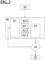
- An example of a method of operating an ion beam system with increased secondary electron yield is illustrated in Figure 3 .
- an inspection or repair site 41 is aligned at the optical axis of an ion beam system and an inspection or repair site is registered for example at semiconductor features or alignment fiducials present or generated at a wafer or mask surface.
- an inspection or repair task is specified.
- a repair task can for example comprise an editing operation of a semiconductor circuit at edit location 81 in a selected editing layer 75.E, such as a repair of a defect or a void (see figure 2 ).
- a CAD-information about the layer structure and the material compositions included in the multi-layer comprising layer 75.1 to 75.N of a semiconductor wafer 7 at the inspection or repair site 41 is received.
- Step M an ion beam image acquisition or sputtering is performed in step S1.
- the ion beam is scanned over the inspection or repair site 41 and, during scanning, secondary electrons are collected, and a layer of material is physically sputtered from the surface 15 of the sample 7. Secondary electrons are generated during ion beam scanning over the surface 15 and collected in step S3. Thereby, for example an image of the surface 15 of the sample 7 is generated.
- step S2.0 gases for increasing a secondary electron yield are selected.
- the selection is for example based on a known material composition of a sample, for example known from CAD data received during step S0.
- the selection is based on an analysis of an image of the surface 15, generated during ion beam scanning from the secondary electron signal collected during step S3.
- An image of the surface 15 is obtained by the secondary electron signal collected at each dwell point with the ion beam, wherein the secondary electron signal is generally depending on the material composition and topography at each dwell point.
- the different material compositions of semiconductor wafers or lithography masks is typically known, for example from received information during step S0.
- a gas selection for example to prevent a redeposition of sputtered material can be performed according to prior known material compositions.
- a gas selection for example to prevent a redeposition of sputtered material can be performed according to an analysis of an image collected from the surface 15 of the sample 7.
- a gas selection for example to change a work function of a material can be performed according to at least one of a prior known material composition or an analysis result of image collected from the surface 15 of the sample 7
- At least one selected gas is provided via one of the gas nozzles 635.1 to 635.3, each connected via a valve to a gas reservoir.
- a first gas 637.1 is provided via individual gas nozzle 635.1 to change a work function of a material comprised at the surface 15 of the sample 7 at the inspection site 41.
- a second gas 637.2 is provided via individual gas nozzle 635.2 to neutralize a surface charging of the sample 7 at the inspection site 41.
- a third gas 637.3 is provided to chemically remove sputtered material which has been physically sputtered during ion beam inspection or editing from the surface 15 of the sample 7.
- at least two of the first to third gases 637.1 to 637.3 are individually selected and provided to induce at least one of the desired effects, for example two effects in parallel.
- a combination of at least two gases is selected to enhance the secondary electron signal collected based on the inspection or repair task requirements.
- a repair task requires a precise end-pointing to stop an ion beam sputtering at a metal line and a certain suite of gases is selected and provided accordingly.
- a repair task requires to stop an ion beam sputtering at an insulating layer of for example SiO2, SiN2 or a low k dielectric.
- a composition of gases 637.1 to 637.3 provided by gas nozzles 635.1 to 635.3 is adjusted during ion beam scanning step S1 in dependence of an actual material composition of an actual layer 75.i reached during ion-beam scanning step S1.
- an actual material composition of an actual layer 75.i comprises a metal, such as copper or aluminum.
- a gas can be selected to trigger oxidation reactions on a metal, which may decrease the work function leading to more secondary electron emission during ion beam exposure in step S1.
- the crystal structure of metal surfaces can rearrange themselves to accommodate certain gases which are adsorbed. These adsorbates have their own coefficients of emission that may increase the SE signal generated at a metal structure during ion beam exposure in step S1.
- a gaseous vapor for example water vapor is introduced in the beam interaction region.
- a local surface temperature of a sample is lowered which has the effect of concentrating adsorbed gases for an increased adsorption and the effect of increased secondary electron yield.
- gas or combinations of gases may be chosen for insulating layers of for example layers comprising SiO2 or a low-k dielectrics as material compositions.
- gases that induce charge neutralization are more likely to have a positive effect on secondary electron collection.
- Gas mediated neutralization has the distinct advantage over other forms of charge neutralization, say for example an electron flood gun, of being able to dissipate charge even in high aspect ratio trenches.
- Table 1 Material composition First gas (Work function) Second gas (Charge neutralize) Third gas (Redeposition removal / passivation) Copper formic acid, nitro ethanol Xenon, Argon, Helium, Neon, Nitrogen, Krypton Xenon Difluoride Aluminum Hydrogen Peroxide Xenon, Argon, Helium, Neon, Nitrogen, Krypton Chlorine, Iodine, Bromine Insulator layer (SiN, SiO2) Methyl Nitro Acetate Xenon, Argon, Helium, Neon, Nitrogen, Krypton Xenon Difluoride, Oxygen Low-k dielectrics (SiOCH, porous SiO2, organo-silicate glass (OSG), carbon- doped oxide (CDO), fluorinated silicon glass (FSG), polymeric dielectrics Methyl Nitro Acetate Xenon, Argon, Helium, Neon, Nitrogen, Krypton water vapor Tungsten Hydro
- Some selected gases are specific for a selected material.
- water vapor can be selected as third gas for low-k dielectrics as well as first gas for copper
- Methyl nitro acetate can be selected as a first gas for low-k dielectrics.
- the at least two gases provided can be water vapor and Methyl nitro acetate. Thereby, secondary electron yield is increased and redeposition is reduced for both materials.
- step S2.0 different layers comprising different material compositions require different combinations of selected gases and a frequent adjustment of the selected gases in step S2.0, parallel to ion beam scanning step S1.
- the combination of selected gases in steps S2.1 to S2.3 is frequently adjusted, including an adjustment of a gas to ion flux ratio, beam current density, and gas replenishment time.
- the local gas flux selected by step S2.0 and provided by steps S2.1 to S2.3 can be tailored to maximize neutralization of positive or negative surface charges, while minimizing attenuation of the primary ion beam and secondary electrons escaping the surface.
- the combination of gases and beam can be alternatingly pulsed for more precise imaging control.
- Figure 4 illustrates an example of the effects during conventional ion beam inspection and milling with ion beam 103.
- the example shows a repair location 81 in a buried layer below a stack of alternating layers comprising structured layers 175 (with labels 175.1 ... 175.E provided to some layers) and isolating layers 177 (labels 177.1... 177.j provided to some examples).
- structured layers 175 with labels 175.1 ... 175.E provided to some layers
- isolating layers 177 labels 177.1... 177.j provided to some examples.
- a third group of secondary electrons 187 is generated inside layer 175.E, but unable to escape the layer 175.E due to surface charges 181, redeposited milling material 189.1 or a kinetic energy not sufficient to exit the layer 175.E.
- a first milled material layer 189.1 may be deposited on the interface of layer 175.E and a second milled material layer 189.2 may be deposited on the sidewalls of the deep trench 49 during ion beam milling.
- the actual milled or inspected layer 175.E of this example is shown as an structured layer 175.E, comprising both of conducting structures formed by a metal or doped silicon and isolating structures such as Silicon-Dioxide.
- Figure 5 illustrates the effects of the method according to the second embodiment.
- Figure 5a illustrates the effect of adding a second gas 637.2 of the group of SE-enhancement gases by the second nozzle 635.2 to the inspection site during ion beam inspection or milling.
- the second gas 637.2 By providing the second gas 637.2, charges sticking to exposed surfaces of isolators are removed or balanced, and secondary electrons are not attracted to exposed surfaces of isolators anymore (see reference number 647: an ion of a second gas molecule balances the residual charge captured at an isolating layer). Thereby, the secondary electron yield collected by detector 331 (see figure 1 ) is increased.
- the second gas can for example be Nitrogen gas comprising Nitrogen ions.
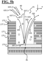
- Figure 5b illustrates the further effect of adding a third gas 637.3 of the group of SE-enhancement gases by the third nozzle 635.3 to the inspection site during ion beam inspection or milling.
- a third gas 637.3 redeposition of milled material is prevented and no layers of debris of milled material 189 (see figure 4 ) are built during ion beam inspection or milling. Thereby, for example an image generation or a milling operation is not deteriorated.
- the third gas can for example by Nitro ethanol or Xenon difluoride.
- Figure 5c illustrates the further effect of adding a first gas 637.1 of the first group of gases by the first nozzle 635.1 to the inspection site during ion beam inspection or milling.
- a first gas 637.1 By providing the first gas 637.1, a work function of a material is reduced, and a secondary electron yield is increased.
- a first gas 637.1 can for example be water vapor.
- a mixture of individual gases for increasing secondary electron yield according to the embodiment comprises at least two gases selected from the group of gases including first, second and third gases.
- the example of figure 5b with a second and third gas is one example, while other combinations of at least two gases comprising a first and second or first and third gas are possible as well.
- a secondary electron yield is increased by at least 15%.
- even higher secondary electron yield is achieved, for example with an increase of a secondary electron yield of more than 30%, or even more than 50%.
Landscapes
- Chemical & Material Sciences (AREA)
- Analytical Chemistry (AREA)
- Physics & Mathematics (AREA)
- Engineering & Computer Science (AREA)
- Plasma & Fusion (AREA)
- General Physics & Mathematics (AREA)
- Preparing Plates And Mask In Photomechanical Process (AREA)
- High Energy & Nuclear Physics (AREA)
Applications Claiming Priority (1)
| Application Number | Priority Date | Filing Date | Title |
|---|---|---|---|
| US18/456,309 US20250069956A1 (en) | 2023-08-25 | 2023-08-25 | Ion beam inspection and repair with increased secondary electron yield |
Publications (2)
| Publication Number | Publication Date |
|---|---|
| EP4513527A2 true EP4513527A2 (de) | 2025-02-26 |
| EP4513527A3 EP4513527A3 (de) | 2025-07-09 |
Family
ID=91585825
Family Applications (1)
| Application Number | Title | Priority Date | Filing Date |
|---|---|---|---|
| EP24182807.8A Pending EP4513527A3 (de) | 2023-08-25 | 2024-06-18 | Gasvermittelte sekundärelektronenerzeugung und sammlungsverstärkung für verbesserte endpunktdetektion mit edelionen zur schaltungsbearbeitung in halbleiterwafern |
Country Status (4)
| Country | Link |
|---|---|
| US (1) | US20250069956A1 (de) |
| EP (1) | EP4513527A3 (de) |
| KR (1) | KR20250030921A (de) |
| TW (1) | TWI902278B (de) |
Citations (2)
| Publication number | Priority date | Publication date | Assignee | Title |
|---|---|---|---|---|
| US8110114B2 (en) | 2004-03-26 | 2012-02-07 | Keenan Andrew D | Multiple filter controller and method of use |
| US9236225B2 (en) | 2003-10-16 | 2016-01-12 | Carl Zeiss Microscopy, Llc | Ion sources, systems and methods |
Family Cites Families (9)
| Publication number | Priority date | Publication date | Assignee | Title |
|---|---|---|---|---|
| US6987067B2 (en) * | 2002-08-21 | 2006-01-17 | International Business Machines Corporation | Semiconductor copper line cutting method |
| US6863787B2 (en) * | 2003-04-02 | 2005-03-08 | Fei Company | Dummy copper deprocessing |
| US7387738B2 (en) * | 2003-04-28 | 2008-06-17 | Air Products And Chemicals, Inc. | Removal of surface oxides by electron attachment for wafer bumping applications |
| WO2008005517A1 (en) * | 2006-07-07 | 2008-01-10 | Accretech Usa, Inc. | Processing chamber having labyrinth seal |
| DE102008040426B4 (de) * | 2008-07-15 | 2015-12-24 | Carl Zeiss Microscopy Gmbh | Verfahren zur Untersuchung einer Oberfläche eines Objekts |
| US9721754B2 (en) * | 2011-04-26 | 2017-08-01 | Carl Zeiss Smt Gmbh | Method and apparatus for processing a substrate with a focused particle beam |
| WO2016022427A2 (en) * | 2014-08-05 | 2016-02-11 | Tel Epion Inc. | Gcib nozzle assembly |
| KR101941867B1 (ko) * | 2015-08-20 | 2019-01-24 | 가부시키가이샤 히다치 하이테크놀로지즈 | 이온빔 장치 및 가스 전계 전리 이온원의 세정 방법 |
| KR20250105457A (ko) * | 2022-11-16 | 2025-07-08 | 칼 짜이스 에스엠테 게엠베하 | 깊은 다중층 구조의 개선된 편집 |
-
2023
- 2023-08-25 US US18/456,309 patent/US20250069956A1/en active Pending
-
2024
- 2024-05-31 TW TW113120160A patent/TWI902278B/zh active
- 2024-06-18 EP EP24182807.8A patent/EP4513527A3/de active Pending
- 2024-08-20 KR KR1020240111165A patent/KR20250030921A/ko active Pending
Patent Citations (2)
| Publication number | Priority date | Publication date | Assignee | Title |
|---|---|---|---|---|
| US9236225B2 (en) | 2003-10-16 | 2016-01-12 | Carl Zeiss Microscopy, Llc | Ion sources, systems and methods |
| US8110114B2 (en) | 2004-03-26 | 2012-02-07 | Keenan Andrew D | Multiple filter controller and method of use |
Also Published As
| Publication number | Publication date |
|---|---|
| TWI902278B (zh) | 2025-10-21 |
| TW202509989A (zh) | 2025-03-01 |
| EP4513527A3 (de) | 2025-07-09 |
| KR20250030921A (ko) | 2025-03-05 |
| US20250069956A1 (en) | 2025-02-27 |
Similar Documents
| Publication | Publication Date | Title |
|---|---|---|
| US8303833B2 (en) | High resolution plasma etch | |
| US6753538B2 (en) | Electron beam processing | |
| EP1710327B1 (de) | Strahleninduziertes Verfahren zum selektiven Ätzen eines Material aus einem Quarzsubstrat | |
| JP5090255B2 (ja) | 原位置でのstemサンプル作製方法 | |
| JP5600371B2 (ja) | 荷電粒子ビーム処理のための保護層のスパッタリング・コーティング | |
| US20110163068A1 (en) | Multibeam System | |
| US7256405B2 (en) | Sample repairing apparatus, a sample repairing method and a device manufacturing method using the same method | |
| Wanzenboeck et al. | Focused ion beam lithography | |
| US20250266240A1 (en) | Editing of deep, multi-layered structures | |
| Prewett | Focused ion beams—microfabrication methods and applications | |
| US10347463B2 (en) | Enhanced charged particle beam processes for carbon removal | |
| EP4513527A2 (de) | Gasvermittelte sekundärelektronenerzeugung und sammlungsverstärkung für verbesserte endpunktdetektion mit edelionen zur schaltungsbearbeitung in halbleiterwafern | |
| JPH08222175A (ja) | 荷電粒子を用いた微細加工方法及び装置 | |
| Cui | Nanofabrication by Focused Ion Beam | |
| Brown | Applications of Ion Beams in Microlithography | |
| KR20260026569A (ko) | 3d 단층촬영 동안의 전하 보상을 위한 개선된 방법 및 장치 | |
| Melngailis | Applications of ion microbeams lithography and direct processing | |
| Harriott | Ion Beam Techniques and Applications | |
| Cui | Nanofabrication by Ion Beam | |
| Prewett | Focused Ion Beams and their Applications in Microfabrication | |
| BROWN | Bell Laboratories, 600 Mountain Avenue, Murrey Hill, New Jersey 07974, USA | |
| PREWETT | CHILTON, DIDCOT OXFORDSHIRE OX11 OQX | |
| Yasaka | Feasibility study of spatial-phase-locked focused-ion-beam lithography | |
| Radelaar | Technology and fabrication of quantum devices: Submicron lithography and etching techniques | |
| Tseng | Fabrication of nanoscale structures using ion beams |
Legal Events
| Date | Code | Title | Description |
|---|---|---|---|
| PUAI | Public reference made under article 153(3) epc to a published international application that has entered the european phase |
Free format text: ORIGINAL CODE: 0009012 |
|
| STAA | Information on the status of an ep patent application or granted ep patent |
Free format text: STATUS: THE APPLICATION HAS BEEN PUBLISHED |
|
| AK | Designated contracting states |
Kind code of ref document: A2 Designated state(s): AL AT BE BG CH CY CZ DE DK EE ES FI FR GB GR HR HU IE IS IT LI LT LU LV MC ME MK MT NL NO PL PT RO RS SE SI SK SM TR |
|
| PUAL | Search report despatched |
Free format text: ORIGINAL CODE: 0009013 |
|
| AK | Designated contracting states |
Kind code of ref document: A3 Designated state(s): AL AT BE BG CH CY CZ DE DK EE ES FI FR GB GR HR HU IE IS IT LI LT LU LV MC ME MK MT NL NO PL PT RO RS SE SI SK SM TR |
|
| RIC1 | Information provided on ipc code assigned before grant |
Ipc: G03F 1/78 20120101ALI20250602BHEP Ipc: G03F 1/74 20120101ALI20250602BHEP Ipc: H01L 21/768 20060101ALI20250602BHEP Ipc: H01J 37/02 20060101ALI20250602BHEP Ipc: H01J 37/317 20060101ALI20250602BHEP Ipc: H01J 37/305 20060101AFI20250602BHEP |
|
| STAA | Information on the status of an ep patent application or granted ep patent |
Free format text: STATUS: THE APPLICATION IS DEEMED TO BE WITHDRAWN |