EP4513883A1 - Kameraanordnung, herstellungsverfahren für kameraanordnung und elektronische vorrichtung - Google Patents
Kameraanordnung, herstellungsverfahren für kameraanordnung und elektronische vorrichtung Download PDFInfo
- Publication number
- EP4513883A1 EP4513883A1 EP23811118.1A EP23811118A EP4513883A1 EP 4513883 A1 EP4513883 A1 EP 4513883A1 EP 23811118 A EP23811118 A EP 23811118A EP 4513883 A1 EP4513883 A1 EP 4513883A1
- Authority
- EP
- European Patent Office
- Prior art keywords
- circuit board
- camera assembly
- hollow portion
- package body
- board
- Prior art date
- Legal status (The legal status is an assumption and is not a legal conclusion. Google has not performed a legal analysis and makes no representation as to the accuracy of the status listed.)
- Pending
Links
Images



Classifications
-
- H—ELECTRICITY
- H10—SEMICONDUCTOR DEVICES; ELECTRIC SOLID-STATE DEVICES NOT OTHERWISE PROVIDED FOR
- H10F—INORGANIC SEMICONDUCTOR DEVICES SENSITIVE TO INFRARED RADIATION, LIGHT, ELECTROMAGNETIC RADIATION OF SHORTER WAVELENGTH OR CORPUSCULAR RADIATION
- H10F39/00—Integrated devices, or assemblies of multiple devices, comprising at least one element covered by group H10F30/00, e.g. radiation detectors comprising photodiode arrays
- H10F39/80—Constructional details of image sensors
- H10F39/804—Containers or encapsulations
-
- G—PHYSICS
- G06—COMPUTING OR CALCULATING; COUNTING
- G06F—ELECTRIC DIGITAL DATA PROCESSING
- G06F1/00—Details not covered by groups G06F3/00 - G06F13/00 and G06F21/00
- G06F1/16—Constructional details or arrangements
- G06F1/1613—Constructional details or arrangements for portable computers
- G06F1/1615—Constructional details or arrangements for portable computers with several enclosures having relative motions, each enclosure supporting at least one I/O or computing function
- G06F1/1616—Constructional details or arrangements for portable computers with several enclosures having relative motions, each enclosure supporting at least one I/O or computing function with folding flat displays, e.g. laptop computers or notebooks having a clamshell configuration, with body parts pivoting to an open position around an axis parallel to the plane they define in closed position
-
- G—PHYSICS
- G06—COMPUTING OR CALCULATING; COUNTING
- G06F—ELECTRIC DIGITAL DATA PROCESSING
- G06F1/00—Details not covered by groups G06F3/00 - G06F13/00 and G06F21/00
- G06F1/16—Constructional details or arrangements
- G06F1/1613—Constructional details or arrangements for portable computers
- G06F1/1633—Constructional details or arrangements of portable computers not specific to the type of enclosures covered by groups G06F1/1615 - G06F1/1626
- G06F1/1684—Constructional details or arrangements related to integrated I/O peripherals not covered by groups G06F1/1635 - G06F1/1675
- G06F1/1686—Constructional details or arrangements related to integrated I/O peripherals not covered by groups G06F1/1635 - G06F1/1675 the I/O peripheral being an integrated camera
-
- H—ELECTRICITY
- H04—ELECTRIC COMMUNICATION TECHNIQUE
- H04M—TELEPHONIC COMMUNICATION
- H04M1/00—Substation equipment, e.g. for use by subscribers
- H04M1/02—Constructional features of telephone sets
- H04M1/0202—Portable telephone sets, e.g. cordless phones, mobile phones or bar type handsets
- H04M1/026—Details of the structure or mounting of specific components
- H04M1/0264—Details of the structure or mounting of specific components for a camera module assembly
-
- H—ELECTRICITY
- H04—ELECTRIC COMMUNICATION TECHNIQUE
- H04N—PICTORIAL COMMUNICATION, e.g. TELEVISION
- H04N23/00—Cameras or camera modules comprising electronic image sensors; Control thereof
- H04N23/50—Constructional details
- H04N23/54—Mounting of pick-up tubes, electronic image sensors, deviation or focusing coils
-
- H—ELECTRICITY
- H04—ELECTRIC COMMUNICATION TECHNIQUE
- H04N—PICTORIAL COMMUNICATION, e.g. TELEVISION
- H04N23/00—Cameras or camera modules comprising electronic image sensors; Control thereof
- H04N23/50—Constructional details
- H04N23/55—Optical parts specially adapted for electronic image sensors; Mounting thereof
-
- H—ELECTRICITY
- H04—ELECTRIC COMMUNICATION TECHNIQUE
- H04N—PICTORIAL COMMUNICATION, e.g. TELEVISION
- H04N23/00—Cameras or camera modules comprising electronic image sensors; Control thereof
- H04N23/57—Mechanical or electrical details of cameras or camera modules specially adapted for being embedded in other devices
-
- H—ELECTRICITY
- H10—SEMICONDUCTOR DEVICES; ELECTRIC SOLID-STATE DEVICES NOT OTHERWISE PROVIDED FOR
- H10F—INORGANIC SEMICONDUCTOR DEVICES SENSITIVE TO INFRARED RADIATION, LIGHT, ELECTROMAGNETIC RADIATION OF SHORTER WAVELENGTH OR CORPUSCULAR RADIATION
- H10F39/00—Integrated devices, or assemblies of multiple devices, comprising at least one element covered by group H10F30/00, e.g. radiation detectors comprising photodiode arrays
- H10F39/011—Manufacture or treatment of image sensors covered by group H10F39/12
-
- H—ELECTRICITY
- H10—SEMICONDUCTOR DEVICES; ELECTRIC SOLID-STATE DEVICES NOT OTHERWISE PROVIDED FOR
- H10F—INORGANIC SEMICONDUCTOR DEVICES SENSITIVE TO INFRARED RADIATION, LIGHT, ELECTROMAGNETIC RADIATION OF SHORTER WAVELENGTH OR CORPUSCULAR RADIATION
- H10F39/00—Integrated devices, or assemblies of multiple devices, comprising at least one element covered by group H10F30/00, e.g. radiation detectors comprising photodiode arrays
- H10F39/80—Constructional details of image sensors
- H10F39/806—Optical elements or arrangements associated with the image sensors
-
- H—ELECTRICITY
- H10—SEMICONDUCTOR DEVICES; ELECTRIC SOLID-STATE DEVICES NOT OTHERWISE PROVIDED FOR
- H10F—INORGANIC SEMICONDUCTOR DEVICES SENSITIVE TO INFRARED RADIATION, LIGHT, ELECTROMAGNETIC RADIATION OF SHORTER WAVELENGTH OR CORPUSCULAR RADIATION
- H10F39/00—Integrated devices, or assemblies of multiple devices, comprising at least one element covered by group H10F30/00, e.g. radiation detectors comprising photodiode arrays
- H10F39/80—Constructional details of image sensors
- H10F39/811—Interconnections
Definitions
- This application relates to the field of electronic device technologies, and in particular, to a camera assembly, a camera assembly preparation method, and an electronic device.
- a form of an electronic device gradually develops towards a direction of lightness and thinness or a high screen-to-body ratio.
- a camera assembly can implement an image capturing function.
- at least one camera assembly is usually configured.
- a conventional camera assembly imposes a clear constraint on lightness and thinness and high screen-to-body ratio design of the notebook computer due to large space occupation.
- a thickness size of the notebook computer is large.
- a width size of the camera assembly is large, large occupied space is increased, which is not conducive to improving a screen-to-body ratio of a display.
- This application provides a camera assembly that helps reduce space occupation, a camera assembly preparation method, and an electronic device.
- this application provides a camera assembly, which may include a circuit board, a photosensitive chip, a package body, and a camera lens.
- the circuit board has a hollow portion.
- the photosensitive chip is electrically connected to the circuit board, and is fastened in the hollow portion by using the package body.
- the package body has a first mounting surface. One end of the camera lens faces the photosensitive chip and is fixedly attached to the first mounting surface.
- the hollow portion is provided in the circuit board, and the photosensitive chip is disposed in the hollow portion, which helps reduce a height size of the camera assembly.
- the camera lens is fastened to the circuit board by using the package body, which further helps reduce a width size of the camera assembly, helps implement a miniaturization and lightness and thinness design of the camera assembly, and can reduce space occupation of the camera assembly.
- the circuit board may be of a long strip structure. That is, a length size of the circuit board is greater than a width size of the circuit board.
- the width size of the circuit board may be the same as a width size of the camera lens, so that the width size of the camera assembly is reduced.
- the camera assembly may further include a light filter.
- the package body may further have a second mounting surface, and the light filter may be fastened to the second mounting surface.
- the package body may further include a light-filtering material, and the package body may cover a light-receiving surface of the photosensitive chip. That is, the package body may function as a light filter. Therefore, during actual application, disposing of the light filter may be omitted, which helps reduce a quantity of components of the camera assembly, and can reduce preparation difficulty and costs of the camera assembly.
- a part of the package body may be located outside the hollow portion.
- the first mounting surface may be located on a surface that is of the package body and that faces away from the circuit board.
- the second mounting surface may be located on a surface that is of the package body and that faces away from the circuit board.
- the surface facing away from the circuit board may be a step surface.
- a distance between the first mounting surface and the circuit board may be greater than a distance between the second mounting surface and the circuit board. That is, the first mounting surface is farther away from the circuit board than the second mounting surface.
- the hollow portion may be a groove, or may be a through hole. That is, the hollow portion may penetrate a thickness of the circuit board, or may not penetrate a thickness of the circuit board.
- a pad of the circuit board may be located on a bottom wall of the groove. After the photosensitive chip is disposed in the hollow portion, an electrical connection between the photosensitive chip and the circuit board may be implemented. Certainly, the pad may alternatively be located on a first board surface of the circuit board or in another position. Details are not described herein.
- the pad of the circuit board may be located on the first board surface.
- the photosensitive chip and the circuit board may be connected through a connection line. That is, one end of the connection line may be connected to the pad, and the other end of the connection line may be connected to the photosensitive chip.
- the package body may alternatively package the connection line. That is, the connection line may be wrapped in the package body, so that the package body protects the connection line.
- a sink may be further provided on the first board surface of the circuit board, the hollow portion may be located in the sink, and the pad of the circuit board may be located on an inner wall of the sink.
- the sink is provided, and the pad is disposed on the inner wall of the sink, which helps reduce a height of the connection line, and can prevent the connection line from being scratched, so that safety of the connection line can be improved. In addition, this also helps reduce the height size of the camera assembly.
- the package body When the package body is specifically disposed, the package body may fill the hollow portion, to ensure connection strength between the photosensitive chip and the circuit board, and improve structural strength of the circuit board.
- the camera assembly may further include a support board.
- the support board may be disposed on a second board surface (a surface facing away from the first board surface) of the circuit board, and is fastened to the circuit board. Disposing the support board can improve structural strength of the circuit board.
- this application further provides a camera assembly preparation method.
- the method may include:
- connection rib is disposed between the circuit boards, which helps ensure connection strength between adjacent circuit boards.
- connection strength between adjacent circuit boards.
- specific structural strength can be maintained.
- a support board may be further disposed on a second board surface of the circuit board, to improve structural strength of the circuit board.
- the support board may be included, or the support board may be removed.
- a light filter may be fastened to the package body.
- a camera lens may be connected to the package body, to avoid using a structure such as a support, which helps reduce a size of the camera assembly.
- this application further provides an electronic device.
- the electronic device may include the foregoing camera assembly or a camera assembly obtained by using the foregoing preparation method.
- the electronic device may include a housing, and the camera assembly may be disposed in the housing.
- the electronic device may be specifically a notebook computer, a tablet computer, a television, a smartwatch, or the like. A specific type of the electronic device is not limited in this application.
- the camera assembly provided in this application facilitates a miniaturization and lightness and thinness design of the electronic device.
- FIG. 1 is a diagram of a three-dimensional structure of a notebook computer according to an embodiment of this application.
- the notebook computer may include a system end 01 and a display end 02.
- the system end 01 and the display end 02 may be connected by using a structure such as a hinge (not shown in the figure), so that the system end 01 and the display end 02 can be opened or closed relative to each other, to implement a foldable function of the notebook computer.
- the system end 01 may usually include a bottom housing 011, a keyboard 012, a touchpad 013, and components such as a mainboard, a processor, and a battery located in the bottom housing 011.
- the display end 02 may usually include components such as an upper cover 021 and a display 022.
- a camera assembly 10 may be disposed at the display end 02. During specific disposition, the camera assembly 10 may be disposed in a frame 023 of the upper cover 021.
- the frame 023 may provide abundant mounting space for the camera assembly 10, and can well protect the camera assembly 10.
- the user may adjust a direction of the camera assembly 10 by adjusting an orientation of the display end 02, to obtain a required visual angle for image shooting. Therefore, flexible use experience is provided.
- a plane on which the display 022 is located may also be referred to as a surface B, and a screen-to-body ratio of the display 022 is a ratio of a display region of the display 022 to the surface B.
- a value of a width size d1 of the frame 023 is usually reduced.
- the camera assembly 10 is disposed in the frame 023, and the width size d1 of the frame 023 is usually greater than a width size of the camera assembly 10.
- the width size of the camera assembly 10 imposes a constraint on the width size d1 of the frame 023, and affects further narrowing of the frame 023. Therefore, reducing the width size of the camera assembly 10 helps improve the screen-to-body ratio of the display 022.
- the camera assembly 10 provided in embodiments of this application may alternatively be used in an electronic device such as a tablet computer, a television, or a smartwatch, to implement an image shooting function.
- an electronic device such as a tablet computer, a television, or a smartwatch.
- a specific application scenario of the camera assembly 10 is not limited in this application.
- FIG. 2 is a top view of a conventional camera assembly 03 according to this application
- FIG. 3 is a sectional view in an A-A direction of FIG. 2 .
- the camera assembly 03 may include a circuit board 031, a photosensitive chip 032, a light filter 033, and a camera lens 034 that are sequentially disposed in a stacked manner.
- the camera lens 034 is fastened to the circuit board 031 by using a support 035.
- a width size d2 of the support 035 is usually large, and is greater than a width size of the camera lens 034, which consequently increases a width size of the camera assembly 03.
- the support 035 is connected to the circuit board 031. Therefore, the circuit board 031 needs to have an abundant width size for mounting the support 035, which consequently increases the width size of the circuit board 031.
- the width size of the circuit board 031 is not less than the width size d2 of the support 035.
- a height size h of the camera assembly 03 is usually large.
- the camera lens 034 and the light filter 033 are connected to the circuit board 031 by using the support 035, which further increases the height size h of the camera assembly 03.
- this application provides a camera assembly that helps implement a miniaturization and lightness and thinness design.
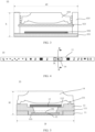
- the camera assembly 10 may include a circuit board 11, a photosensitive chip 12, a package body 13, and a camera lens 14.
- the circuit board 11 has a first board surface 111 (an upper board surface in FIG. 5 ), and the first board surface 111 has a hollow portion 110 (a dashed box in FIG. 5 ).
- the photosensitive chip 12 is electrically connected to the circuit board 11, and is fastened in the hollow portion 110 by using the package body 13.
- the package body 13 has a first mounting surface 131.
- One end of the camera lens 14 faces the photosensitive chip 12 and is fixedly attached to the first mounting surface 131.
- the hollow portion 110 is provided in the circuit board 11, and the photosensitive chip 12 is disposed in the hollow portion 110, which helps reduce a height size H of the camera assembly 10.
- the camera lens 14 is fastened to the circuit board 11 by using the package body 13, which further reduces a width size D of the camera assembly 10.
- the width sizes of the camera assembly 03 and the circuit board 031 are approximately equal to the width size d2 of the support 035, and are greater than the width size of the camera lens 034.
- the support 035 in FIG. 3 is omitted, width sizes of the camera assembly 10 and the circuit board 11 are approximately equal to a width size of the camera lens 14. Therefore, a first mounting surface 131 is provided on the package body 13, so that a fixed connection between the camera lens 14 and the circuit board 11 can be implemented, and disposing of the support 035 can be omitted, which helps reduce the width size D of the camera assembly 10.
- the camera lens 034 needs to be fastened to the circuit board 031 by using the support 035, to ensure a minimum distance between the camera lens 034 and the photosensitive chip 032, and implement a fixed connection between the camera lens 034 and the circuit board 031.
- the first mounting surface 131 is provided on the package body 13, so that a fixed connection between the package body 13 and the camera lens 14 can be implemented.
- a distance between the first mounting surface 131 and the circuit board 11 (or the photosensitive chip 12) is properly set, so that a minimum distance between the camera lens 14 and the photosensitive chip 12 can be ensured.
- a part of the package body 13 may extend out of the hollow portion 110.
- the first mounting surface 131 may be located on a surface that is of the package body 13 and that faces away from the circuit board 11. A length, of the package body 13, extending out of the hollow portion 110 is controlled, so that the distance between the first mounting surface 131 and the circuit board 11 can be effectively controlled.
- the package body 13 is disposed, so that a fixed connection between the photosensitive chip 12, the camera lens 14, and the circuit board 11 can be implemented, and position progress between the photosensitive chip 12 and the camera lens 14 can be effectively controlled, which helps ensure quality of the camera assembly 10.
- the circuit board 11 is of a long strip shape. That is, the width size of the circuit board 11 is smaller, and a length size of the circuit board 11 is larger.
- the long strip-shaped circuit board 11 can provide a board surface of a larger area in a limited width size, and can be configured to provide a larger board layout area for an electrical element.
- a gap between the photosensitive chip 12 and the circuit board 11 can be further filled, which helps improve structural strength of the circuit board 11 and ensures structural safety of the camera assembly 03.
- FIG. 6 is a brief diagram of a cross-sectional structure of a camera lens 14 according to an embodiment of this application.
- the camera lens 14 may include a lens cone 141 and a plurality of lenses 142 (five lenses are shown in FIG. 6 ) located in the lens cone 141.
- the plurality of lenses 142 may include a flat lens, a convex lens, a concave lens, and the like.
- a quantity, disposing positions, and shapes of the lenses 142 are not limited in this application.
- a main function of the lens cone 141 is to provide a mounting position for the lens 142, and form the plurality of lenses 142 into an integrated structure.
- the lens cone 141 may be of a tubular structure with openings at two ends.
- a sectional shape of the lens cone 141 may be a circle, a rectangle, an ellipse, an irregular shape, or the like.
- Light may enter the camera lens 14 from one end of the lens cone 141, and is emitted inward from the other end of the lens cone 141 after being processed by the lens 142 in the lens cone 141.
- the camera lens 14 may alternatively include a structural part such as a protective housing or a shielding can.
- a specific structure of the camera lens 14 is not limited in this application.
- one end of the lens cone 141 may be coated with glue 143, and then the end coated with the glue 143 is directly attached to the first mounting surface 131. After the glue 143 is solidified, a fixed connection between the camera lens 14 and the package body 13 may be implemented.
- the camera lens 14 may be fastened to the package body 13 through a welding technology or the like.
- a manner of connecting the camera lens 14 to the package body 13 is not limited in this application.
- the circuit board 11 may be a printed circuit board (Printed Circuit Board, PCB), a flexible circuit board (Flexible Printed Circuit, FPC), or the like.
- the circuit board 11 may be a single-layer board or a multilayer board. A specific type of the circuit board 11 is not limited in this application.
- the photosensitive chip 12 is a component for converting an optical image into an electrical signal.
- an optical signal may be converted into an electrical signal.
- the light-receiving surface 120 may specifically include a charge-coupled device (Charge-coupled Device, CCD), a complementary metal oxide semiconductor (Complementary Metal Oxide Semiconductor, CMOS), and the like.
- CCD Charge-coupled Device
- CMOS complementary metal oxide semiconductor
- CMOS complementary Metal Oxide Semiconductor
- the camera assembly 10 may further include a light filter 15.
- the light filter 15 may be an infrared light filter 15. That is, the light filter 15 may effectively filter infrared light in a specific band, to weaken infrared light transmitted to the photosensitive chip 12.
- a specific type of the light filter 15 is not limited in this application.
- the package body 13 further has a second mounting surface 132, and the light filter 15 may be fastened to the second mounting surface 132.
- a surface that is of the light filter 15 and that faces the second mounting surface 132 may be coated with glue, and then the surface coated with the glue is directly attached to the second mounting surface 132. After the glue is solidified, a fixed connection between the camera lens 14 and the package body 13 may be implemented.
- the light filter 15 may alternatively be fastened to the package body 13 through a welding technology or the like. A manner of connecting the light filter 15 to the package body 13 is not specifically limited in this application.
- the part of the package body 13 may extend out of the hollow portion 110.
- the second mounting surface 132 may be located on the surface that is of the package body 13 and that faces away from the circuit board 11.
- the surface that is of the package body 13 and that faces away from the circuit board 11 may be a step surface.
- the distance between the first mounting surface 131 and the circuit board 11 may be greater than a distance between the second mounting surface 132 and the circuit board 11. That is, the first mounting surface 131 is farther away from the circuit board than the second mounting surface 132, so that the light filter 15 is disposed between the camera lens 14 and the photosensitive chip 12.
- a height difference between the first mounting surface 131 and the second mounting surface 132 may be properly set according to an actual requirement (for example, a thickness size of the light filter 15). Details are not described herein.
- the first mounting surface 131 and the second mounting surface 132 may be prepared together according to an actual size requirement.
- the photosensitive chip 12 may be first packaged, and then the formed package body 13 is stacked, cut, or ground, to prepare the first mounting surface 131 and the second mounting surface 132.
- the photosensitive chip 12, the camera lens 14, and the light filter 15 may all be fastened to the circuit board 11 by using the package body 13, which can effectively simplify a preparation procedure, to facilitate improvement of preparation efficiency.
- introduction of an additional support structure can be further avoided, which helps implement a lightweight and miniaturization design of the camera assembly 10.
- a material of the package body 13 may be ceramic, silicon dioxide, polymer, or the like. During specific application, the material and a preparation technology of the package body 13 may be properly selected and adjusted according to an actual requirement. Details are not described herein.
- a specific structure of the hollow portion 110 may be diversified.
- the hollow portion 110 may be a through hole. That is, the hollow portion 110 penetrates the first board surface 111 and the second board surface 112 of the circuit board 11.
- the first board surface 111 and the second board surface 112 are board surfaces that are of the circuit board 11 and that face away from each other.
- a distance L1 between one side edge of the hollow portion 110 and one side edge of the circuit board 11 may range from 0.2 mm to 2 mm.
- a distance L2 between another side edge of the hollow portion 110 and another side edge of the circuit board 11 may range from 0.2 mm to 2 mm.
- L1 and L2 may be equal, or may be unequal. Alternatively, in another implementation, L1 may be zero. Alternatively, L2 may be zero.
- connection line 16 may be electrically connected through a connection line 16.
- a pad 113 may be disposed on the first board surface 111 of the circuit board 11.
- One end of the connection line 16 (which may also be referred to as a gold wire) may be welded to the pad 113 of the circuit board 11, and the other end of the connection line 16 is welded to a pin of the photosensitive chip 12, to implement an electrical connection between the photosensitive chip 12 and the circuit board 11.
- the first board surface 111 has a sink 114.
- the hollow portion 110 is located in the sink 114, and the pad 113 is located on an inner wall of the sink 114.
- the hollow portion 110 is of a through-hole structure.
- the hollow portion 110 is provided on a bottom wall of the sink 114 and penetrates a thickness of the sink 114, and the pad 113 is located on the bottom wall of the sink 114.
- the sink 114 is provided, and the pad 113 is disposed on the bottom wall of the sink 114, which helps reduce a height of the connection line 16, and can prevent the connection line 16 from being scratched, so that safety of the connection line 16 can be improved. In addition, this also helps reduce the height size of the camera assembly 10.
- a thickness size of the bottom wall of the sink 114 may be the same as or different from a thickness size of the photosensitive chip 12. This is not specifically limited in this application.
- the pad 113 may be disposed on a side wall of the sink 114, which can also reduce the height of the gold wire. Details are not described herein again.
- the camera assembly 10 may further include a support board 17.
- the support board 17 is disposed on the second board surface 112 of the circuit board 11, and is fastened to the circuit board 11. Disposing the support board 17 can improve structural strength of the circuit board 11. When the circuit board 11 is subject to an external force, the support board 17 can effectively disperse the external force, to reduce an acting force the circuit board 11 is subject to, and prevent the circuit board 11 from being bent, broken, or the like.
- the photosensitive chip 12 may alternatively be attached and fastened to the support board 17, so that connection stability between the photosensitive chip 12 and the circuit board 11 can be improved.
- disposing the support board 17 further helps ensure position precision between the photosensitive chip 12 and the circuit board 11.
- the support board 17 may be attached to the second board surface 112 of the circuit board 11.
- the photosensitive chip 12 is disposed in the hollow portion 110, and the photosensitive chip 12 is attached to the support board 17, so that a back surface (a surface facing away from the light-receiving surface 120) of the photosensitive chip 12 can be kept flush with the second board surface 112 of the substrate, to improve relative position precision between the photosensitive chip 12 and the circuit board 11.
- rigidity of the support board 17 may be greater than, equal to, or less than rigidity of the circuit board 11.
- the support board 17 may be of a board structure with a clear thickness, or may be of a film structure with a small thickness, or the like. A material and a specific size of the support board 17 are not limited in this application.
- the support board 17 may be disposed on the second board surface 112 of the circuit board 11, to prevent the circuit board 11 from being bent, broken, or the like. After preparation of the package body 13 is completed, the support board 17 may be removed, to prevent the support board 17 from increasing the height size of the camera assembly 10.
- the support board 17 may alternatively not be removed, so that structural safety of the circuit board 11 can be ensured.
- the hollow portion 110 may alternatively be a groove. That is, the hollow portion 110 does not penetrate the second board surface 112 of the circuit board 11.
- the pad 113 may be located on the first board surface 111 of the circuit board 11, and the photosensitive chip 12 and the circuit board 11 may be electrically connected through the connection line 16.
- the pad 113 may be located on a bottom wall of the groove.
- a surface-mount technology or the like may be used to implement the electrical connection between the photosensitive chip 12 and the circuit board 11.
- a depth size of the groove may be greater than a height size of the photosensitive chip 12. That is, the photosensitive chip 12 does not extend out of the groove.
- a depth size of the groove may be less than a height size of the photosensitive chip 12. That is, the photosensitive chip 12 may extend out of the groove.
- a depth size of the groove may alternatively be approximately the same as a height size of the photosensitive chip 12. Details are not described herein.
- a specific structure of the package body 13 may also be diversified.
- the package body 13 may be filled between a side wall of the photosensitive chip 12 and a side wall of the hollow portion 110.
- the package body 13 may package the connection line 16.
- the connection line 16 may be wrapped in the package body 13, so that the package body 13 protects the connection line 16.
- the package body 13 may be located on the first board surface 111 of the circuit board 11.
- the package body 13 may cover the light-receiving surface 120 of the photosensitive chip 12, so that protection of the photosensitive chip 12 can be enhanced, and in addition, connection stability between the photosensitive chip 12 and the circuit board 11 can be improved.
- the package body 13 may be made of a material with good light transmission, to prevent the package body 13 from adversely affecting working performance of the photosensitive chip 12.
- the package body 13 may have a light-filtering material.
- the package body 13 may effectively filter light in a specific band.
- the package body 13 may function as a light filter. Therefore, during actual application, disposing of the light filter may be omitted, which helps reduce a quantity of components of the camera assembly 10, and can reduce preparation difficulty and costs of the camera assembly 10.
- an embodiment of this application further provides a camera assembly preparation method.
- the method may include the following steps.
- Step S100 Provide a circuit board assembly.
- the circuit board assembly includes at least two circuit boards that are disposed in a flat manner in a first direction, and a connection rib exits between two adjacent circuit boards.
- Step S200 Provide a hollow portion on a first board surface of the circuit board.
- a projection of the hollow portion is within the connection rib.
- Step S300 Dispose a photosensitive chip in the hollow portion, and electrically connect the photosensitive chip to the circuit board.
- Step S400 Package the photosensitive chip in the hollow portion by using a package body.
- Step S500 Remove the connection rib.
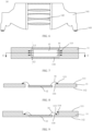
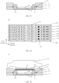
- the circuit board assembly 20 includes six circuit boards that are sequentially arranged in the first direction, which are a circuit board 11a, a circuit board 11b, a circuit board 11c, a circuit board 11d, a circuit board 11e, and a circuit board 11f.
- adjacent circuit boards are connected by using the connection rib, so that the plurality of circuit boards can be connected to form an integrated structure, to facilitate transportation or another subsequent preparation procedure.
- the circuit board 11a and the circuit board 11b are connected by using a connection rib 21b
- the circuit board 11b and the circuit board 11c are connected by using a connection rib 21c
- the circuit board 11c and the circuit board 11d are connected by using a connection rib 21d
- the circuit board 11d and the circuit board 11e are connected by using a connection rib 21e
- the circuit board 11e and the circuit board 11f are connected by using a connection rib 21f.
- a protection strip 22a and a protection strip 22b are disposed on two sides of the circuit board assembly 20.
- a connection rib 21a is disposed between the protection strip 22a and the circuit board 11a, and the protection strip 22b and the circuit board 11f are also connected by using a connection rib 21g.
- a preparation device for example, a mechanical arm
- disposing of the protection strip may alternatively be omitted.
- a plurality of auxiliary ribs 23 are also shown. These ribs 23 help ensure connection stability between two adjacent circuit boards. During actual application, the rib 23 only needs to ensure connection stability between two adjacent circuit boards, or connection stability between the circuit board and the protection strip. That is, in a second direction, a size of the rib 23 may be less than a size of the connection rib (for example, the connection rib 21a), so that the rib 23 is cut subsequently. During actual application, a disposing quantity and positions of the ribs 23 may be properly set according to an actual requirement. This is not limited in this application.
- a gap between two adjacent circuit boards may be provided by a manufacturer of the circuit board. That is, the gap between two adjacent circuit boards may be prepared by the manufacturer of the circuit board, to reduce subsequent cutting time.
- circuit board assembly 20 may alternatively include two, three, or more circuit boards.
- a specific quantity of circuit boards is not limited in this application.
- a hollow portion 110a may be provided in the circuit board 11a
- a hollow portion 110b may be provided in the circuit board 11b
- a hollow portion 110c may be provided in the circuit board 11c
- a hollow portion 110d may be provided in the circuit board 11d
- a hollow portion 110e may be provided in the circuit board 11e
- a hollow portion 110f may be provided in the circuit board 11f.
- a projection of the hollow portion is within the connection rib.
- the hollow portion 110a and the connection rib 21a are used as examples.
- a projection of the hollow portion 110a is within the connection rib 21a.
- connection parts between the circuit board 11a and the connection rib 21a there are still abundant connection parts between the circuit board 11a and the connection rib 21a, so that an adverse situation such as a break of the circuit board 11a can be prevented.
- a width size L3 between a side edge of the hollow portion 110a and a side edge of the circuit board 11 is small (for example, less than 2 mm). Therefore, there is no abundant material to ensure structural strength of the circuit board 11a.
- an adverse situation such as a break is prone to occurring, which affects smooth performance of a subsequent preparation procedure and reduces preparation quality of a camera assembly.
- connection rib that is, a size of the connection rib in the second direction
- a length of the connection rib may be properly set based on an actual size of the hollow portion. Details are not described herein.
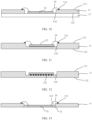
- the method may further include: disposing a support board 17 on a second board surface 112 of a circuit board 11.
- a first board surface 111 faces away from the second board surface 112. Disposing the support board 17 can improve structural strength of the circuit board 11 (or the circuit board assembly 20).
- the support board 17 can effectively disperse the external force, to reduce an acting force the circuit board 11 is subject to, and prevent the circuit board 11 from being bent, broken, or the like.
- a photosensitive chip 12 and the circuit board 11 may be electrically connected through a connection line 16 (or a gold wire).
- a connection line 16 (or a gold wire).
- one end of the connection line 16 may be welded to a pad 113 of the circuit board 11, and the other end of the connection line 16 may be welded to a pin of the photosensitive chip 12, to implement an electrical connection between the photosensitive chip 12 and the circuit board 11.
- the photosensitive chip 12 and the circuit board 11 may alternatively be electrically connected by using a surface-mount technology or the like.
- a specific manner of implementing the electrical connection between the photosensitive chip 12 and the circuit board 11 is not limited in this application.
- the packaging material when the photosensitive chip 12 is packaged, ceramic, silicon dioxide, polymer, or the like may be used as a packaging material. After the packaging material is solidified, the packaging material may be formed into a package body 13, and a fixed connection between the photosensitive chip 12 and the circuit board 11 is implemented.
- the package body may cover a region M (a dashed box in FIG. 22 ) in which each hollow portion 110 is located, so that large-scale preparation and batch production are implemented.
- overall structural strength of the circuit board assembly 20 can be further improved by using the package body.
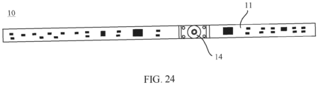
- an electrical element 24 such as a capacitor, a resistor, or an inductor may be further disposed in the circuit board 11. Therefore, in the actual preparation process, after the photosensitive chip 12 is packaged, the electrical element may be further disposed on the circuit board 11 by using a surface-mount technology or the like.
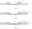
- a camera assembly 10 may further include a light filter 15.
- the light filter 15 may be further disposed on a second mounting surface 132 of the package body 13.
- the package body 13 may alternatively be used to replace the light filter 15.
- the packaging material may cover a light-receiving surface 120 of the photosensitive chip 12.
- a specific component of the packaging material may be properly selected, so that the package body 13 has a light-filtering function.
- a camera lens 14 may be further connected to the package body 13.
- a first mounting surface 131 configured to mount the camera lens 14 may be provided in the package body 13.
- one end of the camera lens 14 may be coated with glue, and then the end coated with the glue is attached to the first mounting surface 131, to implement a fixed connection between the package body 13 and the camera lens 14.
- connection rib may be cut off in a manner of laser cutting, cutting with a cutting tool, or the like, to divide the plurality of circuit boards into independent units.
- the package body 13 may fill the entire region M, when the connection rib is cut, the package body 13 may also be cut at the same time.
- the support board 17 may be further removed, to prevent the support board 17 from increasing a height size of the camera assembly 10.
- the support board 17 may alternatively not be removed, so that structural safety of the circuit board 11 can be ensured.
Landscapes
- Engineering & Computer Science (AREA)
- Theoretical Computer Science (AREA)
- Signal Processing (AREA)
- Computer Hardware Design (AREA)
- Multimedia (AREA)
- Physics & Mathematics (AREA)
- Human Computer Interaction (AREA)
- General Engineering & Computer Science (AREA)
- General Physics & Mathematics (AREA)
- Mathematical Physics (AREA)
- Studio Devices (AREA)
- Camera Bodies And Camera Details Or Accessories (AREA)
- Solid State Image Pick-Up Elements (AREA)
Applications Claiming Priority (2)
| Application Number | Priority Date | Filing Date | Title |
|---|---|---|---|
| CN202210593622.4A CN117201899A (zh) | 2022-05-27 | 2022-05-27 | 一种摄像头组件、摄像头组件的制备方法和电子设备 |
| PCT/CN2023/096183 WO2023227048A1 (zh) | 2022-05-27 | 2023-05-25 | 一种摄像头组件、摄像头组件的制备方法和电子设备 |
Publications (2)
| Publication Number | Publication Date |
|---|---|
| EP4513883A1 true EP4513883A1 (de) | 2025-02-26 |
| EP4513883A4 EP4513883A4 (de) | 2025-07-23 |
Family
ID=88918550
Family Applications (1)
| Application Number | Title | Priority Date | Filing Date |
|---|---|---|---|
| EP23811118.1A Pending EP4513883A4 (de) | 2022-05-27 | 2023-05-25 | Kameraanordnung, herstellungsverfahren für kameraanordnung und elektronische vorrichtung |
Country Status (3)
| Country | Link |
|---|---|
| EP (1) | EP4513883A4 (de) |
| CN (1) | CN117201899A (de) |
| WO (1) | WO2023227048A1 (de) |
Families Citing this family (2)
| Publication number | Priority date | Publication date | Assignee | Title |
|---|---|---|---|---|
| CN117544844B (zh) * | 2024-01-09 | 2025-02-28 | 荣耀终端股份有限公司 | 感光组件、感光芯片的贴装方法、摄像头模组及电子设备 |
| CN119697476B (zh) * | 2025-02-21 | 2025-05-13 | 宁波舜宇光电信息有限公司 | 一种摄像模组 |
Family Cites Families (10)
| Publication number | Priority date | Publication date | Assignee | Title |
|---|---|---|---|---|
| CN101087370B (zh) * | 2006-06-07 | 2010-12-08 | 光宝科技股份有限公司 | 图像感测装置与应用该图像感测装置的镜头模块 |
| US20190148429A1 (en) * | 2016-03-12 | 2019-05-16 | Ningbo Sunny Opotech Co., Ltd. | Camera module, and photosensitive component thereof and manufacturing method therefor |
| WO2018006673A1 (zh) * | 2016-07-03 | 2018-01-11 | 宁波舜宇光电信息有限公司 | 感光组件和摄像模组及其制造方法 |
| CN107404606B (zh) * | 2017-05-06 | 2018-09-14 | 南昌欧菲光电技术有限公司 | 摄像模组 |
| CN112188043A (zh) * | 2019-07-04 | 2021-01-05 | 南昌欧菲生物识别技术有限公司 | 芯片封装结构、摄像头模组和电子设备 |
| CN210491015U (zh) * | 2019-10-28 | 2020-05-08 | Oppo广东移动通信有限公司 | 电子设备、摄像头模组及其电路板组件 |
| CN112995453B (zh) * | 2019-12-18 | 2023-04-18 | 宁波舜宇光电信息有限公司 | 深度信息摄像模组及其组装方法 |
| CN212211129U (zh) * | 2020-04-30 | 2020-12-22 | 华为技术有限公司 | 摄像头模组及电子设备 |
| CN212811821U (zh) * | 2020-08-17 | 2021-03-26 | 南昌欧菲光电技术有限公司 | 摄像头模组、摄像装置及电子设备 |
| CN112702498B (zh) * | 2020-12-29 | 2022-07-01 | 维沃移动通信有限公司 | 摄像头模组及电子设备 |
-
2022
- 2022-05-27 CN CN202210593622.4A patent/CN117201899A/zh active Pending
-
2023
- 2023-05-25 WO PCT/CN2023/096183 patent/WO2023227048A1/zh not_active Ceased
- 2023-05-25 EP EP23811118.1A patent/EP4513883A4/de active Pending
Also Published As
| Publication number | Publication date |
|---|---|
| CN117201899A (zh) | 2023-12-08 |
| EP4513883A4 (de) | 2025-07-23 |
| WO2023227048A1 (zh) | 2023-11-30 |
Similar Documents
| Publication | Publication Date | Title |
|---|---|---|
| EP4513883A1 (de) | Kameraanordnung, herstellungsverfahren für kameraanordnung und elektronische vorrichtung | |
| KR100408614B1 (ko) | 촬상 장치 | |
| KR102321747B1 (ko) | 카메라 모듈과 카메라 모듈을 갖는 전자설비 및 카메라 모듈 제조방법 | |
| EP2814063B1 (de) | Bildgebungseinheit und bildgebungsvorrichtung | |
| EP4216535A1 (de) | Kameramodul und elektronische vorrichtung | |
| WO2021218115A1 (zh) | 摄像头模组及电子设备 | |
| WO2021073182A1 (zh) | 一种摄像模组和电子设备 | |
| EP4048042A1 (de) | Abschirmdeckel, abschirmhaube, leiterplattenanordnung und elektronische vorrichtung | |
| JP2022126814A (ja) | プリント回路板、及び電子機器 | |
| US11895793B2 (en) | Image pickup unit and imaging apparatus | |
| JPH06334298A (ja) | 表面実装部品の搭載構造 | |
| CN116326216A (zh) | 相机模块 | |
| US20230093281A1 (en) | Camera module and electronic device | |
| EP4195642A1 (de) | Elektronische vorrichtung | |
| EP3767936B1 (de) | Fotografiermodul mit abschrägung, lichterfassungsanordnung und elektronische vorrichtung | |
| TWI793799B (zh) | 成像鏡頭模組與電子裝置 | |
| CN116033267B (zh) | 防抖机构、摄像模组及电子设备 | |
| CN222381718U (zh) | 摄像头模组及电子设备 | |
| US20250392661A1 (en) | Electronic device | |
| CN218679216U (zh) | 一种电子设备及摄像头模组 | |
| CN115699781A (zh) | 相机模块和光学装置 | |
| CN216291124U (zh) | 摄像模组和电子设备 | |
| KR102879985B1 (ko) | 카메라 모듈 | |
| CN217283057U (zh) | 摄像感光组件、摄像模组和电子设备 | |
| US20240113141A1 (en) | Electronic component and method of manufacturing the same |
Legal Events
| Date | Code | Title | Description |
|---|---|---|---|
| STAA | Information on the status of an ep patent application or granted ep patent |
Free format text: STATUS: THE INTERNATIONAL PUBLICATION HAS BEEN MADE |
|
| PUAI | Public reference made under article 153(3) epc to a published international application that has entered the european phase |
Free format text: ORIGINAL CODE: 0009012 |
|
| STAA | Information on the status of an ep patent application or granted ep patent |
Free format text: STATUS: REQUEST FOR EXAMINATION WAS MADE |
|
| 17P | Request for examination filed |
Effective date: 20241121 |
|
| AK | Designated contracting states |
Kind code of ref document: A1 Designated state(s): AL AT BE BG CH CY CZ DE DK EE ES FI FR GB GR HR HU IE IS IT LI LT LU LV MC ME MK MT NL NO PL PT RO RS SE SI SK SM TR |
|
| A4 | Supplementary search report drawn up and despatched |
Effective date: 20250620 |
|
| RIC1 | Information provided on ipc code assigned before grant |
Ipc: H04N 23/50 20230101AFI20250613BHEP Ipc: G06F 1/16 20060101ALI20250613BHEP Ipc: H04M 1/02 20060101ALI20250613BHEP Ipc: H04N 23/54 20230101ALI20250613BHEP Ipc: H04N 23/55 20230101ALI20250613BHEP Ipc: H04N 23/57 20230101ALI20250613BHEP Ipc: H10F 39/00 20250101ALI20250613BHEP |
|
| DAV | Request for validation of the european patent (deleted) | ||
| DAX | Request for extension of the european patent (deleted) | ||
| STAA | Information on the status of an ep patent application or granted ep patent |
Free format text: STATUS: EXAMINATION IS IN PROGRESS |