EP4514096A2 - Cellule solaire et son procédé de préparation - Google Patents
Cellule solaire et son procédé de préparation Download PDFInfo
- Publication number
- EP4514096A2 EP4514096A2 EP25151846.0A EP25151846A EP4514096A2 EP 4514096 A2 EP4514096 A2 EP 4514096A2 EP 25151846 A EP25151846 A EP 25151846A EP 4514096 A2 EP4514096 A2 EP 4514096A2
- Authority
- EP
- European Patent Office
- Prior art keywords
- layer
- passivation
- oxide layer
- solar cell
- tunnel oxide
- Prior art date
- Legal status (The legal status is an assumption and is not a legal conclusion. Google has not performed a legal analysis and makes no representation as to the accuracy of the status listed.)
- Pending
Links
Images






Classifications
-
- H—ELECTRICITY
- H10—SEMICONDUCTOR DEVICES; ELECTRIC SOLID-STATE DEVICES NOT OTHERWISE PROVIDED FOR
- H10F—INORGANIC SEMICONDUCTOR DEVICES SENSITIVE TO INFRARED RADIATION, LIGHT, ELECTROMAGNETIC RADIATION OF SHORTER WAVELENGTH OR CORPUSCULAR RADIATION
- H10F77/00—Constructional details of devices covered by this subclass
- H10F77/20—Electrodes
- H10F77/206—Electrodes for devices having potential barriers
- H10F77/211—Electrodes for devices having potential barriers for photovoltaic cells
-
- H—ELECTRICITY
- H10—SEMICONDUCTOR DEVICES; ELECTRIC SOLID-STATE DEVICES NOT OTHERWISE PROVIDED FOR
- H10F—INORGANIC SEMICONDUCTOR DEVICES SENSITIVE TO INFRARED RADIATION, LIGHT, ELECTROMAGNETIC RADIATION OF SHORTER WAVELENGTH OR CORPUSCULAR RADIATION
- H10F77/00—Constructional details of devices covered by this subclass
- H10F77/20—Electrodes
- H10F77/244—Electrodes made of transparent conductive layers, e.g. transparent conductive oxide [TCO] layers
- H10F77/251—Electrodes made of transparent conductive layers, e.g. transparent conductive oxide [TCO] layers comprising zinc oxide [ZnO]
-
- H—ELECTRICITY
- H10—SEMICONDUCTOR DEVICES; ELECTRIC SOLID-STATE DEVICES NOT OTHERWISE PROVIDED FOR
- H10F—INORGANIC SEMICONDUCTOR DEVICES SENSITIVE TO INFRARED RADIATION, LIGHT, ELECTROMAGNETIC RADIATION OF SHORTER WAVELENGTH OR CORPUSCULAR RADIATION
- H10F10/00—Individual photovoltaic cells, e.g. solar cells
- H10F10/10—Individual photovoltaic cells, e.g. solar cells having potential barriers
- H10F10/14—Photovoltaic cells having only PN homojunction potential barriers
-
- H—ELECTRICITY
- H10—SEMICONDUCTOR DEVICES; ELECTRIC SOLID-STATE DEVICES NOT OTHERWISE PROVIDED FOR
- H10F—INORGANIC SEMICONDUCTOR DEVICES SENSITIVE TO INFRARED RADIATION, LIGHT, ELECTROMAGNETIC RADIATION OF SHORTER WAVELENGTH OR CORPUSCULAR RADIATION
- H10F10/00—Individual photovoltaic cells, e.g. solar cells
- H10F10/10—Individual photovoltaic cells, e.g. solar cells having potential barriers
- H10F10/16—Photovoltaic cells having only PN heterojunction potential barriers
- H10F10/164—Photovoltaic cells having only PN heterojunction potential barriers comprising heterojunctions with Group IV materials, e.g. ITO/Si or GaAs/SiGe photovoltaic cells
- H10F10/165—Photovoltaic cells having only PN heterojunction potential barriers comprising heterojunctions with Group IV materials, e.g. ITO/Si or GaAs/SiGe photovoltaic cells the heterojunctions being Group IV-IV heterojunctions, e.g. Si/Ge, SiGe/Si or Si/SiC photovoltaic cells
-
- H—ELECTRICITY
- H10—SEMICONDUCTOR DEVICES; ELECTRIC SOLID-STATE DEVICES NOT OTHERWISE PROVIDED FOR
- H10F—INORGANIC SEMICONDUCTOR DEVICES SENSITIVE TO INFRARED RADIATION, LIGHT, ELECTROMAGNETIC RADIATION OF SHORTER WAVELENGTH OR CORPUSCULAR RADIATION
- H10F71/00—Manufacture or treatment of devices covered by this subclass
- H10F71/121—The active layers comprising only Group IV materials
-
- H—ELECTRICITY
- H10—SEMICONDUCTOR DEVICES; ELECTRIC SOLID-STATE DEVICES NOT OTHERWISE PROVIDED FOR
- H10F—INORGANIC SEMICONDUCTOR DEVICES SENSITIVE TO INFRARED RADIATION, LIGHT, ELECTROMAGNETIC RADIATION OF SHORTER WAVELENGTH OR CORPUSCULAR RADIATION
- H10F71/00—Manufacture or treatment of devices covered by this subclass
- H10F71/129—Passivating
-
- H—ELECTRICITY
- H10—SEMICONDUCTOR DEVICES; ELECTRIC SOLID-STATE DEVICES NOT OTHERWISE PROVIDED FOR
- H10F—INORGANIC SEMICONDUCTOR DEVICES SENSITIVE TO INFRARED RADIATION, LIGHT, ELECTROMAGNETIC RADIATION OF SHORTER WAVELENGTH OR CORPUSCULAR RADIATION
- H10F71/00—Manufacture or treatment of devices covered by this subclass
- H10F71/138—Manufacture of transparent electrodes, e.g. transparent conductive oxides [TCO] or indium tin oxide [ITO] electrodes
-
- H—ELECTRICITY
- H10—SEMICONDUCTOR DEVICES; ELECTRIC SOLID-STATE DEVICES NOT OTHERWISE PROVIDED FOR
- H10F—INORGANIC SEMICONDUCTOR DEVICES SENSITIVE TO INFRARED RADIATION, LIGHT, ELECTROMAGNETIC RADIATION OF SHORTER WAVELENGTH OR CORPUSCULAR RADIATION
- H10F77/00—Constructional details of devices covered by this subclass
- H10F77/20—Electrodes
- H10F77/206—Electrodes for devices having potential barriers
- H10F77/211—Electrodes for devices having potential barriers for photovoltaic cells
- H10F77/215—Geometries of grid contacts
-
- H—ELECTRICITY
- H10—SEMICONDUCTOR DEVICES; ELECTRIC SOLID-STATE DEVICES NOT OTHERWISE PROVIDED FOR
- H10F—INORGANIC SEMICONDUCTOR DEVICES SENSITIVE TO INFRARED RADIATION, LIGHT, ELECTROMAGNETIC RADIATION OF SHORTER WAVELENGTH OR CORPUSCULAR RADIATION
- H10F77/00—Constructional details of devices covered by this subclass
- H10F77/30—Coatings
- H10F77/306—Coatings for devices having potential barriers
- H10F77/311—Coatings for devices having potential barriers for photovoltaic cells
-
- H—ELECTRICITY
- H10—SEMICONDUCTOR DEVICES; ELECTRIC SOLID-STATE DEVICES NOT OTHERWISE PROVIDED FOR
- H10F—INORGANIC SEMICONDUCTOR DEVICES SENSITIVE TO INFRARED RADIATION, LIGHT, ELECTROMAGNETIC RADIATION OF SHORTER WAVELENGTH OR CORPUSCULAR RADIATION
- H10F77/00—Constructional details of devices covered by this subclass
- H10F77/30—Coatings
- H10F77/306—Coatings for devices having potential barriers
- H10F77/311—Coatings for devices having potential barriers for photovoltaic cells
- H10F77/315—Coatings for devices having potential barriers for photovoltaic cells the coatings being antireflective or having enhancing optical properties
-
- H—ELECTRICITY
- H10—SEMICONDUCTOR DEVICES; ELECTRIC SOLID-STATE DEVICES NOT OTHERWISE PROVIDED FOR
- H10F—INORGANIC SEMICONDUCTOR DEVICES SENSITIVE TO INFRARED RADIATION, LIGHT, ELECTROMAGNETIC RADIATION OF SHORTER WAVELENGTH OR CORPUSCULAR RADIATION
- H10F77/00—Constructional details of devices covered by this subclass
- H10F77/70—Surface textures, e.g. pyramid structures
- H10F77/703—Surface textures, e.g. pyramid structures of the semiconductor bodies, e.g. textured active layers
Definitions
- the present application relates to the field of photovoltaic technology, and specifically to solar cells, preparation methods thereof, photovoltaic modules, and photovoltaic systems.
- a tunnel oxide passivated contact (TOPCon) solar cell a tunnel oxide layer and a doped polysilicon layer are typically formed on the surface of a silicon wafer, together constituting a passivated contact structure to provide excellent interface passivation for the silicon wafer.
- the doped polysilicon layer often has significant parasitic light absorption, which reduces photovoltaic conversion efficiency of the solar cell.
- an embodiment of a solar cell includes:
- a material of the transparent conductive oxide layer includes a doped metal oxide.
- the doped metal oxide includes zinc oxide doped with at least one of aluminum, boron, or gallium.
- the doped metal oxide is selected from the group consisting of aluminum-doped zinc oxide, gallium-doped zinc oxide, boron-doped zinc oxide, and any combination thereof.
- a material of the transparent conductive oxide layer includes aluminum-doped zinc oxide, and a mass percentage of aluminum in the aluminum-doped zinc oxide is in a range from 1% to 20%.
- a thickness of the transparent conductive oxide layer is in a range from 5nm to 20nm.
- the passivation medium layer includes a transparent conductive oxide layer and a first passivation layer; the first passivation layer is disposed on a surface of the transparent conductive oxide layer away from the first tunnel oxide layer.
- the passivation medium layer includes at least one transparent conductive oxide layer and at least one first passivation layer.
- the passivation medium layer includes one transparent conductive oxide layer and one first passivation layer, the transparent conductive oxide layer and the first passivation layer are sequentially stacked along a direction away from the first tunnel oxide layer.
- the passivation medium layer includes at least two transparent conductive oxide layers and at least two first passivation layers, the transparent conductive oxide layers and the first passivation layers are alternately stacked along a direction away from the first tunnel oxide layer.
- a material of the first passivation layer is selected from the group consisting of aluminum oxide, silicon nitride, and a combination thereof.
- a thickness of the first passivation layer is in a range from 1nm to 20nm.
- the first surface includes an electrode region and a non-electrode region; orthographic projections of the first tunnel oxide layer and the passivation medium layer on the first surface include an overlapping region; the overlapping region is located at least in the non-electrode region of the first surface.
- the solar cell further includes a first passivating contact layer, and the first passivating contact layer is disposed on the first surface and located in the electrode region.
- the first tunnel oxide layer is in contact with the first surface in the non-electrode region; the first passivating contact layer is disposed on the first surface and located in the electrode region.
- the first tunnel oxide layer includes a first portion and a second portion; the first portion is in contact with the first surface in the non-electrode region; the second portion is spaced from the first surface in the electrode region, the second portion is disposed on a surface of the first passivating contact layer away from the first surface.
- the first passivating contact layer includes a second tunnel oxide layer and a first doped semiconductor layer stacked sequentially on the first surface in the electrode region.
- a thickness of the second tunnel oxide layer is in a range from 0.8nm to 2nm.
- a thickness of the first doped semiconductor layer is in a range from 10nm to 500nm.
- the first tunnel oxide layer comprises a first portion and a second portion; the first portion is in contact with the first surface in the non-electrode region, and the second portion is in contact with the first surface in the electrode region; the first passivating contact layer is disposed on a surface of the second portion away from the substrate.
- the first passivating contact layer includes a first doped semiconductor layer; the first doped semiconductor layer is disposed on a surface of the second portion away from the substrate.
- the first passivating contact layer further includes a second tunnel oxide layer; the second tunnel oxide layer is disposed on a surface of the first doped semiconductor layer away from the second portion.
- the solar cell further includes a first electrode; an orthographic projection of the first electrode on the first surface is located in the electrode region of the first surface, and the first electrode is in Ohmic contact with the first passivating contact layer.
- a size ratio of the first electrode to the first passivating contact layer is greater than 0 and less than or equal to 1.
- the solar cell further includes a second passivation layer; the second passivation layer is disposed on a surface of the passivation medium layer away from the first tunnel oxide layer.
- the solar cell further includes a second passivating contact layer; the second passivating contact layer is disposed on the second surface of the substrate.
- the second passivating contact layer includes a third tunnel oxide layer and a second doped semiconductor layer sequentially stacked on the second surface.
- a thickness of the third tunnel oxide layer is in a range from 0.8nm to 2nm.
- a thickness of the second doped semiconductor layer is in a range from 10nm to 1000nm.
- the solar cell further includes a third passivation layer; the third passivation layer is disposed on a surface of the second passivating contact layer away from the substrate.
- a thickness of the first tunnel oxide layer is in a range from 0.8nm to 2nm.
- an embodiment of a method for preparing a solar cell includes:
- a material of the transparent conductive oxide layer includes a doped metal oxide.
- the doped metal oxide is selected from the group consisting of aluminum-doped zinc oxide, gallium-doped zinc oxide, boron-doped zinc oxide, and any combination thereof.
- a material of the transparent conductive oxide layer includes aluminum-doped zinc oxide, and a mass percentage of aluminum in the aluminum-doped zinc oxide is in a range from 1% to 20%.
- forming the passivation medium layer includes forming a transparent conductive oxide layer and a first passivation layer; the first passivation layer is formed on a surface of the transparent conductive oxide layer away from the first tunnel oxide layer.
- forming the passivation medium layer includes forming at least one transparent conductive oxide layer and at least one first passivation layer.
- forming the passivation medium layer includes forming one transparent conductive oxide layer and forming one first passivation layer, the transparent conductive oxide layer and the first passivation layer are sequentially formed and stacked along a direction away from the first tunnel oxide layer.
- forming the passivation medium layer includes forming at least two transparent conductive oxide layers and forming at least two first passivation layers, the transparent conductive oxide layers and the first passivation layers are alternately formed and stacked along a direction away from the first tunnel oxide layer.
- a material of the first passivation layer is selected from the group consisting of aluminum oxide, silicon nitride, and a combination thereof.
- the first surface includes an electrode region and a non-electrode region; before sequentially forming the first tunnel oxide layer and the passivation medium layer on the first surface of the substrate, the method further includes:
- the first tunnel oxide layer includes a first portion and a second portion; the first portion is in contact with the first surface in the non-electrode region; the second portion is spaced from the first surface in the electrode region, and the second portion is formed on a surface of the first passivating contact layer away from the first surface.
- forming the first passivating contact layer includes forming a second tunnel oxide layer and a first doped semiconductor layer, which are stacked sequentially on the first surface in the electrode region.
- the method further includes: forming a first electrode on the first surface of the substrate, wherein an orthographic projection of the first electrode on the first surface is located in the electrode region of the first surface, and the first electrode is in Ohmic contact with the first passivating contact layer.
- the method further includes: forming a second passivation layer on a surface of the passivation medium layer away from the first tunnel oxide layer.
- the method further includes forming a second passivating contact layer on the second surface of the substrate.
- the method further includes forming a second electrode on the second surface of the substrate, wherein the second electrode is in Ohmic contact with the second passivating contact layer.
- the method further includes forming a third passivation layer on a surface of the second passivating contact layer away from the substrate.
- an embodiment of a photovoltaic module includes the solar cell in any one of the above embodiments.
- an embodiment of a photovoltaic system includes the solar module in any one of the above embodiments.
- the first tunnel oxide layer and the passivation medium layer are sequentially stacked on the first surface of the substrate to form a staked structure, the first tunnel oxide layer is at least partially in contact with the first surface, and the passivation medium layer includes at least the transparent conductive oxide layer.
- the passivation medium layer includes at least the transparent conductive oxide layer.
- first and second are used merely as labels to distinguish one element having a certain name from another element having the same name, and cannot be understood as indicating or implying any priority, precedence, or order of one element over another, or indicating the quantity of the element. Therefore, the element modified by “first” or “second” may explicitly or implicitly includes at least one of the elements. In the description of the present application, "a plurality of” means at least two, such as two, three, etc., unless otherwise specifically defined.
- the terms “installed”, “connected”, “coupled”, “fixed” and the like should be interpreted broadly.
- an element, when being referred to as being “installed”, “connected”, “coupled”, “fixed” to another element, unless otherwise specifically defined may be fixedly connected, detachably connected, or integrated to the other element, may be mechanically connected or electrically connected to the other element, and may be directly connected to the other element or connected to the other element via an intermediate element.
- an element when being referred to as being disposed “on” or “under” another element, e.g., a surface, may be in direct contact with the other element or contact the other element via an intermediate element.
- the element when being referred to as being disposed “on”, “above”, “over” another element, may be located right above or obliquely above the other element, or merely located at a horizontal level higher than the other element; the element, when being referred to as being disposed “under”, “below”, “beneath” another element, may be located right below or obliquely below the other element, or merely located at a horizontal level lower than the other element.
- an element when being referred to as being “fixed” or “mounted” to another element, may be directly fixed or mounted to the other element or via an intermediate element.
- Such terms as “vertical”, “horizontal”, “up”, “down”, “left”, “right” and the like used herein are for illustrative purposes only and are not meant to be the only ways for implementing the present application.
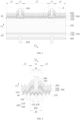
- FIG. 1 is a schematic structural view of a solar cell in an embodiment of the present application.
- FIG. 2 is a partial enlarged view of area A in FIG. 1 . For clarity, only the features relevant to the embodiments of the present application are shown.
- an embodiment of the present application provides a solar cell, including a substrate 100, a first tunnel oxide layer 200, and a passivation medium layer 300.
- the substrate 100 is configured to receive incident light and generate photogenerated carriers.
- the solar cell can be a tunnel oxide passivated contact (TOPCon) solar cell.
- the material of the substrate 100 can be selected according to actual needs.
- the substrate 100 can be a silicon wafer.
- the doping type of the substrate 100 is not limited.
- the substrate 100 can be an n-type doped silicon wafer or a p-type doped silicon wafer, which is not specifically limited in the embodiments of the present application.
- the substrate 100 can be an n-type monocrystalline silicon wafer.
- the substrate 100 includes a first surface m1 and a second surface m2 opposite to the first surface m1.
- the first surface m1 and the second surface m2 are two opposite surfaces.
- the first surface m1 and the second surface m2 are opposite to each other along a first direction F1.
- the first direction F1 is the thickness direction of the substrate 100.
- Both the first surface m1 and the second surface m2 can be used to receive incident light.
- the first surface m1 is the light-receiving surface
- the second surface m2 is the back surface.
- the light-receiving surface and the back surface are relative terms, and in a solar cell or a photovoltaic module, the light-receiving surface specifically refers to the surface of the substrate 100 which most of sunlight irradiates. With the development of the solar cell technology, the back surface also can receive the sunlight, mainly from the reflected light or scattered light in the surrounding environment, and make use of light energy.
- the first surface m1 commonly includes a textured structure for increasing the light absorption area, thereby enhancing the photocurrent and improving the conversion efficiency of the solar cell.
- the first tunnel oxide layer 200 is adapted to provide an interface passivation for the first surface m1 of the substrate 100, achieving chemical passivation. Specifically, by saturating the dangling bonds on the surface of the substrate 100 and reducing the interface defect state density of the first surface m1 of the substrate 100, the recombination centers at the first surface m1 of the substrate 100 can be reduced, and thus the recombination rate of carriers can be reduced.
- the material of the first tunnel oxide layer 200 can be a dielectric material, such as at least one of silicon oxide, magnesium fluoride, amorphous silicon, polysilicon, silicon carbide, silicon nitride, silicon oxynitride, aluminum oxide, or titanium oxide. In a specific embodiment, the first tunnel oxide layer 200 is made of silicon oxide. Other tunnel oxide layers mentioned below can have similar functions and/or be made of similar materials as the first tunnel oxide layer 200, which will not be repeatedly described herein.
- the first tunnel oxide layer 200 is disposed on the first surface m1 of the substrate 100.
- the first tunnel oxide layer 200 is at least partially in contact with the first surface m1 of the substrate 100. That is, a portion or the entirety of the first tunnel oxide layer 200 is in contact with the first surface m1 of the substrate 100, or a portion or the entirety of the first surface m1 of the substrate 100 is in contact with the first tunnel oxide layer 200.
- the entirety of the first tunnel oxide layer 200 can be in contact with the first surface m1, while the first tunnel oxide layer 200 can cover the entirety of the first surface m1 or cover only a portion of the first surface m1.
- the first tunnel oxide layer 200 can include a portion in contact with the first surface m1 and another portion not in contact with the first surface m1.
- the passivation medium layer 300 is disposed on a surface of the first tunnel oxide layer 200 away from the substrate 100.
- the passivation medium layer 300 mainly functions to provide surface passivation in the solar cell, effectively chemically passivating the dangling bonds on the surface of the substrate 100.
- the passivation medium layer 300 can have a single-layer or multi-layer structure.
- the passivation medium layer 300 includes at least a transparent conductive oxide layer 310.
- the transparent conductive oxide layer 310 is a layer structure made of transparent conductive oxide material, with high light transmittance and low electrical resistivity. That is, when the passivation medium layer 300 is a single-layer structure, the passivation medium layer 300 is the transparent conductive oxide layer 310.
- the passivation medium layer 300 includes multiple transparent conductive oxide layers 310, or includes at least one transparent conductive oxide layer 310 and at least one other layer.
- the transparent conductive oxide layer 310 is disposed on the surface of the first tunnel oxide layer 200 away from the substrate 100, and the other layers in the multi-layer structure are stacked on the surface of the transparent conductive oxide layer 310 away from the first tunnel oxide layer 200.
- the other layers in the multi-layer structure can include another transparent conductive oxide layer 310, a passivation layer, etc.
- the passivation medium layer 300 is a single-layer structure, i.e., is the transparent conductive oxide layer 310.
- a tunnel oxide layer and a doped polysilicon layer, together forming a passivating contact structure, are both formed on the first surface m1
- the notable light absorption ability of the doped polysilicon layer will lead to significant parasitic light absorption and current loss.
- the doped polysilicon layer is further heavily doped to increase the degree of band bending at the surface of the substrate 100, the light absorption ability of the heavily doped polysilicon layer will be further enhanced, and the parasitic light absorption of the doped polysilicon layer will be more severe, making it even more difficult to solve the problem of current loss.
- the passivating contact structure is formed by the passivation medium layer 300 and the first tunnel oxide layer 200, and the passivation medium layer 300 includes at least the transparent conductive oxide layer 310. Since the transparent conductive oxide layer 310 has high light transmittance, the light absorption ability of the transparent conductive oxide layer 310 is much lower than that of a doped polysilicon layer. Moreover, a more significant band bending can be formed at the first surface m1 of the substrate 100. Thus, not only the parasitic light absorption caused by unwanted light absorption can be reduced, but also field passivation for minority carriers and selective transmission for majority carriers can be achieved. Consequently, a better surface passivation effect can be achieved, and the carrier recombination current density can be reduced.
- the first tunnel oxide layer 200 and the passivation medium layer 300 together form a stacked structure, in which the passivation medium layer 300 includes at least the transparent conductive oxide layer 310.
- the passivation medium layer 300 includes at least the transparent conductive oxide layer 310.
- the material of the transparent conductive oxide layer 310 includes a doped metal oxide.
- the doped metal oxide is zinc oxide doped with at least one of aluminum, boron, or gallium.
- the doped metal oxide is any one or a combination of aluminum-doped zinc oxide, gallium-doped zinc oxide, or boron-doped zinc oxide.
- the material of the transparent conductive oxide layer 310 can be selected according to actual needs.
- the material of the transparent conductive oxide layer 310 includes aluminum-doped zinc oxide. Since aluminum-doped zinc oxide can cause a more significant band bending at the first surface m1 of the substrate 100, the carrier recombination current density can be further reduced.
- a mass percentage of aluminum in the aluminum-doped zinc oxide is in a range from 1% to 20%.
- the mass percentage of aluminum in the aluminum-doped zinc oxide can be 1%, 2%, 3%, 5%, 6%, 8%, 9.5%, 10%, 11%, 13%, 15%, 17%, 19%, or 20%.
- the transparent conductive oxide layer 310 with the range of mass percentage of aluminum can have an adequate electrical conductivity.
- a thickness of the transparent conductive oxide layer 310 is in a range from 5 nm to 20 nm.
- the thickness of the transparent conductive oxide layer can be 5 nm, 6 nm, 7 nm, 8 nm, 9 nm, 10 nm, 12 nm, 14 nm, 15 nm, 17 nm, 18 nm, 19 nm, or 20 nm.
- the transparent conductive oxide layer 310 within the range of thickness can have excellent electrical and optical performances.
- the range of thickness can reduce both the sheet resistance and the production cost of the transparent conductive oxide layer 310.
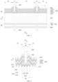
- FIG. 3 is a schematic structural view of a solar cell in another embodiment of the present application.
- FIG. 4 is a partial enlarged view of area B in FIG. 3 .
- FIG. 5 is a schematic structural view of a solar cell in yet another embodiment of the present application.
- FIG. 6 is a partial enlarged view of area C in FIG. 5 .
- FIG. 3 is a schematic structural view of a solar cell in another embodiment of the present application.
- FIG. 4 is a partial enlarged view of area B in FIG. 3 .
- FIG. 5 is a schematic structural view of a solar cell in yet another embodiment of the present application.
- FIG. 6 is a partial enlarged view of area C in FIG. 5 .
- FIG. 5 For clarity, only the features relevant to the embodiments of the present application are shown.
- the passivation medium layer 300 further includes a first passivation layer 320.
- the first passivation layer 320 mainly functions to provide surface passivation in the solar cell and can have a single-layer or multi-layer structure.
- the passivation medium layer 300 includes a transparent conductive oxide layer 310 and a first passivation layer 320.
- the transparent conductive oxide layer 310 is disposed on a surface of the first tunnel oxide layer 200 away from the substrate 100, and the first passivation layer 320 is disposed on a surface of the transparent conductive oxide layer 310 away from the first tunnel oxide layer 200.
- the passivation medium layer 300 includes at least one transparent conductive oxide layer 310 and at least one first passivation layer 320.
- the solar cell includes a single transparent conductive oxide layer 310 and a single first passivation layer 320
- the transparent conductive oxide layer 310 and the first passivation layer 320 are sequentially stacked along a direction, e.g., the first direction F1, away from the first tunnel oxide layer 200.
- the solar cell includes two or more transparent conductive oxide layers 310 and two or more first passivation layers 320
- the transparent conductive oxide layers 310 and the first passivation layers 320 are alternately stacked along the direction away from the first tunnel oxide layer 200.
- alternate stacking refers to the arrangement that one first passivation layer 320 is sandwiched between two adjacent transparent conductive oxide layers 310.
- a stacked structure can be formed by sequentially stacking a transparent conductive oxide layer 310, a first passivation layer 320, a transparent conductive oxide layer 310, a first passivation layer 320, a transparent conductive oxide layer 310..., and a last first passivation layer 320.
- the farthest layer from the first tunnel oxide layer 200 can be either a transparent conductive oxide layer 310 or a first passivation layer 320.
- the solar cell includes two transparent conductive oxide layers 310 and a single first passivation layer 320.
- the two transparent conductive oxide layers 310 include a first transparent conductive oxide layer 310a and a second transparent conductive oxide layer 310b.
- the first transparent conductive oxide layer 310a, the first passivation layer 320, and the second transparent conductive oxide layer 310b are sequentially stacked on the surface of the first tunnel oxide layer 200 away from the substrate 100.
- the first passivation layer(s) 320 disposed between the transparent conductive oxide layers 310 in the passivation medium layer 300 can further improve the passivation effect on the first surface m1 of the substrate 100.
- the material of the first passivation layer 320 includes aluminum oxide, silicon nitride, or a combination thereof.
- the material of the first passivation layer 320 can be selected according to actual needs.
- the material of the transparent conductive oxide layer 310 can be aluminum-doped zinc oxide
- the material of the first passivation layer 320 can be aluminum oxide.
- Aluminum oxide can suppress hydrogen release, which ensures sufficient hydrogen passivation at the transparent conductive oxide layer 310 and the first tunnel oxide layer 200, therefore the synergistic effect between the transparent conductive oxide layer 310, which provides the field passivation, and the first passivation layer 320, which provides the hydrogen passivation, can further enhance the passivation effect, thereby significantly improving the conversion efficiency of the solar cell.
- the thickness of the first passivation layer 320 is in a range from 1nm to 20nm.
- the thickness of the first passivation layer 320 can be 1nm, 2nm, 3nm, 5nm, 6nm, 7nm, 8nm, 9nm, 10nm, 12nm, 14nm, 15nm, 17nm, 18nm, 19nm, or 20nm.
- the first passivation layer 320 within the range of thickness can provide adequate passivation effect and possess adequate carrier transporting capability.
- the first surface m1 of the substrate 100 includes an electrode region z1 and a non-electrode region z2.
- the electrode region z1 is a region where any electrode is formed.
- the non-electrode region z2 is the region without any electrode, i.e., the region of the first surface m1 excluding the electrode region z1.
- Orthographic projections of the first tunnel oxide layer 200 and the passivation medium layer 300 on the first surface m1 include an overlapping region, and the overlapping region is located at least in the non-electrode region z2 of the first surface m1.
- the passivation medium layer 300 covers the surface of the first tunnel layer 200 away from the substrate 100, and the overlapping projection can be located at least in the non-electrode region z2 of the first surface m1, therefore the first tunnel oxide layer 200 and the passivation medium layer 300 are located in correspondence with at least the non-electrode region z2 of the first surface m1.
- the overlapping projection can be located in both the non-electrode region z2 and the electrode region z1 of the first surface m1, and thus the first tunnel oxide layer 200 and the passivation medium layer 300 are located in correspondence with both the non-electrode region z2 and the electrode region z1 of the first surface m1.
- FIGs. 1 to 6 show some embodiments in which the first tunnel oxide layer 200 and the passivation medium layer 300 are located in correspondence with both the non-electrode region z2 and the electrode region z1 of the first surface m1.
- the carrier recombination in the non-electrode region z2 of the first surface m1 can be reduced, thereby improving the conversion efficiency of the solar cell.
- the carrier recombination in both the electrode region z1 and the non-electrode region z2 of the first surface m1 can be further reduced, thereby further improving the conversion efficiency of the solar cell.
- the solar cell further includes a first passivating contact layer 400, which is disposed on the first surface m1 and located in the electrode region z1.
- the electrode region z1 and the non-electrode region z2 of the first surface m1 are defined by being with or without the first passivating contact layer 400.
- the region of the first surface m1 covered with the first passivating contact layer 400 is the electrode region z1
- the region of the first surface m1 not covered with the first passivating contact layer 400 is the non-electrode region z2.
- the electrode formed on the first surface m1 can be in Ohmic contact with the first passivating contact layer 400.
- the carrier recombination at the electrode region z1 of the first surface m1 can be reduced, while the contact between the electrode and the electrode region z1 of the first surface m1 can be improved, thereby greatly improving the conversion efficiency of the solar cell.
- the first tunnel oxide layer 200 is in contact with the non-electrode region z2 of the first surface m1.
- the first passivating contact layer 400 is disposed on the first surface m1 and located in the electrode region z1, e.g., in contact with the electrode region z1 of the first surface m1.
- the electrode formed in the electrode region z1 can be in Ohmic contact with and thereby electrically connected to the first passivating contact layer 400, thereby improving the contact performance.
- the first tunnel oxide layer 200 can be formed after removing the first passivating contact layer 400 in the non-electrode region z2, damage to the first tunnel oxide layer 200 can be reduced.
- the first tunnel oxide layer 200 includes a first portion 210 located in the non-electrode region z2 and in contact with the first surface m1, and a second portion 220 located in the electrode region z1 and spaced from the first surface m1.
- the second portion 220 is disposed on a surface of the first passivating contact layer 400 away from the first surface m1.
- the passivation medium layer 300 can also include two portions, which are a third portion disposed on a surface of the first portion 210 away from the substrate 100 and a fourth portion disposed on a surface of the second portion 220 away from the substrate 100. That is, the passivation medium layer 300 covers the entire surface of the first tunnel oxide layer 200 away from the substrate 100.
- the part of the electrode region z1 of the first surface m1 that is not covered with the electrode can be covered with the first tunnel oxide layer 200 and the passivation medium layer 300, so that the carrier recombination in the electrode region z1 can be further reduced and the efficiency of the solar cell can be enhanced.
- the first tunnel oxide layer 200 is only located in the non-electrode region z2 of the first surface m1, and the first tunnel oxide layer 200 is in contact with the non-electrode region z2 of the first surface m1.
- the first tunnel oxide layer 200 only includes the first portion 210.
- the solar cell can include the first passivating contact layer 400, and the first passivating contact layer 400 is disposed on the first surface m1 and located in the electrode region z1. However, the surface of the first passivating contact layer 400 away from the first surface m1 is not covered with the first tunnel oxide layer 200.
- the first passivating contact layer 400 away from the first surface m1 is entirely covered with the electrode.
- the passivation medium layer 300 is only located in the non-electrode region z2 of the first surface m1, only including the third portion.
- the first passivating contact layer 400 includes a second tunnel oxide layer 410 and a first doped semiconductor layer 420, which are sequentially stacked on the first surface in the electrode region.
- the first doped semiconductor layer 420 can be an n-type doped semiconductor layer or a p-type doped semiconductor layer.
- the n-type doped semiconductor layer can be an n-type amorphous silicon layer, an n-type microcrystalline silicon layer, an n-type polysilicon layer, or an n-type nanocrystalline silicon layer, which can be selected according to actual needs and is not limited herein.
- the first doped semiconductor layer 420 is an n-type doped polysilicon layer.
- the second tunnel oxide layer 410 is adapted to provide surface passivation, and the first doped semiconductor layer 420 can act as a carrier-selective contact material. As such, the second tunnel oxide layer 410 and the first doped semiconductor layer 420 together form a passivating contact structure on the first surface m1 in the electrode region z1, thereby reducing carrier recombination and providing good contact performance, and thus improving the efficiency of the solar cell and facilitating the formation of the electrode in the electrode region z1 on the first surface m1.
- a thickness of the second tunnel oxide layer 410 is in a range from 0.8nm to 2nm.
- the thickness of the second tunnel oxide layer 410 can be 0.8nm, 0.9nm, 1nm, 1.1nm, 1.3nm, 1.4nm, 1.6nm, 1.9nm, or 2nm.
- the second tunnel oxide layer 410 within the range of thickness can provide an adequate passivation effect and have a reduced contact resistance, thereby preventing the decrease in the fill factor of the solar cell caused by the contact resistance.
- a thickness of the first doped semiconductor layer 420 is in a range from 10nm to 500nm.
- the thickness of the first doped semiconductor layer 420 can be 10nm, 20nm, 30nm, 50nm, 70nm, 80nm, 90nm, 100nm, 110nm, 120nm, 170nm, 190nm, 200nm, 210nm, 220nm, 270nm, 290nm, 300nm, 310nm, 320nm, 370nm, 390nm, 400nm, 410nm, 420nm, 470nm, 490nm, or 500nm.
- the first doped semiconductor layer 420 within the range of thickness can selectively transport charge carriers, reducing recombination loss, and also can reduce optical absorption path, reducing parasitic light absorption, thereby improving the conversion efficiency of the solar cell.
- the passivating contact structure including the first tunnel oxide layer 200 and the first passivation layer 320 located at least in the non-electrode region z2 of the first surface m1 can reduce carrier recombination.
- the first doped semiconductor layer 420 is located only in the electrode region z1 of the first surface m1, and thus the area of the first doped semiconductor layer 420 can be reduced, which reduces parasitic light absorption of the first doped semiconductor layer 420 while facilitating the fabrication of the electrode on the electrode region z1 of the first surface m1.
- FIG. 9 is a schematic structural view of a solar cell in yet another embodiment of the present application.
- FIG. 10 is a partial enlarged view of area D in FIG. 9 .
- FIG. 11 is a partial enlarged view of a solar cell in yet another embodiment of the present application. For clarity, only the features relevant to the embodiments of the present application are shown.
- the first tunnel oxide layer 200 includes a first portion 210 located on and in contact with the non-electrode region z2 of the first surface m1, and a second portion 220 located on and in contact with the electrode region z1 of the first surface m1. That is, the first tunnel oxide layer 200 covers the first surface m1, and the entirety of the first tunnel oxide layer 200 can be in contact with the first surface m1.
- the first passivating contact layer 400 is located in the electrode region z1 and disposed on a surface of the second portion 220 away from the substrate 100. That is, the first passivating contact layer 400 is spaced from the first surface m1 of the substrate 100 by the second portion 220 of the first tunnel oxide layer 200.
- the first passivating contact layer 400 includes a first doped semiconductor layer 420, which is disposed on the surface of the second portion 220 away from the substrate 100.
- the first doped semiconductor layer 420 and the second portion 220 of the first tunnel oxide layer 200 can form a passivating contact structure.
- the first passivating contact layer 400 includes a first doped semiconductor layer 420 and a second tunnel oxide layer 410.
- the second tunnel oxide layer 410 is disposed on a surface of the first doped semiconductor layer 420 away from the second portion 220.
- the first doped semiconductor layer 420 and the second tunnel oxide layer 410 are sequentially stacked on the surface of the second portion 220 away from the substrate 100.
- the first doped semiconductor layer 420 and the second tunnel oxide layer 410 form a passivating contact structure, and the first passivating contact layer 400 and the first tunnel oxide layer 200 also can be seen as forming another passivating contact structure.
- the other features of the second tunnel oxide layer 410 and the first doped semiconductor layer 420 can be referred to those described in the above embodiments, and are not repeated herein.
- the passivating contact structure can be flexibly formed through the first passivating contact layer 400 and the first tunnel oxide layer 200 as described in the above embodiments.
- a passivating contact structure is formed to include the first doped semiconductor layer 420 disposed between the second portion 220 of the first tunnel layer and the second tunnel oxide layer 410.
- the embodiments in FIGs. 2 , 4 , and 6 are easier to be fabricated.
- the solar cell further includes a first electrode 500.
- An orthographic projection of the first electrode 500 on the first surface m1 is located in the electrode region z1 of the first surface m1.
- the first electrode 500 is in Ohmic contact with the first passivating contact layer 400.
- the first electrode 500 is formed corresponding to the electrode region z1 of the first surface m1, and the first electrode 500 can be in contact with but not penetrating through the first doped semiconductor layer 420, thereby maintaining a good interface passivation.
- the first electrode 500 can penetrate sequentially through the passivation medium layer 300 and the first tunnel oxide layer 200, and come into contact with the first doped semiconductor layer 420.
- the first electrode 500 can be in contact with the first doped semiconductor layer 420.
- the first tunnel oxide layer 200 in the embodiments where the first tunnel oxide layer 200 is also in contact with the electrode region z1 of the first surface m1, the first tunnel oxide layer 200 can penetrate through the passivation medium layer 300 and come into contact with the first doped semiconductor layer 420, or the first tunnel oxide layer 200 can sequentially penetrate through the passivation medium layer 300 and the second tunnel oxide layer 410, and come into contact with the first doped semiconductor layer 420.
- the first electrode 500 can be made of a metal material, including one or more conductive metals, such as Ag, Ni, Cu, Sn, Al, etc., which can be selected according to actual needs and is not limited herein.
- a metal material including one or more conductive metals, such as Ag, Ni, Cu, Sn, Al, etc., which can be selected according to actual needs and is not limited herein.
- a second direction F2 can be the width direction of the first electrode 500 and perpendicular to the first direction F1.
- a size ratio of the first electrode 500 to the first passivating contact layer 400 is greater than 0 and less than or equal to 1.
- the size of the first electrode 500 along the second direction F2 is a first size d1
- the size of the first passivating contact layer 400 along the second direction F2 is a second size d2
- the ratio of the first size d1 to the second size d2 is greater than 0 and less than or equal to 1, e.g., can be 0.1, 0.2, 0.3, 0.4, 0.5, 0.6, 0.7, 0.8, 0.9, or 1.
- the first size d1 is smaller than the second size d2. In the embodiments in FIGs. 7 and 8 , the first size d1 is equal to the second size d2. In the embodiments in FIGs. 7 and 8 , the first tunnel oxide layer 200 is located in the non-electrode region z2 of the first surface m1 and is in contact with the non-electrode region z2 of the first surface m1.
- the size of the electrode region z1 of the first surface m1 can be represented by the second size d2.
- the size of the second tunnel oxide layer 410 and the size of the first doped semiconductor layer 420 along the second direction F2 can both be the second size d2.
- the ratio of the first size d1 to the second size d2 within the above range facilitates the fabrication of the first electrode 500 and improves the conversion efficiency of the solar cell.
- the solar cell further includes a second passivation layer 600.
- the second passivation layer 600 is disposed on a surface of the passivation medium layer 300 away from the first tunnel oxide layer 200.
- the second passivation layer 600 is disposed on a surface of the transparent conductive oxide layer 310 away from the first tunnel oxide layer 200.
- the second passivation layer 600 is disposed on a surface of the first passivation layer 320 away from the transparent conductive oxide layer 310.
- the second passivation layer 600 is disposed on a surface of the second transparent conductive oxide layer 310b away from the first passivation layer 320.
- the first electrode 500 can penetrate through the second passivation layer 600, the passivation medium layer 300, and the first tunnel oxide layer 200, and come into contact with the first doped semiconductor layer 420.
- the second passivation layer 600 mainly functions as surface passivation and anti-reflection in the solar cell.
- the second passivation layer 600 can chemically passivate the dangling bonds on the surface of the substrate 100 and have an anti-reflection effect.
- the second passivation layer 600 can be a single-layer structure or a multi-layer structure.
- the material of the second passivation layer 600 can be at least one of aluminum oxide, silicon oxide, silicon nitride, or silicon oxynitride. In a specific embodiment, the material of the second passivation layer 600 is silicon nitride.
- the solar cell further includes a second passivating contact layer 700.
- the second passivating contact layer 700 is disposed on the second surface m2 of the substrate 100.
- the electrode formed on the second surface m2 can be in Ohmic contact with and thus electrically connected to the second passivation contact layer 700.
- the carrier recombination at the second surface m2 can be reduced, while the contact between the electrode and the second surface m2 can be improved, thereby greatly improving the conversion efficiency of the solar cell.
- the second passivation contact layer 700 includes a third tunnel oxide layer 710 and a second doped semiconductor layer 720 stacked in sequence on the second surface m2 of the substrate 100.
- the second doped semiconductor layer 720 can be an n-type doped semiconductor layer or a p-type doped semiconductor layer.
- the p-type doped semiconductor layer can be a p-type amorphous silicon layer, a p-type microcrystalline silicon layer, a p-type polysilicon layer, or a p-type nanocrystalline silicon layer, which can be selected according to actual needs and is not limited herein.
- the second doped semiconductor layer 720 is a p-type doped semiconductor layer.
- the third tunnel oxide layer 710 is adapted to provide surface passivation, and the second doped semiconductor layer 720 can act as a carrier-selective contact material. As such, the third tunnel oxide layer 710 and the second doped semiconductor layer 720 together form a passivating contact structure on the second surface m2, thereby reducing carrier recombination and providing good contact performance, thus improving the efficiency of the solar cell and facilitating the formation of the electrode on the second surface m2.
- a thickness of the third tunnel oxide layer 710 is in a range from 0.8 nm to 2 nm.
- the thickness of the third tunnel oxide layer 710 can be 0.8 nm, 0.9 nm, 1 nm, 1.1 nm, 1.3 nm, 1.4 nm, 1.6 nm, 1.9 nm, or 2 nm.
- the third tunnel oxide layer 710 within the range of thickness can provide an adequate passivation effect and have a reduced contact resistance, thereby preventing the decrease in the fill factor of the solar cell caused by the contact resistance.
- a thickness of the second doped semiconductor layer 720 is in a range of 10 nm to 1000 nm.
- the thickness of the second doped semiconductor layer 720 can be 10 nm, 20 nm, 30 nm, 50 nm, 70 nm, 80 nm, 90 nm, 100 nm, 110 nm, 120 nm, 170 nm, 190 nm, 200 nm, 210 nm, 220 nm, 270 nm, 290 nm, 300 nm, 310 nm, 320 nm, 370 nm, 390 nm, 400 nm, 410 nm, 420 nm, 470 nm, 490 nm, 500 nm, 510 nm, 520 nm, 570 nm, 590 nm, 600 nm, 610 n
- the second doped semiconductor layer 720 within the range of thickness can selectively transport charge carriers, reducing recombination loss, and also can reduce optical absorption path, reducing parasitic light absorption, thereby improving the conversion efficiency of the solar cell.
- the solar cell further includes a second electrode 800.
- the second electrode 800 is disposed on the second surface m2 of the substrate 100, and is in Ohmic contact with the second passivation contact layer 700. Specifically, the second electrode 800 can be in contact with but not penetrating through the second doped semiconductor layer 720, thereby maintaining good interface passivation.
- the second electrode 800 can be made of a metal material, including one or more conductive metals, such as Ag, Ni, Cu, Sn, Al, etc., which can be selected according to actual needs and is not limited herein.
- a metal material including one or more conductive metals, such as Ag, Ni, Cu, Sn, Al, etc., which can be selected according to actual needs and is not limited herein.
- the solar cell further includes a third passivation layer 900.
- the third passivation layer 900 is disposed on a surface of the second passivating contact layer 700 away from the substrate 100.
- the third passivation layer 900 is disposed on a surface of the second doped semiconductor layer 720 away from the third tunnel oxide layer 710.
- the second electrode 800 can penetrate through the third passivation layer 900 and come into contact with the second doped semiconductor layer 720.
- the third passivation layer 900 mainly functions as surface passivation and anti-reflection in the solar cell.
- the third passivation layer 900 can chemically passivate the dangling bonds on the surface of the substrate 100 and have an anti-reflection effect.
- the third passivation layer 900 can be a single-layer structure or a multi-layer structure.
- the material of the third passivation layer 900 can be at least one of aluminum oxide, silicon oxide, silicon nitride, or silicon oxynitride. In a specific embodiment, the material of the third passivation layer 900 is silicon nitride.
- a thickness of the first tunnel oxide layer 200 is in a range from 0.8 nm to 2 nm.
- the thickness of the first tunnel oxide layer 200 can be 0.8 nm, 0.9 nm, 1 nm, 1.1 nm, 1.3 nm, 1.4 nm, 1.6 nm, 1.9 nm, or 2 nm.
- the first tunnel oxide layer 200 within the range of thickness can provide an adequate passivation effect and have a reduced contact resistance, thereby preventing the decrease in the fill factor of the solar cell caused by the contact resistance.
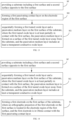
- FIG. 12 shows a flow chart of a method for preparing a solar cell in an embodiment of the present application. For clarity, only relevant features are shown.
- an embodiment of the present application provides a method for preparing a solar cell, and the method includes steps of:
- a silicon wafer as the substrate 100 can be cleaned, textured, and at least one surface of the silicon wafer in the thickness direction can be polished to form the second surface m2 of the substrate 100.
- a textured structure is formed in the first surface m1 of the substrate 100.
- the texturing is optional and can be performed or not according to actual needs, and is not limited herein.
- the first tunnel oxide layer 200 can be formed by using a method involving thermal oxidation, plasma oxidation, and/or nitric acid oxidation; the transparent conductive oxide layer 310 can be formed by using a method involving atomic layer deposition and/or physical vapor deposition.
- the structures and materials of the substrate 100, the first tunnel oxide layer 200, the passivation medium layer 300, and the transparent conductive oxide layer 310 have been described above and are not repeated herein.
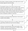
- FIG. 13 shows a flow chart of a method for preparing a solar cell including step SH in an embodiment of the present application. For clarity, only relevant features are shown.
- the first surface m1 of the substrate 100 includes an electrode region z1 and a non-electrode region z2.
- the first tunnel oxide layer 200 is in contact with the non-electrode region z2 of the first surface m1.
- the method further includes: SH, forming a first passivating contact layer 400 on the first surface m1 in the electrode region z1.
- the first passivating contact layer 400 can be firstly formed on the first surface m1 of the substrate 100, and then the portion of the first passivating contact layer 400 located in the non-electrode region z2 of the first surface m1 can be removed using laser etching or chemical etching, leaving the other portion of the first passivating contact layer 400 located in the electrode region z1 of the first surface m1.
- the structures as shown in FIGs. 2 , 4 , and 6 to 8 can be formed by the methods including such a step.
- the first tunnel oxide layer 200 is formed after the removal step, such as the laser or chemical etching step, thus avoiding the damage to the first tunnel oxide layer 200 in the removal step, and improving the passivation performance of the first tunnel oxide layer 200.
- the removal step such as the laser or chemical etching step
- the size of the electrode region z1 along the second direction F2 is greater than the size of the electrode along the second direction F2 (i.e., the width of the electrode) on the first surface m1
- the process window for forming the electrode can be increased.
- the first passivating contact layer 400 includes the first doped semiconductor layer 420, as the first doped semiconductor layer 420 has relatively good thermal endurance, the contact performance of the electrode can be improved.
- the first doped semiconductor layer 420 can be formed by using low-pressure chemical vapor deposition (LPCVD), plasma-enhanced chemical vapor deposition (PECVD), or physical vapor deposition (PVD).
- LPCVD low-pressure chemical vapor deposition
- PECVD plasma-enhanced chemical vapor deposition
- PVD physical vapor deposition
- the first tunnel oxide layer 200 can be firstly formed on the first surface m1 of the substrate 100, and then the first passivating contact layer 400 can be formed on the electrode region z1 of the first surface m1.
- the structures as shown in FIGs. 10 and 11 can be formed by the methods including such a step.
- the features of the first passivating contact layer 400 can be referred to those described in the above embodiments, and are not repeated herein.
- the sidewall of the first doped semiconductor layer 420 is in contact with the first tunnel oxide layer 200.
- the first doped semiconductor layer 420 is covered by the first tunnel oxide layer 200.
- the first electrode 500 penetrates through the second portion 220 of the first tunnel oxide layer 200 and then comes into Ohmic contact with the first doped semiconductor layer 420.
- the sidewall of the first doped semiconductor layer 420 is in contact with the transparent conductive oxide layer 310.
- the first doped semiconductor layer 420 is disposed on the first tunnel oxide layer 200, and the exposed surface of the first doped semiconductor layer 420 is covered by the transparent conductive oxide layer 310.
- the first electrode 500 penetrates through the transparent conductive oxide layer 310 and then comes into Ohmic contact with the first doped semiconductor layer 420.
- first passivating contact layer 400 and the structure formed by the first passivating contact layer 400 and the first tunnel oxide layer 200 can be referred to those described in the above relevant embodiments of the solar cell, and are not repeated herein.
- FIG. 14 shows a flow chart of a method for preparing a solar cell including step SI in an embodiment of the present application. For clarity, only relevant features are shown.
- the method includes: SI, forming the first electrode 500 on the first surface m1 of the substrate 100, where an orthographic projection of the first electrode 500 on the first surface m1 is located in the electrode region z1 of the first surface m1, and the first electrode 500 is in Ohmic contact with the first passivating contact layer 400.
- the first electrode 500 can be formed by the method such as screen printing, electroplating, or laser transfer printing, and is not specifically limited herein.
- the features of the first electrode 500 can be referred to those described in the above relevant embodiments of the solar cell, and are not repeated herein.
- FIG. 15 shows a flow chart of a method for preparing a solar cell including step SJ in an embodiment of the present application. For clarity, only relevant features are shown.
- the method includes: SJ, forming a second passivation layer 600 on a surface of the passivation medium layer 300 away from the first tunnel oxide layer 200.
- Step SJ can be performed before step SI to facilitate the forming process.
- the first electrode 500 can firstly penetrate through the second passivation layer 600, and then penetrate through at least the passivation medium layer 300, and finally come into Ohmic contact with the first doped semiconductor layer 420.
- the features of the second passivation layer 600 can be referred to those described in the above embodiments, and are not repeated herein.
- FIG. 16 shows a flow chart of a method for preparing a solar cell including step SK in an embodiment of the present application. For clarity, only relevant features are shown.
- the method further includes: SK, forming a second passivating contact layer 700 on the second surface m2 of the substrate 100.
- the features of the second passivating contact layer 700 can be referred to those described in the above embodiments, and are not repeated herein.
- step SK can be performed before step SG or after step SG.
- the step of forming the third tunnel oxide layer 710 can be performed simultaneously with or separately from the step of forming the first tunnel oxide layer 200 or the step of forming the second tunnel oxide layer 410, which can be decided according to actual structural needs and is not limited herein.
- the second passivating contact layer 700 includes a third tunnel oxide layer 710 and a second doped semiconductor layer, these layers can be formed according to the processes for forming similar layers in the above embodiments.
- FIG. 17 shows a flow chart of a method for preparing a solar cell including step SL in an embodiment of the present application. For clarity, only relevant features are shown.
- the method includes: SL, forming a second electrode 800 on the second surface m2 of the substrate 100, where the second electrode 800 is in Ohmic contact with the second passivating contact layer 700.
- the features of the second electrode 800 can be referred to those described in the above embodiments, and are not repeated herein.
- FIG. 18 shows a flow chart of a method for preparing a solar cell including step SM in an embodiment of the present application. For clarity, only relevant features are shown.
- the method further includes: SM, forming a third passivation layer 900 on a surface of the second passivating contact layer 700 away from the substrate 100.
- the features of the third passivation layer 900 can be referred to those described in the above embodiments, and are not repeated herein.
- a method for preparing a solar cell includes following steps:
- a method for preparing a solar cell includes following steps:
- steps or stages described above are not necessarily be completed simultaneously but can be performed at different times.
- the steps or stages are not strictly performed in sequence, but can be performed alternately or in turn with at least some of the other steps or sub-steps or stages in the other steps, which can be selected according to actual needs and are not limited herein.
- the solar cells in the embodiments of the present application are exemplarily described below on the basis of some examples and comparative examples.
- Example 1 the structure of the solar cell as shown in FIGs. 3 and 4 is employed.
- the substrate 110 of the solar cell is an n-type silicon wafer with a thickness of 120 ⁇ m.
- the first surface m1 of the substrate 110 serves as the light-receiving surface, while the second surface m2 serves as the back surface.
- the first tunnel oxide layer 200, the second tunnel oxide layer 410, and the third tunnel oxide layer 710 are all made of silicon dioxide, each with a thickness of 1.4nm.
- the transparent conductive oxide layer 310 is made of aluminum-doped zinc oxide with a thickness of 10cm, and the mass percentage of aluminum in the aluminum-doped zinc oxide is 12%.
- the first doped semiconductor layer 420 is an n-type doped polysilicon layer with a thickness of 150nm.
- the second doped semiconductor layer 720 is a p-type doped polysilicon layer with a thickness of 200nm.
- the first passivation layer 320 is made of aluminum oxide, with a thickness ranging from 3nm to 100nm.
- the second passivation layer 600 and the third passivation layer 900 are both made of silicon nitride.
- the thickness of the second passivation layer 600 is 70nm, and the thickness of the third passivation layer 900 is 80nm.
- the first electrode 500 and the second electrode 800 are both made of silver.
- the first electrode 500 located on the first surface m1 includes 18 busbar electrode lines and 200 finger electrode lines, where the width of each busbar electrode line is 200 ⁇ m, and the width of each finger electrode line is 20 ⁇ m.
- the size of the electrode region z1 of the first surface m1 along the second direction F2 is 100 ⁇ m.
- the second electrode 800 located on the second surface m2 includes 18 busbar electrode lines and 200 finger electrode lines, where the width of each busbar electrode line is 200 ⁇ m, and the width of each finger electrode line is 20 ⁇ m.
- Example 2 is different from Example 1 in that in Example 2 the transparent conductive oxide layer 310 is made of aluminum-doped zinc oxide and has a thickness of 5nm, and the mass percentage of aluminum in the aluminum-doped zinc oxide is 1%.
- Example 3 is different from Example 1 in that in Example 3 the transparent conductive oxide layer 310 is made of aluminum-doped zinc oxide and has a thickness of 5nm, and the mass percentage of aluminum in the aluminum-doped zinc oxide is 20%.
- Example 4 is different from Example 1 in that in Example 4 the transparent conductive oxide layer 310 is made of aluminum-doped zinc oxide and has a thickness of 20nm, and the mass percentage of aluminum in the aluminum-doped zinc oxide is 1%.
- Example 5 is different from Example 1 in that in Example 5 the transparent conductive oxide layer 310 is made of aluminum-doped zinc oxide and has a thickness of 20nm, and the mass percentage of aluminum in the aluminum-doped zinc oxide is 20%.
- Example 6 is different from Example 1 in that in Example 6 the transparent conductive oxide layer 310 is made of aluminum-doped zinc oxide and has a thickness of 5nm, and the mass percentage of aluminum in the aluminum-doped zinc oxide is 15%.
- Example 7 is different from Example 1 in that in Example 7 the transparent conductive oxide layer 310 is made of gallium-doped zinc oxide and has a thickness of 10nm, and the mass percentage of gallium in the gallium-doped zinc oxide is 12%.
- Example 8 is different from Example 1 in that in Example 8 the transparent conductive oxide layer 310 is made of gallium-doped zinc oxide and has a thickness of 5nm, and the mass percentage of gallium in the gallium-doped zinc oxide is 1%.
- Example 9 is different from Example 1 in that in Example 9 the transparent conductive oxide layer 310 is made of boron-doped zinc oxide and has a thickness of 5nm, and the mass percentage of boron in the boron-doped zinc oxide is 20%.
- Example 10 is different from Example 1 in that in Example 10 the transparent conductive oxide layer 310 is made of boron-doped zinc oxide and has a thickness of 20nm, and the mass percentage of boron in the boron-doped zinc oxide is 15%.
- Example 11 is different from Example 1 in that the structure of the solar cell as shown in FIGs. 1 and 2 is employed, and the solar cell in Example 11 does not include the first passivation layer 320.
- Example 12 is different from Example 2 in that the structure of the solar cell as shown in FIGs. 1 and 2 is employed, and the solar cell in Example 12 does not include the first passivation layer 320.
- Example 13 is different from Example 3 in that the structure of the solar cell as shown in FIGs. 1 and 2 is employed, and the solar cell in Example 13 does not include the first passivation layer 320.
- Example 14 is different from Example 4 in that the structure of the solar cell as shown in FIGs. 1 and 2 is employed, and the solar cell in Example 14 does not include the first passivation layer 320.
- Example 15 is different from Example 5 in that the structure of the solar cell as shown in FIGs. 1 and 2 is employed, and the solar cell in Example 15 does not include the first passivation layer 320.
- Example 16 is different from Example 6 in that the structure of the solar cell as shown in FIGs. 1 and 2 is employed, and the solar cell in Example 16 does not include the first passivation layer 320.
- Example 17 is different from Example 7 in that the structure of the solar cell as shown in FIGs. 1 and 2 is employed, and the solar cell in Example 17 does not include the first passivation layer 320.
- Example 18 is different from Example 8 in that the structure of the solar cell as shown in FIGs. 1 and 2 is employed, and the solar cell in Example 18 does not include the first passivation layer 320.
- Example 19 is different from Example 9 in that the structure of the solar cell as shown in FIGs. 1 and 2 is employed, and the solar cell in Example 19 does not include the first passivation layer 320.
- Example 20 is different from Example 10 in that the structure of the solar cell as shown in FIGs. 1 and 2 is employed, and the solar cell in Example 20 does not include the first passivation layer 320.
- Example 21 is different from Example 1 in that the transparent conductive oxide layer 310 is made of aluminum-doped zinc oxide and has a thickness of 4nm, and the mass percentage of aluminum in the aluminum-doped zinc oxide is 0.5%.
- Example 22 is different from Example 21 in that the structure of the solar cell as shown in FIGs. 1 and 2 is employed, and the solar cell in Example 22 does not include the first passivation layer 320.
- Example 23 is different from Example 1 in that the transparent conductive oxide layer 310 is made of aluminum-doped zinc oxide and has a thickness of 22nm, and the mass percentage of aluminum in the aluminum-doped zinc oxide is 22%.
- Example 24 is different from Example 23 in that the structure of the solar cell as shown in FIGs. 1 and 2 is employed, and the solar cell in Example 24 does not include the first passivation layer 320.
- Example 25 is different from Example 1 in that the transparent conductive oxide layer 310 is made of aluminum-doped zinc oxide and has a thickness of 4nm, and the mass percentage of aluminum in the aluminum-doped zinc oxide is 30%.
- Example 26 is different from Example 25 in that the structure of the solar cell as shown in FIGs. 1 and 2 is employed, and the solar cell in Example 26 does not include the first passivation layer 320.
- Example 27 is different from Example 1 in that the transparent conductive oxide layer 310 is made of aluminum-doped zinc oxide and has a thickness of 22nm, and the mass percentage of aluminum in the aluminum-doped zinc oxide is 0.2%.
- Example 28 is different from Example 27 in that the structure of the solar cell as shown in FIGs. 1 and 2 is employed, and the solar cell in Example 28 does not include the first passivation layer 320.
- Example 29 is different from Example 1 in that the transparent conductive oxide layer 310 is made of gallium-doped zinc oxide and has a thickness of 22nm, and the mass percentage of gallium in the gallium-doped zinc oxide is 0.2%.
- Example 30 is different from Example 29 in that the structure of the solar cell as shown in FIGs. 1 and 2 is employed, and the solar cell in Example 30 does not include the first passivation layer 320.
- Example 31 is different from Example 1 in that the transparent conductive oxide layer 310 is made of boron-doped zinc oxide and has a thickness of 30nm, and the mass percentage of boron in the boron-doped zinc oxide is 30%.
- Example 32 is different from Example 31 in that the structure of the solar cell as shown in FIGs. 1 and 2 is employed, the solar cell in Example 32 does not include the first passivation layer 320.
- the structure on the second surface m2 of the substrate 100 is the same as that in Example 1.
- the structure on the first surface m1 of the substrate 100 is the same as that on the second surface m2 of the substrate 100. That is, the structure on the first surface m1 of the substrate 100 sequentially includes a tunnel oxide layer 710', a doped polysilicon layer 720', a passivation layer 900', and an electrode 500.
- the structure on the first surface m1 of the substrate 100 is completely identical to the structure on the second surface m2 of the substrate 100 in all features such as location, shape, size, and material.
- Comparative Example 2 is different from Comparative Example 1 only in the non-electrode region z2 of the first surface m1 of the substrate 100.
- the electrode region z1 on the first surface m1 of the substrate 100 there are sequentially the tunnel oxide layer 710', the doped polysilicon layer 720', the passivation layer 900', and the electrode 500, with materials and thicknesses consistent with those in Comparative Example 1.
- the portions of the tunnel oxide layer 710' and the doped polysilicon layer 720' in the non-electrode region z2 on the first surface m1 of the substrate 100 are replaced with a phosphorus-doped layer 730'.
- the solar cells from Examples 1 to 32 and Comparative Examples 1 to 2 are subjected to electrical performance tests using a transient simulator device under the conditions of a light source of simulated sunlight of 100mW/cm 2 , AM1.5G, and a temperature of 25 degrees Celsius.
- the test results are shown in Table 1.
- the solar cells in Examples 1 to 32 exhibit higher conversion efficiencies and greater fill factors. Specifically, compared with Comparative Example 1, Examples 1 to 32 exhibit greater open-circuit voltages and short-circuit currents. Compared with Comparative Example 2, Examples 1 to 32 exhibit greater open-circuit voltages and fill factors.
- the transparent conductive oxide layer is made of aluminum-doped zinc oxide, and has higher photovoltaic conversion efficiency than the transparent conductive oxide layers made of other metal oxides. Of course, the photovoltaic conversion efficiency of other examples is also improved compared with Comparative Example 1 and Comparative Example 2.
- an embodiment of the present application provides a photovoltaic module, including one or more solar cells described in any one of the above embodiments, or including one or more solar cells prepared by the method described in any one of the above embodiments.
- the photovoltaic module includes multiple solar cells.
- the solar cells can be electrically connected to form a whole piece or multiple pieces, such as forming a plurality of cell groups.
- the plurality of cell groups are electrically connected in series and/or in parallel.
- the photovoltaic device can further include an encapsulation layer and a cover plate.
- the encapsulation layer is configured to cover the surface of the cell groups, and the cover plate is configured to cover the surface of the encapsulation layer away from the cell groups.
- multiple cell groups can be electrically connected through conductive busbars.
- the encapsulation layer covers the surface of the solar cell.
- the encapsulation layer can be an organic encapsulation film such as an ethylene-vinyl acetate copolymer film, a polyethylene-octene elastomer film, or a polyethylene terephthalate film.
- the cover plate can be a cover plate with a light-transmitting function, such as a glass cover plate or a plastic cover plate.
- an embodiment of the present application provides a photovoltaic system, including one or more photovoltaic modules described in any one of the above embodiments.
- the effects of the photovoltaic module in any one of the embodiments described above are also possessed by the photovoltaic system, and are not repeated herein.
- the photovoltaic system can be applied to photovoltaic power stations, such as ground power stations, roof power stations, water surface power stations, etc., and can also be applied to equipment or devices that use solar energy to generate electricity, such as user solar power supplies, solar street lights, solar cars, solar buildings, etc. It also can be understood that the application scenarios of the photovoltaic system are not limited to the above, that is to say, the photovoltaic system can be applied in all fields in which solar energy is needed to generate electricity.
- the photovoltaic system can include photovoltaic arrays, a combiner box, and an inverter.
- the photovoltaic array can be an array of photovoltaic modules.
- multiple photovoltaic modules can form multiple photovoltaic arrays.
- the photovoltaic arrays are connected to the combiner box.
- the combiner box can combine the currents generated by the photovoltaic arrays.
- the combined current flows through the inverter and is converted into the alternating current suitable for the power grid, and then conducted to the power grid to realize solar power supply.
Landscapes
- Photovoltaic Devices (AREA)
- Formation Of Insulating Films (AREA)
Applications Claiming Priority (1)
| Application Number | Priority Date | Filing Date | Title |
|---|---|---|---|
| CN202410373895.7A CN117995919B (zh) | 2024-03-29 | 2024-03-29 | 太阳能电池及其制作方法、光伏组件及光伏系统 |
Publications (2)
| Publication Number | Publication Date |
|---|---|
| EP4514096A2 true EP4514096A2 (fr) | 2025-02-26 |
| EP4514096A3 EP4514096A3 (fr) | 2025-07-16 |
Family
ID=90894395
Family Applications (2)
| Application Number | Title | Priority Date | Filing Date |
|---|---|---|---|
| EP24189352.8A Pending EP4425572A3 (fr) | 2024-03-29 | 2024-07-18 | Cellule solaire et son procédé de préparation |
| EP25151846.0A Pending EP4514096A3 (fr) | 2024-03-29 | 2025-01-14 | Cellule solaire et son procédé de préparation |
Family Applications Before (1)
| Application Number | Title | Priority Date | Filing Date |
|---|---|---|---|
| EP24189352.8A Pending EP4425572A3 (fr) | 2024-03-29 | 2024-07-18 | Cellule solaire et son procédé de préparation |
Country Status (6)
| Country | Link |
|---|---|
| US (2) | US12575218B2 (fr) |
| EP (2) | EP4425572A3 (fr) |
| JP (2) | JP2024150542A (fr) |
| CN (2) | CN120730886A (fr) |
| AU (2) | AU2024227401A1 (fr) |
| MX (1) | MX2025003108A (fr) |
Families Citing this family (2)
| Publication number | Priority date | Publication date | Assignee | Title |
|---|---|---|---|---|
| CN120730886A (zh) * | 2024-03-29 | 2025-09-30 | 天合光能股份有限公司 | 太阳能电池及其制作方法、光伏组件及光伏系统 |
| CN119866067B (zh) * | 2025-03-24 | 2025-06-13 | 金阳(泉州)新能源科技有限公司 | 抗光致衰减的背接触电池及其制作方法和光伏组件 |
Family Cites Families (25)
| Publication number | Priority date | Publication date | Assignee | Title |
|---|---|---|---|---|
| US9972740B2 (en) * | 2015-06-07 | 2018-05-15 | Tesla, Inc. | Chemical vapor deposition tool and process for fabrication of photovoltaic structures |
| PT3321973T (pt) * | 2016-11-09 | 2021-03-16 | Meyer Burger Germany Ag | Célula solar cristalina com uma camada transparente e condutora entre os contactos de lado dianteiro e procedimento para fabrico de uma tal célula solar |
| CN107195699B (zh) * | 2017-07-12 | 2023-04-14 | 泰州中来光电科技有限公司 | 一种钝化接触太阳能电池及制备方法 |
| CN112201701B (zh) * | 2020-09-30 | 2024-05-03 | 浙江晶科能源有限公司 | 太阳能电池和光伏组件 |
| TWM606270U (zh) * | 2020-10-08 | 2021-01-01 | 聯合再生能源股份有限公司 | 穿隧氧化層鈍化接觸太陽能電池 |
| CN112466962B (zh) * | 2020-11-19 | 2021-11-23 | 晶科绿能(上海)管理有限公司 | 太阳能电池 |
| CN214336723U (zh) | 2020-12-04 | 2021-10-01 | 一道新能源科技(衢州)有限公司 | 一种太阳能电池 |
| CN113506832A (zh) * | 2021-08-05 | 2021-10-15 | 天合光能股份有限公司 | 钝化接触结构、其制备方法以及其应用的太阳能电池 |
| CN215731736U (zh) * | 2021-08-05 | 2022-02-01 | 天合光能股份有限公司 | 钝化接触结构以及其应用的太阳能电池 |
| CN217306521U (zh) * | 2021-12-03 | 2022-08-26 | 晶科能源股份有限公司 | 一种太阳能电池及一种光伏组件 |
| CN114005888A (zh) | 2021-12-30 | 2022-02-01 | 杭州晶宝新能源科技有限公司 | 一种太阳能电池及其制备方法 |
| CN115274927A (zh) * | 2022-08-02 | 2022-11-01 | 青海黄河上游水电开发有限责任公司西宁太阳能电力分公司 | 一种TOPCon太阳能电池的制作方法 |
| CN117712199A (zh) * | 2022-09-08 | 2024-03-15 | 浙江晶科能源有限公司 | 太阳能电池及光伏组件 |
| CN118156325A (zh) * | 2022-12-07 | 2024-06-07 | 浙江晶科能源有限公司 | 太阳能电池及光伏组件 |
| CN116759484A (zh) | 2023-05-23 | 2023-09-15 | 天合光能股份有限公司 | 太阳能电池及其制作方法 |
| CN219677267U (zh) * | 2023-05-29 | 2023-09-12 | 天合光能股份有限公司 | 一种太阳能电池结构 |
| CN116913985A (zh) | 2023-06-26 | 2023-10-20 | 滁州捷泰新能源科技有限公司 | 一种正面采用Ag浆电极的TOPCon电池及其制备方法 |
| CN116914012A (zh) * | 2023-07-19 | 2023-10-20 | 滁州捷泰新能源科技有限公司 | 一种双面掺杂多晶硅钝化接触电池及其制备方法 |
| CN117059679A (zh) * | 2023-08-16 | 2023-11-14 | 中环新能(安徽)先进电池制造有限公司 | 一种太阳能电池的钝化接触复合层及其制备方法和应用 |
| CN117199193A (zh) | 2023-10-12 | 2023-12-08 | 天合光能股份有限公司 | 太阳电池及其制备方法 |
| CN117438480A (zh) | 2023-10-30 | 2024-01-23 | 天合光能股份有限公司 | 透明导电接触钝化的异质结太阳电池及电池组件 |
| CN117457777A (zh) * | 2023-11-07 | 2024-01-26 | 深圳市捷佳伟创新能源装备股份有限公司 | 一种太阳能电池及其制备方法与应用 |
| CN117558831B (zh) * | 2023-11-23 | 2025-09-12 | 四川逸仙光伏产业创新中心有限公司 | 一种硅基异质结太阳能电池的透明导电钝化接触结构及其制备方法 |
| CN117423763A (zh) | 2023-12-19 | 2024-01-19 | 天合光能股份有限公司 | 太阳能电池及其制备方法和太阳能电池组件 |
| CN120730886A (zh) | 2024-03-29 | 2025-09-30 | 天合光能股份有限公司 | 太阳能电池及其制作方法、光伏组件及光伏系统 |
-
2024
- 2024-03-29 CN CN202410893549.1A patent/CN120730886A/zh active Pending
- 2024-03-29 CN CN202410373895.7A patent/CN117995919B/zh active Active
- 2024-07-16 JP JP2024113152A patent/JP2024150542A/ja not_active Withdrawn
- 2024-07-18 EP EP24189352.8A patent/EP4425572A3/fr active Pending
- 2024-08-16 US US18/806,855 patent/US12575218B2/en active Active
- 2024-10-17 AU AU2024227401A patent/AU2024227401A1/en not_active Withdrawn
-
2025
- 2025-01-03 US US19/009,203 patent/US20250151453A1/en active Pending
- 2025-01-10 JP JP2025004165A patent/JP2025061207A/ja active Pending
- 2025-01-14 EP EP25151846.0A patent/EP4514096A3/fr active Pending
- 2025-01-23 AU AU2025200457A patent/AU2025200457B2/en active Active
- 2025-03-14 MX MX2025003108A patent/MX2025003108A/es unknown
Also Published As
| Publication number | Publication date |
|---|---|
| CN117995919B (zh) | 2024-08-16 |
| AU2025200457A1 (en) | 2025-02-13 |
| CN117995919A (zh) | 2024-05-07 |
| JP2025061207A (ja) | 2025-04-10 |
| CN120730886A (zh) | 2025-09-30 |
| AU2025200457B2 (en) | 2026-03-26 |
| AU2024227401A1 (en) | 2024-11-07 |
| EP4425572A3 (fr) | 2025-02-19 |
| EP4425572A2 (fr) | 2024-09-04 |
| US12575218B2 (en) | 2026-03-10 |
| MX2025003108A (es) | 2025-04-02 |
| US20250151453A1 (en) | 2025-05-08 |
| JP2024150542A (ja) | 2024-10-23 |
| EP4514096A3 (fr) | 2025-07-16 |
| US20250311476A1 (en) | 2025-10-02 |
Similar Documents
| Publication | Publication Date | Title |
|---|---|---|
| CN118099245B (zh) | 背接触太阳能电池及其制备方法、光伏组件 | |
| JP7564974B2 (ja) | 太陽光電池及び太陽光発電モジュール | |
| CN109728103B (zh) | 太阳能电池 | |
| CN204928739U (zh) | 双面太阳能面板和双面太阳能电池 | |
| EP4514096A2 (fr) | Cellule solaire et son procédé de préparation | |
| US12464850B2 (en) | Solar cell, method for manufacturing the same, photovoltaic module and photovoltaic system | |
| JP7618868B1 (ja) | 太陽電池及びその製造方法、光起電力モジュール | |
| EP1995792A2 (fr) | Cellule solaire et son procédé de fabrication | |
| US12166142B1 (en) | Solar cell, method for preparing the same, and photovoltaic module | |
| US20100243042A1 (en) | High-efficiency photovoltaic cells | |
| EP2816609B1 (fr) | Cellule solaire | |
| CN105118874A (zh) | 一种晶体硅太阳能电池及其制作方法 | |
| JP2026065666A (ja) | 太陽電池、太陽電池の製造方法及び光起電力モジュール | |
| JP6143520B2 (ja) | 結晶シリコン系太陽電池およびその製造方法 | |
| CN223714520U (zh) | 太阳能电池、光伏组件及光伏系统 | |
| CN223626271U (zh) | 高效n型背接触太阳能电池、光伏组件及光伏系统 | |
| CN223626266U (zh) | 背接触电池 | |
| CN214753783U (zh) | 一种太阳能电池叠层钝化结构 | |
| CN120676712A (zh) | 背接触太阳能电池及其制备方法 | |
| CN119317245A (zh) | 太阳能电池及其制备方法、光伏组件 | |
| CN121310717A (zh) | 背接触太阳能电池及其制备方法、叠层电池及光伏组件 | |
| CN119545970A (zh) | 太阳能电池结构及其制备方法、光伏组件 | |
| CN120603374A (zh) | 太阳能电池及其制备方法和光伏组件 |
Legal Events
| Date | Code | Title | Description |
|---|---|---|---|
| PUAI | Public reference made under article 153(3) epc to a published international application that has entered the european phase |
Free format text: ORIGINAL CODE: 0009012 |
|
| STAA | Information on the status of an ep patent application or granted ep patent |
Free format text: STATUS: REQUEST FOR EXAMINATION WAS MADE |
|
| 17P | Request for examination filed |
Effective date: 20250114 |
|
| AK | Designated contracting states |
Kind code of ref document: A2 Designated state(s): AL AT BE BG CH CY CZ DE DK EE ES FI FR GB GR HR HU IE IS IT LI LT LU LV MC ME MK MT NL NO PL PT RO RS SE SI SK SM TR |
|
| PUAL | Search report despatched |
Free format text: ORIGINAL CODE: 0009013 |
|
| AK | Designated contracting states |
Kind code of ref document: A3 Designated state(s): AL AT BE BG CH CY CZ DE DK EE ES FI FR GB GR HR HU IE IS IT LI LT LU LV MC ME MK MT NL NO PL PT RO RS SE SI SK SM TR |
|
| RIC1 | Information provided on ipc code assigned before grant |
Ipc: H10F 77/30 20250101AFI20250611BHEP Ipc: H10F 77/20 20250101ALI20250611BHEP Ipc: H10F 10/165 20250101ALI20250611BHEP |