EP4514103A1 - Anzeigetafel und anzeigevorrichtung - Google Patents
Anzeigetafel und anzeigevorrichtung Download PDFInfo
- Publication number
- EP4514103A1 EP4514103A1 EP23902400.3A EP23902400A EP4514103A1 EP 4514103 A1 EP4514103 A1 EP 4514103A1 EP 23902400 A EP23902400 A EP 23902400A EP 4514103 A1 EP4514103 A1 EP 4514103A1
- Authority
- EP
- European Patent Office
- Prior art keywords
- layer
- transistor
- gate
- pixel circuit
- signal line
- Prior art date
- Legal status (The legal status is an assumption and is not a legal conclusion. Google has not performed a legal analysis and makes no representation as to the accuracy of the status listed.)
- Pending
Links
Images

















Classifications
-
- H—ELECTRICITY
- H10—SEMICONDUCTOR DEVICES; ELECTRIC SOLID-STATE DEVICES NOT OTHERWISE PROVIDED FOR
- H10K—ORGANIC ELECTRIC SOLID-STATE DEVICES
- H10K59/00—Integrated devices, or assemblies of multiple devices, comprising at least one organic light-emitting element covered by group H10K50/00
- H10K59/10—OLED displays
- H10K59/12—Active-matrix OLED [AMOLED] displays
- H10K59/121—Active-matrix OLED [AMOLED] displays characterised by the geometry or disposition of pixel elements
- H10K59/1213—Active-matrix OLED [AMOLED] displays characterised by the geometry or disposition of pixel elements the pixel elements being TFTs
-
- H—ELECTRICITY
- H10—SEMICONDUCTOR DEVICES; ELECTRIC SOLID-STATE DEVICES NOT OTHERWISE PROVIDED FOR
- H10K—ORGANIC ELECTRIC SOLID-STATE DEVICES
- H10K59/00—Integrated devices, or assemblies of multiple devices, comprising at least one organic light-emitting element covered by group H10K50/00
- H10K59/10—OLED displays
- H10K59/12—Active-matrix OLED [AMOLED] displays
- H10K59/121—Active-matrix OLED [AMOLED] displays characterised by the geometry or disposition of pixel elements
-
- H—ELECTRICITY
- H10—SEMICONDUCTOR DEVICES; ELECTRIC SOLID-STATE DEVICES NOT OTHERWISE PROVIDED FOR
- H10D—INORGANIC ELECTRIC SEMICONDUCTOR DEVICES
- H10D86/00—Integrated devices formed in or on insulating or conducting substrates, e.g. formed in silicon-on-insulator [SOI] substrates or on stainless steel or glass substrates
- H10D86/40—Integrated devices formed in or on insulating or conducting substrates, e.g. formed in silicon-on-insulator [SOI] substrates or on stainless steel or glass substrates characterised by multiple TFTs
- H10D86/421—Integrated devices formed in or on insulating or conducting substrates, e.g. formed in silicon-on-insulator [SOI] substrates or on stainless steel or glass substrates characterised by multiple TFTs having a particular composition, shape or crystalline structure of the active layer
- H10D86/423—Integrated devices formed in or on insulating or conducting substrates, e.g. formed in silicon-on-insulator [SOI] substrates or on stainless steel or glass substrates characterised by multiple TFTs having a particular composition, shape or crystalline structure of the active layer comprising semiconductor materials not belonging to the Group IV, e.g. InGaZnO
-
- H—ELECTRICITY
- H10—SEMICONDUCTOR DEVICES; ELECTRIC SOLID-STATE DEVICES NOT OTHERWISE PROVIDED FOR
- H10D—INORGANIC ELECTRIC SEMICONDUCTOR DEVICES
- H10D86/00—Integrated devices formed in or on insulating or conducting substrates, e.g. formed in silicon-on-insulator [SOI] substrates or on stainless steel or glass substrates
- H10D86/40—Integrated devices formed in or on insulating or conducting substrates, e.g. formed in silicon-on-insulator [SOI] substrates or on stainless steel or glass substrates characterised by multiple TFTs
- H10D86/441—Interconnections, e.g. scanning lines
-
- H—ELECTRICITY
- H10—SEMICONDUCTOR DEVICES; ELECTRIC SOLID-STATE DEVICES NOT OTHERWISE PROVIDED FOR
- H10D—INORGANIC ELECTRIC SEMICONDUCTOR DEVICES
- H10D86/00—Integrated devices formed in or on insulating or conducting substrates, e.g. formed in silicon-on-insulator [SOI] substrates or on stainless steel or glass substrates
- H10D86/40—Integrated devices formed in or on insulating or conducting substrates, e.g. formed in silicon-on-insulator [SOI] substrates or on stainless steel or glass substrates characterised by multiple TFTs
- H10D86/60—Integrated devices formed in or on insulating or conducting substrates, e.g. formed in silicon-on-insulator [SOI] substrates or on stainless steel or glass substrates characterised by multiple TFTs wherein the TFTs are in active matrices
-
- H—ELECTRICITY
- H10—SEMICONDUCTOR DEVICES; ELECTRIC SOLID-STATE DEVICES NOT OTHERWISE PROVIDED FOR
- H10K—ORGANIC ELECTRIC SOLID-STATE DEVICES
- H10K59/00—Integrated devices, or assemblies of multiple devices, comprising at least one organic light-emitting element covered by group H10K50/00
- H10K59/10—OLED displays
- H10K59/12—Active-matrix OLED [AMOLED] displays
- H10K59/121—Active-matrix OLED [AMOLED] displays characterised by the geometry or disposition of pixel elements
- H10K59/1216—Active-matrix OLED [AMOLED] displays characterised by the geometry or disposition of pixel elements the pixel elements being capacitors
-
- H—ELECTRICITY
- H10—SEMICONDUCTOR DEVICES; ELECTRIC SOLID-STATE DEVICES NOT OTHERWISE PROVIDED FOR
- H10K—ORGANIC ELECTRIC SOLID-STATE DEVICES
- H10K59/00—Integrated devices, or assemblies of multiple devices, comprising at least one organic light-emitting element covered by group H10K50/00
- H10K59/10—OLED displays
- H10K59/12—Active-matrix OLED [AMOLED] displays
- H10K59/13—Active-matrix OLED [AMOLED] displays comprising photosensors that control luminance
-
- H—ELECTRICITY
- H10—SEMICONDUCTOR DEVICES; ELECTRIC SOLID-STATE DEVICES NOT OTHERWISE PROVIDED FOR
- H10K—ORGANIC ELECTRIC SOLID-STATE DEVICES
- H10K59/00—Integrated devices, or assemblies of multiple devices, comprising at least one organic light-emitting element covered by group H10K50/00
- H10K59/10—OLED displays
- H10K59/12—Active-matrix OLED [AMOLED] displays
- H10K59/131—Interconnections, e.g. wiring lines or terminals
-
- H—ELECTRICITY
- H10—SEMICONDUCTOR DEVICES; ELECTRIC SOLID-STATE DEVICES NOT OTHERWISE PROVIDED FOR
- H10K—ORGANIC ELECTRIC SOLID-STATE DEVICES
- H10K59/00—Integrated devices, or assemblies of multiple devices, comprising at least one organic light-emitting element covered by group H10K50/00
- H10K59/10—OLED displays
- H10K59/12—Active-matrix OLED [AMOLED] displays
- H10K59/131—Interconnections, e.g. wiring lines or terminals
- H10K59/1315—Interconnections, e.g. wiring lines or terminals comprising structures specially adapted for lowering the resistance
-
- G—PHYSICS
- G09—EDUCATION; CRYPTOGRAPHY; DISPLAY; ADVERTISING; SEALS
- G09G—ARRANGEMENTS OR CIRCUITS FOR CONTROL OF INDICATING DEVICES USING STATIC MEANS TO PRESENT VARIABLE INFORMATION
- G09G2300/00—Aspects of the constitution of display devices
- G09G2300/04—Structural and physical details of display devices
- G09G2300/0421—Structural details of the set of electrodes
- G09G2300/0426—Layout of electrodes and connections
-
- G—PHYSICS
- G09—EDUCATION; CRYPTOGRAPHY; DISPLAY; ADVERTISING; SEALS
- G09G—ARRANGEMENTS OR CIRCUITS FOR CONTROL OF INDICATING DEVICES USING STATIC MEANS TO PRESENT VARIABLE INFORMATION
- G09G2300/00—Aspects of the constitution of display devices
- G09G2300/08—Active matrix structure, i.e. with use of active elements, inclusive of non-linear two terminal elements, in the pixels together with light emitting or modulating elements
- G09G2300/0809—Several active elements per pixel in active matrix panels
- G09G2300/0819—Several active elements per pixel in active matrix panels used for counteracting undesired variations, e.g. feedback or autozeroing
-
- G—PHYSICS
- G09—EDUCATION; CRYPTOGRAPHY; DISPLAY; ADVERTISING; SEALS
- G09G—ARRANGEMENTS OR CIRCUITS FOR CONTROL OF INDICATING DEVICES USING STATIC MEANS TO PRESENT VARIABLE INFORMATION
- G09G2300/00—Aspects of the constitution of display devices
- G09G2300/08—Active matrix structure, i.e. with use of active elements, inclusive of non-linear two terminal elements, in the pixels together with light emitting or modulating elements
- G09G2300/0809—Several active elements per pixel in active matrix panels
- G09G2300/0842—Several active elements per pixel in active matrix panels forming a memory circuit, e.g. a dynamic memory with one capacitor
-
- G—PHYSICS
- G09—EDUCATION; CRYPTOGRAPHY; DISPLAY; ADVERTISING; SEALS
- G09G—ARRANGEMENTS OR CIRCUITS FOR CONTROL OF INDICATING DEVICES USING STATIC MEANS TO PRESENT VARIABLE INFORMATION
- G09G2300/00—Aspects of the constitution of display devices
- G09G2300/08—Active matrix structure, i.e. with use of active elements, inclusive of non-linear two terminal elements, in the pixels together with light emitting or modulating elements
- G09G2300/0809—Several active elements per pixel in active matrix panels
- G09G2300/0842—Several active elements per pixel in active matrix panels forming a memory circuit, e.g. a dynamic memory with one capacitor
- G09G2300/0861—Several active elements per pixel in active matrix panels forming a memory circuit, e.g. a dynamic memory with one capacitor with additional control of the display period without amending the charge stored in a pixel memory, e.g. by means of additional select electrodes
-
- G—PHYSICS
- G09—EDUCATION; CRYPTOGRAPHY; DISPLAY; ADVERTISING; SEALS
- G09G—ARRANGEMENTS OR CIRCUITS FOR CONTROL OF INDICATING DEVICES USING STATIC MEANS TO PRESENT VARIABLE INFORMATION
- G09G2310/00—Command of the display device
- G09G2310/02—Addressing, scanning or driving the display screen or processing steps related thereto
- G09G2310/0243—Details of the generation of driving signals
- G09G2310/0251—Precharge or discharge of pixel before applying new pixel voltage
-
- G—PHYSICS
- G09—EDUCATION; CRYPTOGRAPHY; DISPLAY; ADVERTISING; SEALS
- G09G—ARRANGEMENTS OR CIRCUITS FOR CONTROL OF INDICATING DEVICES USING STATIC MEANS TO PRESENT VARIABLE INFORMATION
- G09G3/00—Control arrangements or circuits, of interest only in connection with visual indicators other than cathode-ray tubes
- G09G3/20—Control arrangements or circuits, of interest only in connection with visual indicators other than cathode-ray tubes for presentation of an assembly of a number of characters, e.g. a page, by composing the assembly by combination of individual elements arranged in a matrix no fixed position being assigned to or needed to be assigned to the individual characters or partial characters
- G09G3/22—Control arrangements or circuits, of interest only in connection with visual indicators other than cathode-ray tubes for presentation of an assembly of a number of characters, e.g. a page, by composing the assembly by combination of individual elements arranged in a matrix no fixed position being assigned to or needed to be assigned to the individual characters or partial characters using controlled light sources
- G09G3/30—Control arrangements or circuits, of interest only in connection with visual indicators other than cathode-ray tubes for presentation of an assembly of a number of characters, e.g. a page, by composing the assembly by combination of individual elements arranged in a matrix no fixed position being assigned to or needed to be assigned to the individual characters or partial characters using controlled light sources using electroluminescent panels
- G09G3/32—Control arrangements or circuits, of interest only in connection with visual indicators other than cathode-ray tubes for presentation of an assembly of a number of characters, e.g. a page, by composing the assembly by combination of individual elements arranged in a matrix no fixed position being assigned to or needed to be assigned to the individual characters or partial characters using controlled light sources using electroluminescent panels semiconductive, e.g. using light-emitting diodes [LED]
- G09G3/3208—Control arrangements or circuits, of interest only in connection with visual indicators other than cathode-ray tubes for presentation of an assembly of a number of characters, e.g. a page, by composing the assembly by combination of individual elements arranged in a matrix no fixed position being assigned to or needed to be assigned to the individual characters or partial characters using controlled light sources using electroluminescent panels semiconductive, e.g. using light-emitting diodes [LED] organic, e.g. using organic light-emitting diodes [OLED]
- G09G3/3225—Control arrangements or circuits, of interest only in connection with visual indicators other than cathode-ray tubes for presentation of an assembly of a number of characters, e.g. a page, by composing the assembly by combination of individual elements arranged in a matrix no fixed position being assigned to or needed to be assigned to the individual characters or partial characters using controlled light sources using electroluminescent panels semiconductive, e.g. using light-emitting diodes [LED] organic, e.g. using organic light-emitting diodes [OLED] using an active matrix
- G09G3/3233—Control arrangements or circuits, of interest only in connection with visual indicators other than cathode-ray tubes for presentation of an assembly of a number of characters, e.g. a page, by composing the assembly by combination of individual elements arranged in a matrix no fixed position being assigned to or needed to be assigned to the individual characters or partial characters using controlled light sources using electroluminescent panels semiconductive, e.g. using light-emitting diodes [LED] organic, e.g. using organic light-emitting diodes [OLED] using an active matrix with pixel circuitry controlling the current through the light-emitting element
-
- H—ELECTRICITY
- H10—SEMICONDUCTOR DEVICES; ELECTRIC SOLID-STATE DEVICES NOT OTHERWISE PROVIDED FOR
- H10K—ORGANIC ELECTRIC SOLID-STATE DEVICES
- H10K59/00—Integrated devices, or assemblies of multiple devices, comprising at least one organic light-emitting element covered by group H10K50/00
- H10K59/60—OLEDs integrated with inorganic light-sensitive elements, e.g. with inorganic solar cells or inorganic photodiodes
-
- H—ELECTRICITY
- H10—SEMICONDUCTOR DEVICES; ELECTRIC SOLID-STATE DEVICES NOT OTHERWISE PROVIDED FOR
- H10K—ORGANIC ELECTRIC SOLID-STATE DEVICES
- H10K59/00—Integrated devices, or assemblies of multiple devices, comprising at least one organic light-emitting element covered by group H10K50/00
- H10K59/60—OLEDs integrated with inorganic light-sensitive elements, e.g. with inorganic solar cells or inorganic photodiodes
- H10K59/65—OLEDs integrated with inorganic image sensors
Definitions
- the present disclosure relates to the field of display technologies, and in particular, relates to a display panel and a display device.
- OLED display panels are widely used due to their advantages of self-illumination, low driving voltage, fast response, and the like.
- An OLED display panel generally includes a plurality of pixel units, and each pixel unit includes a light-emitting device and a pixel circuit connected to the light-emitting device.
- the present disclosure provides a display panel and a display device.
- the technical solutions are as follows.
- a display panel includes:
- the first signal line is a light-emitting control signal line.
- the plurality of pixel circuit groups at least include a first pixel circuit group and a second pixel circuit group arranged in the first direction, wherein a distance, in the first direction, between a first boundary of a second pixel circuit in the first pixel circuit group and a first boundary of a first pixel circuit in the second pixel circuit group is less than the second distance; and the display panel further includes a plurality of second signal lines disposed in the first display region, wherein each of the plurality of second signal lines is connected to a second pixel circuit in the first pixel circuit group and a first pixel circuit in the second pixel circuit group.
- the base substrate is further provided with a second display region, the second display region at least partially surrounding the first display region; and the display panel further includes a first connection trace disposed in the second display region, the first connection trace at least partially surrounding the first display region; wherein at least one end of each second signal line of the plurality of second signal lines is connected to the first connecting trace, and the each second signal line transmits a signal received from the first connection trace to a pixel circuit connected to the second signal line.
- the second signal line is a first reset power line.
- the display panel further includes: a plurality of third signal lines in one-to-one correspondence with the plurality of pixel circuit groups; wherein
- each of the first pixel circuits and the second pixel circuits in each of the plurality of pixel circuit groups includes:
- the third signal line is the second gate signal line.
- the first transistor and the second transistor are oxide thin film transistors; and the third transistor, the fourth transistor, the fifth transistor, the sixth transistor, and the seventh transistor are low-temperature polysilicon thin film transistors.
- the display panel includes: an active layer, a first gate insulating layer, a first gate layer, a second gate insulating layer, a second gate layer, a buffer layer, an oxide layer, a third gate insulating layer, a third gate layer, an interlayer dielectric layer, and a first source-drain layer that constitute the pixel circuit and are sequentially stacked in a direction away from the base substrate;
- the display panel includes: an active layer, a first gate insulating layer, a first gate layer, a second gate insulating layer, a second gate layer, a buffer layer, an oxide layer, a third gate insulating layer, a third gate layer, an interlayer dielectric layer, and a first source-drain layer that constitute the pixel circuit and are sequentially stacked in a direction away from the base substrate;
- each of the first pixel circuits and the second pixel circuits in each of the plurality of pixel circuit groups further includes: an eighth transistor, wherein a gate of the eighth transistor is connected to the second reset signal line, a first electrode of the eighth transistor is connected to a third reset power line in the display panel, and a second electrode of the eighth transistor is connected to the first node; wherein the third signal line is the third reset power line.
- the second transistor is an oxide thin film transistor
- the first transistor, the third transistor, the fourth transistor, the fifth transistor, the sixth transistor, the seventh transistor, and the eighth transistor are low-temperature polysilicon thin film transistors.
- the display panel includes: an active layer, a first gate insulating layer, a first gate layer, a second gate insulating layer, a second gate layer, a buffer layer, an oxide layer, a third gate insulating layer, a third gate layer, an interlayer dielectric layer, and a first source-drain layer that constitute the pixel circuit and are sequentially stacked in a direction away from the base substrate; wherein
- the display panel includes: an active layer, a first gate insulating layer, a first gate layer, a first gate layer, a second gate insulating layer, a second gate layer, a third gate insulating layer, an oxide layer, a fourth gate insulating layer, a third gate layer, an interlayer dielectric layer, and a first source-drain layer that constitute the pixel circuit and are sequentially stacked in a direction away from the base substrate; wherein the first signal line is disposed in the first gate layer, the second signal line is disposed in the first source-drain layer, and the third signal line is disposed in the third gate layer.
- the display panel further includes: a passivation layer, a first trace layer, a first planarization layer, a second trace layer, a second planarization layer, a second source-drain layer, and a third planarization layer that constitute the pixel circuit and are sequentially stacked in a direction away from the first source-drain layer.
- each target signal line in the display panel includes a first sub-signal line, a second sub-signal line, and a second connection trace;
- the first sub-signal line includes a fourth portion and a fifth portion that are connected; wherein an orthographic projection of the fourth portion on the base substrate is at least partially overlapped with an orthographic projection of a first pixel circuit on the base substrate, and an orthographic projection of the fifth portion on the base substrate is between orthographic projections of two adjacent first pixel circuits on the base substrate; and
- a display panel in another aspect, includes:
- a display device in still another aspect, includes: the display panel as described in the above aspect and an optical sensor; wherein an orthographic projection of the optical sensor on the display panel is at least partially overlapped with a first display region of the display panel.
- a camera of a display device in order to increase the screen-to-body ratio of a display panel, is provided in a display region of the display panel.
- one or more trace layers are usually added, and a plurality of signal connection lines are provided in the trace layer to connect the pixel circuits of one row or column of pixel units in the camera region, such that the driving circuit disposed in a peripheral region of the display panel can provide driving signals to the pixel circuits of the row or column of pixel units to drive a light-emitting device to emit light.
- pixels per inch (PPI) of the display panel is high, and the space between adjacent pixel circuits is relatively small, making signal communication between pixel circuits difficult.
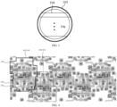
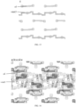
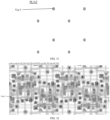
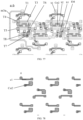
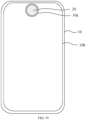
- FIG. 1 is a top view of a display panel according to some embodiments of the present disclosure.
- the base substrate 101 of the display panel 10 is provided with a first display region 10a.
- the first display region 10a is configured to be provided with an optical sensor.
- the optical sensor is a front camera, and the first display region 10a is referred to as a full display with camera (FDC) region.
- FDC full display with camera
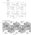
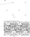
- FIG. 2 is a partial schematic structural diagram of the display panel shown in FIG. 1 .
- the display panel 10 includes a base substrate 101, a plurality of pixel circuit groups 102, and a plurality of first signal lines 103 in one-to-one correspondence with the plurality of pixel circuit groups 102.
- the plurality of pixel circuit groups 102 are disposed in the first display region 10a and are arranged along a first direction X.
- At least one pixel circuit group 102 includes a plurality of first pixel circuits 1021 arranged along a second direction Y and a plurality of second pixel circuits 1022 arranged along the second direction Y
- the first direction X is perpendicular to the second direction Y.
- the first direction X is a pixel column direction
- the second direction Y is a pixel row direction.
- the plurality of first pixel circuits 1021 and the plurality of second pixel circuits 1022 in each pixel circuit group 102 are alternately arranged, and each of the plurality of first pixel circuits 1021 and the plurality of second pixel circuits 1022 includes a first boundary and a second boundary that extend along the second direction Y and are arranged in the first direction X.
- the arrangement direction of a first boundary 1021a and a second boundary 1021b of the first pixel circuit 1021 is opposite to the arrangement direction of a first boundary 1022a and a second boundary 1022b of the second pixel circuit 1022.
- the distance, in the first direction X, between the first boundary 1021a of the first pixel circuit 1021 and the first boundary 1022a of the second pixel circuit 1022 is greater than a first distance H1
- the distance, in the first direction X, between the second boundary 1021b of the first pixel circuit 1021 and the second boundary 1022b of the second pixel circuit 1022 is less than the first distance H1.
- the first distance H1 is the distance, in the first direction X, between the first boundary and the second boundary of the same pixel circuit.
- the first distance H1 is the distance, in the first direction X, between the first boundary and the second boundary of the first pixel circuit 1021 or the second pixel circuit 1022.
- the distance, in the first direction X, between the first boundary 1021a and the second boundary 1021b of the first pixel circuit 1021 is equal to the distance, in the first direction X, between the first boundary 1022a and the second boundary 1022b of the second pixel circuit 1022.
- the first boundary 1021a of the first pixel circuit 1021 corresponds to the first boundary 1022a of the second pixel circuit 1022
- the second boundary 1021b of the first pixel circuit 1021 corresponds to the second boundary 1022b of the second pixel circuit 1022.
- Two boundaries corresponding to each other means that the pixel circuits at the locations of the two boundaries are of the same structure, and the plurality of first pixel circuits 1021 and the plurality of second pixel circuits 1022 are designed in opposite directions. Assuming that the design direction of the first pixel circuits 1021 is a forward direction, then the design direction of the second pixel circuits 1022 is a reverse direction. Alternatively, assuming that the design direction of the first pixel circuits 1021 is a reverse direction, then the design direction of the second pixel circuits 1022 is a forward direction.
- the first boundary or the second boundary of the pixel circuit 1021 is used to describe and show the strict boundary division of the pixel circuit 1021, and the boundary of the pixel circuit 1021 is not exactly the rectangle shown in FIG. 1 .
- the boundary of the pixel circuit 1021 is a boundary that forms the smallest region of a plurality of patterns of the pixel circuit 1021. The smallest region is the smallest circumscribed pattern of the pixel circuit. Therefore, the first boundary and the second boundary of the pixel circuit 1021 are respectively two boundaries that are farthest in the first direction X.
- the second boundaries 1021b of the plurality of first pixel circuits 1021 and the second boundaries 1022b of the plurality of second pixel circuits 1022 are all disposed between the extension line of the first boundary 1021a of the first pixel circuit 1021 and the extension line of the first boundary 1022a of the second pixel circuit 1022.
- each first signal line 103 is of an integral structure and is connected to each of the plurality of first pixel circuits 1021 and the plurality of second pixel circuits 1022 in the corresponding pixel circuit group 102. In this way, each first signal line 103 provides signals for all pixel circuits disposed in the first display region 10a in the corresponding pixel circuit group 102.
- the first signal line 103 being of an integral structure refers to that the portion of the first signal line 103 in the first display region 10a is disposed in only one film layer of the display panel 10, without the need to cross layers.
- the plurality of first pixel circuits 1021 and the plurality of second pixel circuits 1022 are offset in the first direction X and are designed in opposite directions, there is a certain offset between the connection positions of the first signal line 103 and the plurality of first pixel circuits 1021 and the connection positions of the first signal line 103 and the plurality of second pixel circuits 1022 in the first direction X.
- each first signal line 103 is connected to each first pixel circuit 1021 in the corresponding pixel circuit group 102 at a first connection (i.e., the connection position of the first signal line 103 and the first pixel circuit 1021 is referred to as the first connection), and the first signal line 103 is connected to each second pixel circuit 1022 in the corresponding pixel circuit group 102 at a second connection (i.e., the connection position of the first signal line 103 and the second pixel circuit 1022 is referred to as the second connection).
- the position of the first connection in the first pixel circuit 1021 corresponds to the position of the second connection in the second pixel circuit 1022. That is, the distance w1 between the first connection and the first boundary of the first pixel circuit 1021 is equal to the distance w1 between the second connection and the first boundary of the second pixel circuit 1022.
- the distance between the first connection and the second connection in the first direction X is smaller, for example, in the second direction Y, the first connection and the second connection are in the same horizontal line or near the same horizontal line.
- the distance, in the first direction X, between the first connection and the second connection is less than a second distance H2.
- the second distance H2 is the distance, in the first direction X, between the first boundary 1021a of the first pixel circuit 1021 and the second boundary 1022b of the second pixel circuit 1022 (i.e., the offset distance between the first pixel circuit 1021 and the second pixel circuit 1022 in the first direction X).
- the first signal line 103 can be directly connected to the pixel circuits (the plurality of first pixel circuits 1021 and the plurality of second pixel circuits 1022) in the pixel circuit group 102, without the need to design connection holes between adjacent pixel circuits and implement the connection by a trace layer.
- the number of connection holes to be designed in the layout can be reduced, and there is sufficient space to design a smaller number of connection holes for signal transmission even if the requirement on the PPI of the display panel is high.
- the embodiments of the present disclosure provide a display panel.
- the plurality of first pixel circuits and the plurality of second pixel circuits in each pixel circuit group in the display panel are alternately arranged, the plurality of first pixel circuits and the plurality of second pixel circuits in each pixel circuit group are designed in opposite directions, and the plurality of first pixel circuits and the plurality of second pixel circuits are offset in the first direction.
- the distance between the first connection of the first pixel circuit and the second connection of the second pixel circuit in the first direction is smaller.
- the first signal line is directly connected to the first connection and the second connection, without the need to design connection holes between adjacent pixel circuits and implement the connection by a trace layer.
- the number of connection holes to be designed in the layout can be reduced, and there is sufficient space to design a smaller number of connection holes for signal transmission even if the requirement on the PPI of the display panel is high.
- the first signal line 103 is a light-emitting control signal line EM.
- the plurality of pixel circuit groups 102 at least include a first pixel circuit group 102a and a second pixel circuit group 102b arranged in the first direction X.
- the distance, in the first direction X, between the first boundary 1022a of the second pixel circuit 1022 in the first pixel circuit group 102a and the first boundary 1021a of the first pixel circuit 1021 in the second pixel circuit group 102b is less than the second distance H2. That is, the second pixel circuit 1022 in the first pixel circuit group 102a and the first pixel circuit 1021 in the second pixel circuit 1022 are closer in the first direction X.
- the display panel 10 further includes a plurality of second signal lines 104 disposed in the first display region 10a.
- Each second signal line 104 is connected to the second pixel circuits 1022 in the first pixel circuit group 102a and the first pixel circuits 1021 in the second pixel circuit group 102b.
- the second signal line 104 provides signals for the second pixel circuits 1022 in the first pixel circuit group 102a and the first pixel circuits 1021 in the second pixel circuit group 102b at the same time.
- this second signal line 104 is a first reset power line vinit1.
- each of the plurality of second signal lines 104 is connected to the first connection trace 105.
- both ends of each second signal line 104 are connected to the first connection trace.
- Each second signal line 104 transmits a signal received from the first connection trace 105 to a pixel circuit connected to the second signal line 104.
- the signals transmitted by the plurality of second signal lines 104 to which the first connection trace 105 is connected are the same.
- the same signals mean that the signals have the same type and potential.
- the display panel 10 further includes a plurality of third signal lines 106 in one-to-one correspondence with the plurality of pixel circuit groups 102.
- Each third signal line 106 is connected to the plurality of first pixel circuits 1021 and the plurality of second pixel circuits 1022 in the corresponding pixel circuit group 102, such that each third signal line 106 provides signals for the first pixel circuits 1021 and the second pixel circuits 1022 in the corresponding pixel circuit group 102.
- the third signal line 106 may be or may not be of an integral structure.
- the third signal line 106 being of an integral structure means that the portion of the third signal line 106 in the first display region 10a is disposed in only one film layer of the display panel, without the need to cross layers.
- the third signal line 106 being not of an integral structure means that the portion of the third signal line 106 in the first display region 10a requires a cross-layer design, and the film layer in which the third signal line 106 is disposed is a metal layer.
- Each third signal line 106 is connected to the first pixel circuits 1021 and the second pixel circuits 1022 in the corresponding pixel circuit group 102.
- the signal transmitted by the third signal line 106 is different from the signal transmitted by the first signal line 103.
- Different signals mean that the signals at least have different types.
- the first signal line 103 is a light-emitting control signal line EM
- the signal transmitted is a light-emitting control EM signal
- the signal transmitted by the third signal line 106 is not an EM signal.
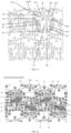
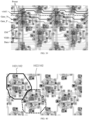
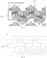
- each of the plurality of first pixel circuits 1021 and the plurality of second pixel circuits 1022 in each pixel circuit group 102 includes eight transistors and one storage capacitor Cst (i.e., 8T1C), such as shown in FIG. 4 .
- FIG. 4 only shows up to the first source-drain layer, but does not show the film layers on the side of the first source-drain layer away from the base substrate 101.
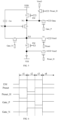
- FIG. 5 is an equivalent circuit diagram of a pixel circuit in the display panel shown in FIG. 4 .
- the pixel circuit includes a first transistor T1, a second transistor T2, a third transistor T3, a fourth transistor T4, a fifth transistor T5, a sixth transistor T6, a seventh transistor T7, an eighth transistor T8, and a storage capacitor Cst.
- a gate of the first transistor T1 is connected to a first reset signal line Preset in the display panel, a first electrode of the first transistor T1 is connected to a first reset power line vinit1, and a second electrode of the first transistor T1 is connected to a third node N3.
- the first transistor T1 is also referred to as a reset transistor.
- a gate of the second transistor T2 is connected to a first gate signal line Gate_N in the display panel, a first electrode of the second transistor T2 is connected to the third node N3, and a second electrode of the second transistor T2 is connected to a second node N2.
- the second transistor T2 is also referred to as a compensation transistor.
- a gate of the third transistor T3 is connected to the second node N2, a first electrode of the third transistor T3 is connected to a first node N1, and a second electrode of the third transistor T3 is connected to the third node N3.
- This third transistor T3 is also referred to as a driving transistor.
- a gate of the seventh transistor T7 is connected to a second reset signal line Preset_H in the display panel, a first electrode of the seventh transistor T7 is connected to a second reset power line vinit2, and a second electrode of the seventh transistor T7 is connected to the light-emitting unit.
- the seventh transistor T7 is a reset transistor in the pixel circuit.
- a gate of the eighth transistor T8 is connected to the second reset signal line Preset_H, a first electrode of the eighth transistor T8 is connected to a third reset power line vinit3 in the display panel, and a second electrode of the eighth transistor T8 is connected to the first node N1.
- the eighth transistor T8 is a reset transistor in the pixel circuit.
- One terminal of the storage capacitor Cst is connected to the driving power line VDD, and the other terminal of the storage capacitor Cst is connected to the second node N2.
- the second transistor T2 is an N-type transistor.
- the first transistor T1, the third transistor T3, the fourth transistor T4, the fifth transistor T5, the sixth transistor T6, the seventh transistor T7, and the eighth transistor T8 are all P-type transistors.
- FIG. 6 is a timing diagram of various signal lines in a pixel circuit according to some embodiments of the present disclosure. As shown in FIG. 6 :
- the potential of a first reset signal provided by the first reset signal line Preset, the potential of a second gate driving signal provided by the second gate signal line Gate_P, and the potential of a light-emitting control signal provided by the light-emitting control signal line EM are the first potential; and the potential of a first gate driving signal provided by the first gate signal line Gate_N and the potential of a second reset signal provided by the second reset signal line Preset_H are the second potential. Accordingly, the seventh transistor T7 and the eighth transistor T8 are turned on. The first transistor T1, the second transistor T2, the third transistor T3, the fourth transistor T4, the fifth transistor T5, and the sixth transistor T6 are turned off.
- the second reset power signal at the second potential provided by the second reset power line vinit2 can be transmitted to an anode of the light-emitting unit through the turned-on seventh transistor T7
- the third reset power signal at the second potential provided by the third reset power line vinit3 can be transmitted to the first node N1 through the turned-on eighth transistor T8, thereby resetting the anode of the light-emitting unit and the first node N1.
- the potential of the first reset signal provided by the first reset signal line Preset jumps to the second potential
- the potential of the first gate driving signal provided by the first gate signal line Gate_N jumps to the first potential
- the potential of the light-emitting control signal provided by the light-emitting control signal line EM maintains at the first potential. Accordingly, the first transistor T1 and the second transistor T2 are turned on, and the fourth transistor T4, the fifth transistor T5, the sixth transistor T6, the seventh transistor T7, and the eighth transistor T8 are turned off.
- the data signal at the first potential can be transmitted to the first node N1 through the turned-on fourth transistor T4, and then transmitted to the third node N3 through the turned-on third transistor T3, and the second transistor T2 adjusts the potential of the second node N2 based on the potential of the third node N3.
- the reset power signal at the second potential provided by the first reset power line vinit1 can be transmitted to the second node N2 through the turned-on first transistor T1 and second transistor T2, thereby resetting the second node N2.
- the potential of the first reset signal provided by the first reset signal line Preset jumps to the second potential
- the second reset signal provided by the second reset signal line Prese_H maintains at the second potential
- the potential of the second gate driving signal provided by the second gate signal line Gate_P jumps to the first potential
- the first gate signal line Gate_N maintains at the second potential
- the potential of the light-emitting control signal provided by the light-emitting control signal line EM maintains at the first potential.
- the potential of the second node N2 maintains at the second potential.
- the second transistor T2, the third transistor T3, and the fourth transistor T4 are turned on, and the first transistor T1, the fifth transistor T5, the sixth transistor T6, the seventh transistor T7, and the eighth transistor T8 are turned off.
- the data signal provided by the data signal line Data can be transmitted to the second node N2 through the turned-on fourth transistor T4, third transistor T3, and second transistor T2 in sequence.
- the potential of the first reset signal provided by the first reset signal line Preset maintains at the second potential
- the second reset signal provided by the second reset signal line Prese_H maintains at the second potential
- the potential of the second gate driving signal provided by the second gate signal line Gate_P jumps to the first potential
- the first gate signal line Gate_N jumps to the first potential
- the potential of the light-emitting signal provided by the light-emitting control signal line EM jumps to the first potential.
- the potential of the second node N2 maintains at the second potential of the data signal line Data.
- the third transistor T3, the fifth transistor T5, and the sixth transistor T6 are turned on, and the first transistor T1, the second transistor T2, the fourth transistor T4, the seventh transistor T7, and the eighth transistor T8 are turned off.
- the driving power signal provided by the driving power line VDD can be transmitted to the first node N1 through the turned-on fifth transistor T5, and the third transistor T3 can transmit a driving current to the third node N3 based on the potential of the second node N2 and the potential transmitted to the first node N1.
- the driving current can be transmitted again to the anode of the light-emitting unit through the turned-on sixth transistor T6, a voltage difference is generated between the anode of the light-emitting unit and a cathode layer, and the light-emitting unit emits light.
- the cathode layer is connected to the driving power line VSS.
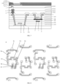
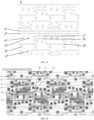
- FIG. 7 is a sectional view of a display panel according to some embodiments of the present disclosure.
- the display panel 10 includes an active layer a, a first gate insulating layer GI1, a first gate layer b, a second gate insulating layer GI2, a second gate layer c, a third gate insulating layer GI3, an oxide layer d, a fourth gate insulating layer GI4, a third gate layer e, an interlayer dielectric layer ILD, and a first source-drain layer f that constitute the pixel circuit and are sequentially stacked in the direction away from the base substrate 101.
- the display panel 10 further includes a passivation layer PVX, a first trace layer g, a first planarization layer PLN1, a second trace layer h, a second planarization layer PLN2, a second source-drain layer i, and a third planarization layer PLN3 that constitute the pixel circuit and are sequentially stacked in the direction away from the first source-drain layer f.
- the first signal line 103 is disposed in the first gate layer b
- the third signal line 106 is disposed in the third gate layer e.
- FIG. 7 is only intended to show the lamination relationship of the various film layers, but not intended to indicate a specific sectional view of the display panel and the connection relationship of the transistors of the pixel circuit in the display panel.
- FIG. 7 shows one oxide thin film transistor and one LTPS thin film transistor.
- the oxide thin film transistor is the second transistor T2
- the LTPS thin film transistor is the sixth transistor T6.
- the second transistor T2 is a dual gate transistor.
- the second gate layer c includes a gate pattern of a bottom gate of the second transistor T2.
- the oxide layer d includes an oxide pattern of the second transistor T2.
- the third gate layer e includes a gate pattern of a top gate of the second transistor T2.
- the first transistor T1, the third transistor T3, the fourth transistor T4, the fifth transistor T5, the sixth transistor T6, the seventh transistor T7, and the eighth transistor T8 are LTPS thin film transistors, and thus the first transistor T1, the third transistor T3, the fourth transistor T4, the fifth transistor T5, the sixth transistor T6, the seventh transistor T7, and the eighth transistor T8 are composed of the active layer a, the first gate layer b, and the first source-drain layer f.
- the active layer a includes an active pattern of the first transistor T1, an active pattern of the third transistor T3, an active pattern of the fourth transistor T4, an active pattern of the fifth transistor T5, an active pattern of the sixth transistor T6, an active pattern of the seventh transistor T7, and an active pattern of the eighth transistor T8.
- the first gate layer b includes a gate pattern of the first transistor T1, a gate pattern of the third transistor T3, a gate pattern of the fourth transistor T4, a gate pattern of the fifth transistor T5, a gate pattern of the sixth transistor T6, a gate pattern of the seventh membrane transistor T7, and a gate pattern of the eighth transistor T8.
- the light-emitting control signal line EM is disposed in the first gate layer b
- the first reset power line vinit1 is disposed in the first source-drain layer f
- the third reset power line vinit3 is disposed in the third gate layer e. That is, in the embodiments, the third signal line 106 (the third reset power line vinit3) is of an integral structure.
- transverse signal lines e.g., the first gate signal line Gate_N, the second gate signal line Gate_P, the first reset signal line Preset, and the second reset signal line Preset_H
- the longitudinal signal lines e.g., the data signal line Data and the driving power line VDD
- the transverse signal lines mainly provide signals for the plurality of pixel circuits arranged in the transverse direction
- the longitudinal signal lines mainly provide signals for the plurality of pixel circuits arranged in the longitudinal direction.
- the various film layers in the case that the pixel circuit includes eight transistors are introduced by describing each layer and a step-by-step stacking of layers.
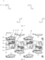
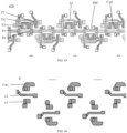
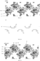
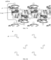
- FIG. 8 is a partial schematic diagram of an active layer in a display panel according to some embodiments of the present disclosure.
- the active layer a is provided with structures in a curved or bent shape, the active layer a includes active patterns (channel regions) and doped region patterns (source-drain doped regions) of the various transistors, and the active patterns and the doped region patterns of the various transistors in the same pixel circuit are arranged integrally.
- the active layer a may include a low-temperature polysilicon layer integrally formed, and the source region and the drain region may be conducted by doping or the like to electrically connect various structures. That is, the semiconductor layers of the transistors of the various pixel circuits are an integral pattern formed of p-silicon, and the transistors in the same pixel circuit include doped region patterns (i.e., source regions and drain regions) and active patterns, and the active patterns of different transistors are spaced apart from each other.
- doped region patterns i.e., source regions and drain regions
- the active layer a is made of amorphous silicon, polysilicon, oxide semiconductor material, or the like. It should be noted that the source region and the drain region described above may be regions doped with n-type impurities or p-type impurities.
- the display panel includes a first gate insulating layer disposed on the side of the active layer a away from the base substrate 101 for insulating the active layer a from the first gate layer b formed subsequently.
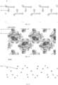
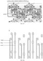
- FIG. 9 is a partial schematic diagram of a first gate layer in a display panel according to some embodiments of the present disclosure.
- FIG. 10 is a partial schematic diagram of superposition of an active layer and a first gate layer in a display panel according to some embodiments of the present disclosure.
- the first gate layer b in the display panel shown in FIG. 9 and FIG. 10 is disposed on a first gate insulating layer, so as to be insulated from the active layer a.
- the first gate layer b includes the second storage capacitance electrode Cst2, the light-emitting control signal line EM, a gate layer pattern b1 of the first reset signal line Preset that provides the first reset signal for the gate of the first transistor T1, a gate layer pattern b2 of the second gate signal line Gate_P, and a gate layer pattern b3 of the second reset signal line Preset_H that provides the second reset signal for the gate of the eighth transistor T8.
- the gate of the first transistor T1 is the overlapping portion of the gate layer pattern b1 of the first reset signal line Preset and the active layer a.
- the gate of the third transistor T3 is the second storage capacitance electrode Cst2.
- the gate of the fourth transistor T4 is the overlapping portion of the gate layer pattern b2 of the second gate signal line Gate_P and the active layer a.
- the gate of the fifth transistor T5 and the gate of the sixth transistor T6 are the overlapping portions of the light-emitting control signal line EM and different regions of the active layer a, respectively.
- the seventh transistor T7 and the eighth transistor T8 are the overlapping portions of the gate layer pattern b3 of the second reset signal line Preset_H and different regions of the active layer a, respectively.
- the dashed rectangular boxes in FIG. 10 illustrate the overlapping portions of the first gate layer b and the active layer a.
- the active layers a on two sides of the channel region are conducted by processes such as ion doping and serve as the first electrode and the second electrode of the transistor.
- the source and the drain of the transistor are structurally symmetrical, and thus the source and the drain of the transistor are physically indistinguishable.
- one electrode of the transistor is directly described as the first electrode, and the other electrode is described as the second electrode. Therefore, the first electrodes and the second electrodes of all or some of the transistors in the embodiments of the present disclosure are interchangeable as needed.
- the light-emitting control signal line EM is of an integral structure disposed in the first gate layer b. Additionally, a second gate insulating layer is formed on the first gate layer b for insulating the first gate layer b from a second gate layer c formed subsequently.
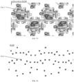
- FIG. 11 is a partial schematic diagram of a second gate layer in a display panel according to some embodiments of the present disclosure
- FIG. 12 is a partial schematic diagram of superposition of an active layer, a first gate layer, and a second gate layer in a display panel according to some embodiments of the present disclosure.
- the second gate layer c includes a first storage capacitance electrode Cst1 and a bottom gate pattern c1 of the second transistor T2 which is disposed in the second gate layer c.
- the first storage capacitance electrode Cst1 disposed in the second gate layer c is at least partially overlapped with the second storage capacitance electrode Cst2 disposed in the first gate layer b to form the storage capacitor Cst.
- the bottom gate pattern c1 is also used as a portion of the first gate signal line Gate_N that is disposed in the second gate layer c.
- a third gate insulating layer is formed on the second gate layer c for insulating the second gate layer c from an oxide layer d formed subsequently.
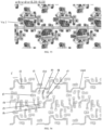
- FIG. 13 is a partial schematic diagram of an oxide layer in a display panel according to some embodiments of the present disclosure
- FIG. 14 is a partial schematic diagram of superposition of an active layer, a first gate layer, a second gate layer, and an oxide layer in a display panel according to some embodiments of the present disclosure.
- the oxide layer d includes an oxide pattern d1 for forming the second transistor T2.
- a fourth gate insulating layer is formed on the oxide layer d for insulating the oxide layer d from a third gate layer e formed subsequently.
- FIG. 15 is a partial schematic diagram of a third gate layer in a display panel according to some embodiments of the present disclosure
- FIG. 16 is a partial schematic diagram of superposition of an active layer, a first gate layer, a second gate layer, an oxide layer, and a third gate layer in a display panel according to some embodiments of the present disclosure.
- the third gate layer e includes a top gate pattern e1 of the second transistor T2 that is disposed in the third gate layer e, and the third reset power line vinit3.
- the third reset power line vinit3 is of an integral structure disposed in the third gate layer e.
- FIG. 17 is a partial schematic diagram of a first interlayer dielectric layer in a display panel according to some embodiments of the present disclosure
- FIG. 18 is a partial schematic diagram of superposition of an active layer, a first gate layer, a second gate layer, an oxide layer, a third gate layer, and a first interlayer dielectric layer in a display panel according to some embodiments of the present disclosure
- FIG. 19 is a partial schematic diagram of a second interlayer dielectric layer in a display panel according to some embodiments of the present disclosure.
- 20 is a partial schematic diagram of superposition of an active layer, a first gate layer, a second gate layer, an oxide layer, a third gate layer, a first interlayer dielectric layer, and a second interlayer dielectric layer in a display panel according to some embodiments of the present disclosure.
- fill patterns are used to represent the vis in FIG. 17 to FIG. 20 .
- Other regions without a fill pattern represent regions of the interlayer dielectric layer where materials are provided.
- the vias formed in the interlayer dielectric layer are configured to connect the film layers formed subsequently and the film layer on the side of the interlayer dielectric layer close to the base substrate 101. That is, the vias are used for connecting film layers.
- FIG. 21 is a partial schematic diagram of a first source-drain layer in a display panel according to some embodiments of the present disclosure
- FIG. 22 is a partial schematic diagram of superposition of an active layer, a first gate layer, a second gate layer, an oxide layer, a third gate layer, a first interlayer dielectric layer, a second interlayer dielectric layer, and a first source-drain layer in a display panel according to some embodiments of the present disclosure.
- the first source-drain layer f includes:
- FIG. 23 is a partial schematic diagram of a passivation layer in a display panel according to some embodiments of the present disclosure
- FIG. 24 is a partial schematic diagram of superposition of an active layer, a first gate layer, a second gate layer, an oxide layer, a third gate layer, a first interlayer dielectric layer, a second interlayer dielectric layer, a first source-drain layer, and a passivation layer in a display panel according to some embodiments of the present disclosure.
- fill patterns are used to represent the vias in FIG. 23 to FIG. 24 .
- Other regions without a fill pattern represent the regions of the passivation layer where materials are provided.
- the vias formed in the passivation layer are configured to connect the film layers formed subsequently and the film layer on the side of the passivation layer close to the base substrate 101. That is, the vias are vias for connecting film layers.
- FIG. 25 is a partial schematic diagram of a first trace layer in a display panel according to some embodiments of the present disclosure
- FIG. 26 is a partial schematic diagram of superposition of an active layer, a first gate layer, a second gate layer, an oxide layer, a third gate layer, a first interlayer dielectric layer, a second interlayer dielectric layer, a first source-drain layer, a passivation layer, and a trace layer in a display panel according to some embodiments of the present disclosure.
- the first trace layer g includes:
- fill patterns are used to represent the vias in FIG. 27 to FIG. 28 .
- Other regions without a fill pattern represent the regions of the first planarization layer where materials are provided.
- the vias formed in the first planarization layer are configured to connect the film layers formed subsequently and the film layer on the side of the first planarization layer close to the base substrate 101. That is, the vias are used for connecting film layers.
- FIG. 31 is a partial schematic diagram of a second planarization layer in a display panel according to some embodiments of the present disclosure
- FIG. 32 is a partial schematic diagram of superposition of an active layer, a first gate layer, a second gate layer, an oxide layer, a third gate layer, a first interlayer dielectric layer, a second interlayer dielectric layer, a first source-drain layer, a passivation layer, a first trace layer, a first planarization layer, a second trace layer, and a second planarization layer in a display panel according to some embodiments of the present disclosure.
- fill patterns are used to represent the vias in FIG. 30 and FIG. 31 .
- Other regions without a fill pattern represent the regions of the second planarization layer where materials are provided.
- the vias formed in the second planarization layer are configured to connect the film layers formed subsequently and the film layer on the side of the second planarization layer close to the base substrate 101. That is, the vias are used for connecting film layers.
- FIG. 33 is a partial schematic diagram of a second source-drain layer in a display panel according to some embodiments of the present disclosure
- FIG. 34 is a partial schematic diagram of superposition of an active layer, a first gate layer, a second gate layer, an oxide layer, a third gate layer, a first interlayer dielectric layer, a second interlayer dielectric layer, a first source-drain layer, a passivation layer, the first trace layer, a first planarization layer, a second trace layer, a second planarization layer, and a second source-drain layer in a display panel according to some embodiments of the present disclosure.
- the second source-drain layer i includes a sixteenth source-drain pattern i1.
- the sixteenth source-drain pattern i1 is connected to the seventh transistor T7 and an anode layer of a light-emitting unit formed subsequently.
- FIG. 35 is a partial schematic diagram of a third planarization layer in a display panel according to some embodiments of the present disclosure.
- fill patterns are used to represent the vias in FIG. 35 and FIG. 36 .
- Other regions without a fill pattern represent the regions of the third planarization layer where materials are provided.
- the vias formed in the third planarization layer are configured to connect the film layers formed subsequently and the film layer on the side of the third planarization layer close to the base substrate 101. That is, the vias are used for connecting film layers.
- FIG. 37 is a partial schematic diagram of an anode layer in a display panel according to some embodiments of the present disclosure
- FIG. 38 is a partial schematic diagram of superposition of an active layer, a first gate layer, a second gate layer, an oxide layer, a third gate layer, a first interlayer dielectric layer, a second interlayer dielectric layer, a first source-drain layer, a passivation layer, a first trace layer, a first planarization layer, a second trace layer, a second planarization layer, a second source-drain layer, a third planarization layer, and a anode layer in a display panel according to some embodiments of the present disclosure.
- the anode of the light-emitting unit is connected to the fifteenth source-drain pattern i1 of the second source-drain layer i through the via 6 in the third planarization layer.
- the various patterns shown in FIG. 37 and FIG. 38 are only intended to illustrate the position of the anode and do not indicate the actual shape of the anode.
- each of the plurality of first pixel circuits 1021 and the plurality of second pixel circuits 1022 in each pixel circuit group 102 includes seven transistors and one storage capacitor Cst (i.e., 7T1C), such as shown in FIG. 39 and FIG. 40 .
- FIG. 40 only shows up to the first source-drain layer, but does not show the film layers on the side of the first source-drain layer away from the base substrate 101.
- a gate of the first transistor T1 is connected to a first reset signal line Preset, a first electrode of the first transistor T1 is connected to a first reset power line vinit1, and a second electrode of the first transistor T1 is connected to a second node N2.
- the first transistor T1 is also referred to as a reset transistor.
- a gate of the second transistor T2 is connected to a first gate signal line Gate_N, a first electrode of the second transistor T2 is connected to a third node N3, and a second electrode of the second transistor T2 is connected to the second node N2.
- the second thin film transistor T2 is also referred to as a compensation transistor.
- a gate of the third transistor T3 is connected to the second node N2, a first electrode of the third transistor T3 is connected to a first node N1, and a second electrode of the third transistor T3 is connected to the third node N3.
- the third transistor T3 is also referred to as a driving transistor.
- a gate of the fourth transistor T4 is connected to a second gate signal line Gate_P, a first electrode of the fourth transistor T4 is connected to a data signal line Data, and a second electrode of the fourth transistor T4 is connected to the first node N1.
- the fourth transistor T4 is a data-writing transistor in the pixel circuit.
- a gate of the sixth transistor T6 is connected to the light-emitting control signal line EM, a first electrode of the sixth transistor T6 is connected to the third node N3, and a second electrode of the sixth transistor T6 is connected to an anode of the light-emitting unit.
- the sixth transistor T6 is also referred to as a light-emitting control transistor.
- a gate of the seventh transistor T7 is connected to the second gate signal line Gate_P, a first electrode of the seventh transistor T7 is connected to the first reset power line vinit1, and a second electrode of the seventh transistor T7 is connected to the anode of the light-emitting unit.
- the seventh transistor T7 is a reset transistor in the pixel circuit.
- the storage capacitor Cst includes two capacitance plates Cstl and Cst2, and in the embodiments of the present disclosure, the capacitance plate Cst1 is referred to as one terminal, a first terminal, or a first storage capacitance electrode of the storage capacitor Cst, and the capacitance plate Cst2 is referred to as the other storage capacitance electrode, a second storage capacitance electrode, or a second storage capacitance electrode of the storage capacitor Cst.
- the third signal line 106 is a second gate signal line Gate_P. That is, in the case that the pixel circuit includes seven transistors and one storage capacitor Cst, the third signal line 106 is the second gate signal line Gate_P, and the second gate signal line Gate_P provides second gate signals for the plurality of first pixel circuits 1021 and the plurality of second pixel circuits 1022 in one pixel circuit group 102.
- the first transistor T1 and the second transistor T2 are N-type transistors
- the third transistor T3, the fourth transistor T4, the fifth transistor T5, the sixth transistor T6, and the seventh transistor T7 are P-type transistors.
- each N-type transistor is an oxide thin film transistor
- each P-type transistor is an LTPS thin film transistor.
- the oxide material includes IGZO, i.e., the oxide thin film transistor is an IGZO thin film transistor.
- the pixel circuit consisting of the seven transistors is also referred to as an LTPO pixel circuit.
- a display panel having the LTPO pixel circuit is also referred to as an LTPO display panel.
- FIG. 42 is a timing diagram of signal lines in another pixel circuit according to some embodiments of the present disclosure.
- the potential of a reset signal provided by the first reset signal line Preset, the potential of a second gate driving signal provided by the second gate signal line Gate_P, and the potential of a light-emitting control signal provided by the light-emitting control signal line EM are all the first potential, and the potential of a first gate driving signal provided by the first gate signal line Gate_N is the second potential.
- the first transistor T1 is turned on, and the second transistor T2, the fourth transistor T4, the fifth transistor T5, the sixth transistor T6, and the seventh transistor T7 are turned off.
- the reset power signal at the second potential provided by the first reset power line vinit1 can be transmitted to the second node N2 through the turned-on first transistor T1, thereby resetting the second node N2.
- a compensation stage t2 the potential of the reset signal provided by the first reset signal line Preset and the potential of the second gate driving signal provided by the second gate signal line Gate_P jump to the second potential, the potential of the first gate driving signal provided by the first gate signal line Gate_N jumps to the first potential, and the potential of the light-emitting control signal provided by the light-emitting control signal line EM maintains at the first potential.
- the potential of the second node N2 maintains at the second potential. Accordingly, the second transistor T2, the third transistor T3, the fourth transistor T4, and the seventh transistor T7 are turned on, and the first transistor T1, the fifth transistor T5, and the sixth transistor T6 are turned off.
- the data signal at the first potential can be transmitted to the first node N1 through the turned-on fourth transistor T4, and is then transmitted to the third node N3 through the turned-on third transistor T3, and the second transistor T2 adjusts the potential of the second node N2 based on the potential of the third node N3.
- the reset power signal at the second potential provided by the first reset power line vinit1 can be transmitted to the light-emitting unit a2 through the turned-on seventh transistor T7, thereby resetting the light-emitting unit.
- the potential of the reset signal provided by the first reset signal line Preset maintains at the second potential
- the potential of the second gate driving signal provided by the second gate signal line Gate_P jumps to the first potential
- the potential of the first gate driving signal provided by the first gate signal line Gate_N jumps to the second potential.
- the potential of the second node N2 maintains at the second potential. Accordingly, the third transistor T3, the fifth transistor T5, and the sixth transistor T6 are turned on, and the first transistor T1, the second transistor T2, the fourth transistor T4, and the seventh transistor T7 are turned off.
- the driving power signal provided by the driving power line VDD can be transmitted to the first node N1 through the turned-on fifth transistor T5, and the third transistor T3 can transmit a driving current to the third node N3 based on the potential of the second node N2 and the potential transmitted to the first node N1. Then, the driving current can be transmitted again to an anode pattern of the light-emitting unit through the turned-on sixth transistor T6, a voltage difference is generated between the anode pattern of the light-emitting unit and a cathode layer, and the light-emitting unit emits light.
- the cathode layer is connected to the driving power line VSS.
- the first signal line 103 is disposed in the first gate layer b, and the third signal line 106 includes a first portion, a second portion, and a third portion that are connected in sequence.
- An orthographic projection of the first portion on the base substrate 101 is at least partially overlapped with an orthographic projection of the first pixel circuit 1021 on the base substrate 101, an orthographic projection of the second portion on the base substrate 101 is not overlapped with the orthographic projection of the first pixel circuit 1021 on the base substrate 101 and the orthographic projection of the second pixel circuit 1022 on the base substrate 101, and an orthographic projection of the third portion on the base substrate 101 is at least partially overlapped with the orthographic projection of the second pixel circuit 1022 on the base substrate 101.
- the first portion and the third portion are disposed in the first gate layer b, and the second portion is disposed in the first source-drain layer f. That is, in this implementation, the third signal line 106 needs to cross layers, and both layers are metal layers.
- the first transistor T1 and the second transistor T2 are oxide thin film transistors, and thus the first transistor T1 and the second transistor T2 are composed of a second gate layer c, an oxide layer d, and a third gate layer e.
- the oxide layer d is made of IGZO.
- the first transistor T1 and the second transistor T2 are dual gate transistors.
- the second gate layer c includes a gate pattern of a bottom gate of the first transistor T1 and a gate pattern of a bottom gate of the second transistor T2.
- the oxide layer d includes an oxide pattern of the first transistor T1 and an oxide pattern of the second transistor T2.
- the third gate layer e includes a gate pattern of the bottom gate of the first transistor T1 and a gate pattern of a top gate of the second transistor T2.
- the third transistor T3, the fourth transistor T4, the fifth transistor T5, the sixth transistor T6, and the seventh transistor T7 are all LTPS thin film transistors, and thus the third transistor T3, the fourth transistor T4, the fifth transistor T5, the sixth transistor T6, and the seventh transistor T7 are composed of the active layer a, the first gate layer b, and the first source-drain layer f.
- the active layer a includes an active pattern of the third transistor T3, an active pattern of the fourth transistor T4, an active pattern of the fifth transistor T5, an active pattern of the sixth transistor T6, and an active pattern of the seventh transistor T7.
- the first gate layer b includes a gate pattern of the third transistor T3, a gate pattern of the fourth transistor T4, a gate pattern of the fifth transistor T5, a gate pattern of the sixth transistor T6, and a gate pattern of the seventh transistor T7.
- the light-emitting control signal line EM is disposed in the first gate layer b
- the first reset power line vinit1 is disposed in the first source-drain layer f
- the second gate signal line Gate_P is disposed in the first gate layer b and the first source-drain layer f.
- the various film layers in the case that the pixel circuit in FIG. 40 includes seven transistors are introduced by describing each layer and a step-by-step stacking of layers.
- FIG. 43 is a partial schematic diagram of an active layer in another display panel according to some embodiments of the present disclosure.
- the active layer a is provided with structures in a curved or bent shape, the active layer a includes the active patterns (channel regions) and the doped region patterns (source-drain doped regions) of the various transistors, and the active patterns and the doped region patterns of the various transistors in the same pixel circuit are arranged integrally.
- the active layer a may include a low-temperature polysilicon layer integrally formed, and the source region and the drain region may be conducted by doping or the like to electrically connect various structures. That is, the semiconductor layers of the transistors of the various pixel circuits are an integral pattern formed of p-silicon, and the transistors in the same pixel circuit include doped region patterns (i.e., source regions and drain regions) and active patterns, and the active patterns of different transistors are spaced apart from each other.
- doped region patterns i.e., source regions and drain regions
- the active layer a is made of amorphous silicon, polysilicon, oxide semiconductor material, or the like. It should be noted that the source region and the drain region described above may be regions doped with n-type impurities or p-type impurities.
- the display panel includes a first gate insulating layer disposed on the side of the active layer a away from the base substrate 101 for insulating the active layer a from the first gate layer b formed subsequently.
- FIG. 44 is a partial schematic diagram of a first gate layer in another display panel according to some embodiments of the present disclosure
- FIG. 45 is a partial schematic diagram of superposition of an active layer and a first gate layer in another display panel according to some embodiments of the present disclosure.
- the first gate layer b in the display panel shown in FIG. 44 and FIG. 45 is disposed on the first gate insulating layer, so as to be insulated from the active layer a.
- the first gate layer b includes the second storage capacitance electrode Cst2, the light-emitting control signal line EM, and a gate layer pattern b1 of the second gate signal line Gate_P.
- the overlapping portions of the first gate layer b and the active layer a constitute the gates of the various transistors.
- the gate of the third transistor T3 is the second storage capacitance electrode Cst2.
- the gate of the fourth transistor T4 and the gate of the seventh transistor T7 are the overlapping portions of the gate layer pattern b2 of the second gate signal line Gate_P and different regions of the active layer a, respectively.
- the gate of the fifth transistor T5 and the gate of the sixth transistor T6 are the overlapping portions of the light-emitting control signal line EM and different regions of the active layer a, respectively.
- the dashed rectangular boxes in FIG. 45 illustrate the overlapping portions of the first gate layer b and the active layer a.
- the active layers a on two sides of the channel region are conducted by processes such as ion doping and serve as the first electrode and the second electrode of the transistor.
- the source and the drain of the transistor are structurally symmetrical, and thus the source and the drain of the transistor are physically indistinguishable.
- one electrode of the transistor is directly described as the first electrode, and the other electrode is described as the second electrode. Therefore, the first electrodes and the second electrodes of all or some of the transistors in the embodiments of the present disclosure are interchangeable as needed.
- the light-emitting control signal line EM is of an integral structure disposed in the first gate layer b. Additionally, a second gate insulating layer is formed on the first gate layer b for insulating the first gate layer b from a second gate layer c formed subsequently.
- FIG. 46 is a partial schematic diagram of a second gate layer in another display panel according to some embodiments of the present disclosure
- FIG. 47 is a partial schematic diagram of superposition of an active layer, a first gate layer, and a second gate layer in another display panel according to some embodiments of the present disclosure.
- the second gate layer c includes:
- a third gate insulating layer is formed on the second gate layer c for insulating the second gate layer c from the oxide layer d formed subsequently.
- FIG. 48 is a partial schematic diagram of an oxide layer in another display panel according to some embodiments of the present disclosure
- FIG. 49 is a partial schematic diagram of superposition of an active layer, a first gate layer, a second gate layer, and an oxide layer in another display panel according to some embodiments of the present disclosure.
- the oxide layer d includes an oxide pattern d1 for forming the first transistor T1 and the second transistor T2.
- the first transistor T1 and the second transistor T2 are connected, and thus the oxide pattern of the first transistor T1 and the oxide pattern of the second transistor T2 are of an integral structure.
- a fourth gate insulating layer is formed on the oxide layer d for insulating the oxide layer d from a third gate layer e formed subsequently.
- FIG. 50 is a partial schematic diagram of a third gate layer in another display panel according to some embodiments of the present disclosure.
- FIG. 51 is a partial schematic diagram of superposition of an active layer, a first gate layer, a second gate layer, an oxide layer, and a third gate layer in another display panel according to some embodiments of the present disclosure.
- FIG. 52 is a partial schematic diagram of a first interlayer dielectric layer in another display panel according to some embodiments of the present disclosure.
- FIG. 53 is a partial schematic diagram of superposition of an active layer, a first gate layer, a second gate layer, an oxide layer, a third gate layer, and a first interlayer dielectric layer in another display panel according to some embodiments of the present disclosure.
- FIG. 54 is a partial schematic diagram of a second interlayer dielectric layer in another display panel according to some embodiments of the present disclosure.
- fill patterns are used to represent the vias in FIG. 52 to FIG. 55 .
- Other regions without a fill pattern represent the regions of the interlayer dielectric layers where materials are provided.
- the vias formed in each of the interlayer dielectric layers are configured to connect the film layers formed subsequently and the film layer on the side of the interlayer dielectric layer close to the base substrate 101. That is, the vias are used for connecting film layers.
- FIG. 56 is a partial schematic diagram of a first source-drain layer in another display panel according to some embodiments of the present disclosure
- FIG. 57 is a partial schematic diagram of superposition of an active layer, a first gate layer, a second gate layer, an oxide layer, a third gate layer, a first interlayer dielectric layer, a second interlayer dielectric layer, and a first source-drain layer in another display panel according to some embodiments of the present disclosure.
- the first source-drain layer f includes:
- FIG. 60 is a partial schematic diagram of a first trace layer in another display panel according to some embodiments of the present disclosure
- FIG. 61 is a partial schematic diagram of superposition of an active layer, a first gate layer, a second gate layer, an oxide layer, a third gate layer, a first interlayer dielectric layer, a second interlayer dielectric layer, a first source-drain layer, a passivation layer, and a first trace layer in another display panel according to some embodiments of the present disclosure.
- the first trace layer g includes:
- FIG. 62 is a partial schematic diagram of a first planarization layer in another display panel according to some embodiments of the present disclosure.
- FIG. 63 is a partial schematic diagram of superposition of an active layer, a first gate layer, a second gate layer, an oxide layer, a third gate layer, a first interlayer dielectric layer, a second interlayer dielectric layer, a first source-drain layer, a passivation layer, a first trace layer, and a first planarization layer in another display panel according to some embodiments of the present disclosure.
- fill patterns are used to represent the vias in FIG. 62 and FIG. 63 .
- Other regions without a fill pattern represent the regions of the first planarization layer where materials are provided.
- the vias formed in the first planarization layer are configured to connect the film layers formed subsequently and the film layer on the side of the first planarization layer close to the base substrate 101. That is, the vias are used for connecting film layers.
- FIG. 64 is a partial schematic diagram of a second trace layer in another display panel according to some embodiments of the present disclosure
- FIG. 65 is a partial schematic diagram of superposition of an active layer, a first gate layer, a second gate layer, an oxide layer, a third gate layer, a first interlayer dielectric layer, a second interlayer dielectric layer, a first source-drain layer, a passivation layer, a first trace layer, a first planarization layer, and a second trace layer in another display panel according to some embodiments of the present disclosure.
- the second trace layer h includes a data signal line Data, a pattern h1 of the driving power line VDD that is disposed in the second trace layer h, and a pattern h2 connected to the anode layer of the light-emitting unit.
- FIG. 66 is a partial schematic diagram of a second planarization layer in another display panel according to some embodiments of the present disclosure.
- FIG. 67 is a partial schematic diagram of superposition of an active layer, a first gate layer, a second gate layer, an oxide layer, a third gate layer, a first interlayer dielectric layer, a second interlayer dielectric layer, a first source-drain layer, a passivation layer, a first trace layer, a first planarization layer, a second trace layer, and a second planarization layer in another display panel according to some embodiments of the present disclosure.
- fill patterns are used to represent the vias in FIG. 66 and FIG. 67 .
- Other regions without a fill pattern represent the regions of the second planarization layer where materials are provided.
- the vias formed in the second planarization layer are configured to connect the film layers formed subsequently and the film layer on the side of the second planarization layer close to the base substrate 101. That is, the vias are used for connecting film layers.
- FIG. 68 is a partial schematic diagram of a second source-drain layer in another display panel according to some embodiments of the present disclosure
- FIG. 69 is a partial schematic diagram of superposition of an active layer, a first gate layer, a second gate layer, an oxide layer, a third gate layer, a first interlayer dielectric layer, a second interlayer dielectric layer, a first source-drain layer, a passivation layer, a first trace layer, a first planarization layer, a second trace layer, a second planarization layer, and a second source-drain layer in another display panel according to some embodiments of the present disclosure.
- the second source-drain layer i includes an eleventh source-drain pattern i1 and a twelfth source-drain pattern i2.
- the eleventh source-drain pattern i1 is a pattern of the driving power line VDD that is disposed in the second source-drain layer i, and the eleventh source-drain pattern i1 is connected to the pattern h1 of the driving power line VDD that is disposed in the second trace layer h through a via in the second planarization layer.
- the twelfth source-drain pattern i2 is connected to the anode layer of the light-emitting unit, and is connected to the pattern h2 disposed in the second electrode layer through a via in the second planarization layer.
- FIG. 70 is a partial schematic diagram of a third planarization layer in another display panel according to some embodiments of the present disclosure.
- 71 is a partial schematic diagram of superposition of an active layer, a first gate layer, a second gate layer, an oxide layer, a third gate layer, a first interlayer dielectric layer, a second interlayer dielectric layer, a first source-drain layer, a passivation layer, a first trace layer, a first planarization layer, a second trace layer, a second planarization layer, a first source-drain layer, and a third planarization layer in another display panel according to some embodiments of the present disclosure.
- fill patterns are used to represent the vias in FIG. 70 and FIG. 71 .
- Other regions without a fill pattern represent the regions of the third planarization layer where materials are provided.
- the vias formed in the third planarization layer are configured to connect the film layers formed subsequently and the film layer on the side of the third planarization layer close to the base substrate 101. That is, the vias are used for connecting film layers.
- FIG. 72 is a partial schematic diagram of an anode layer in another display panel according to some embodiments of the present disclosure
- FIG. 73 is a partial schematic diagram of superposition of an active layer, a first gate layer, a second gate layer, an oxide layer, a third gate layer, a first interlayer dielectric layer, a second interlayer dielectric layer, a first source-drain layer, a passivation layer, a first trace layer, a first planarization layer, a second trace layer, a second planarization layer, a second source-drain layer, a third planarization layer, and an anode layer in another display panel according to some embodiments of the present disclosure.
- the anode layer of the light-emitting unit is connected to the twelfth source-drain pattern i2 of the second source-drain layer i through the via 6 in the third passivation layer.
- the various patterns shown in FIG. 72 and FIG. 73 are only intended to illustrate the position of the anode layer, but do not represent the actual shape of the anode layer.
- each target signal line m in the display panel 10 includes a first sub-signal line m1, a second sub-signal line m2, and a second connection trace m3.
- the target signal line m is a signal line providing signals along the second direction Y other than the first signal line 103, the second signal line 104, and the third signal line 106 in the display panel 10.
- the target signal line m includes the first gate signal line Gate_N, the second gate signal line Gate_P, the first reset signal line Preset, and the second reset signal line Preset_H.
- the target signal line m includes the first reset signal line Preset and the first gate signal line Gate_N.
- the first sub-signal line m1 is disposed in the first display region 10a, and the first sub-signal line m1 is connected to a plurality of first pixel circuits 1021 in one pixel circuit group 102.
- the second sub-signal line m2 is disposed in the first display region 10a, and the second sub-signal line m2 is connected to a plurality of second pixel circuits 1022 in one pixel circuit group 102.
- the plurality of second pixel circuits 1022 connected to the second sub-signal line m2 of each target signal line m and the plurality of first pixel circuits 1021 connected to the first sub-signal line m1 of the target signal line m belong to the same pixel circuit group 102.
- the second connection trace m3 is disposed in the second display region 10b, one end of the second connection trace m3 is connected to the first sub-signal line m1, and the other end of the second connection trace m3 is connected to the second sub-signal line m2. That is, the first sub-signal line m1 and the second sub-signal line m2 are connected by the second connection trace m3. Therefore, the signals provided by the first sub-signal line m1 for the plurality of first pixel circuits 1021 in the pixel circuit group 102 are the same as the signals provided by the second sub-signal line m2 for the plurality of second pixel circuits 1022 in the pixel circuit group 102.
- the first sub-signal line m1 includes a fourth portion m11 and a fifth portion m12 that are connected.
- An orthographic projection of the fourth portion m11 on the base substrate 101 is at least partially overlapped with an orthographic projection of the first pixel circuit 1021 on the base substrate 101, and an orthographic projection of the fifth portion m12 on the base substrate 101 is between an orthographic projections of two adjacent first pixel circuits 1021 on the base substrate 101.
- the second sub-signal line m2 includes a sixth portion m21 and a seventh portion m22 that are connected.
- An orthographic projection of the sixth portion m21 on the base substrate 101 is at least partially overlapped with an orthographic projection of the second pixel circuit 1022 on the base substrate 101, and an orthographic projection of the seventh portion m22 on the base substrate 101 is between the orthographic projections of two adjacent second pixel circuits 1022 on the base substrate 101.
- the fourth portion m11 and the sixth portion m21 are disposed in the same layer, and the fourth portion m11 and the sixth portion m21 are disposed in a metal layer, e.g., a gate layer or a source-drain layer.
- the fifth portion m12 and the seventh portion m22 are disposed in the same layer, and the fifth portion m12 and the seventh portion m22 are disposed in a trace layer, e.g., the first trace layer g. Therefore, referring to FIG. 75 , the fourth portion m11 and the fifth portion m12 are connected through a via in the insulating layer therebetween. Similarly, the sixth portion m21 and the seventh portion m22 are connected through a via in the insulating layer therebetween.
- the fourth portion m11 and the sixth portion m21 are both disposed in the second gate layer c and the third gate layer e, and the fifth portion m12 and the seventh portion m22 are disposed in the first trace layer g.
- the insulating layer between the fourth portion m11 and the fifth portion m12 and the insulating layer between the sixth portion m21 and the seventh portion m22 both include the first interlayer dielectric layer ILD1, the second interlayer dielectric layer ILD2, and the passivation layer PVX.
- the first sub-signal line m1 and the second sub-signal line m2 of the target signal line m are both disposed in a trace layer and do not include portions disposed in the metal layer.
- the first sub-signal line m1 and the second sub-signal line m2 are both disposed in the first trace layer g, e.g., the first trace pattern g1 and the second trace pattern g2 of the first trace layer g in the first implementation.
- connection trace m3 may be disposed in a metal layer or in a trace layer, which is not limited in the embodiments of the present disclosure, as long as the first sub-signal line m1 and the second sub-signal line m2 can be connected.
- the various film layers at the location of the second connection trace (the region, close to the first display region 10a, of the second display region 10b, which is referred to as an FDC transition region), the various film layers at the location of the second connection trace in the case that the pixel circuit includes eight transistors are introduced by describing each layer and a step-by-step stacking of layers.
- FIG. 76 is a partial schematic diagram of a first gate layer in yet another display panel according to some embodiments of the present disclosure.
- FIG. 77 is a partial schematic diagram of superposition of an active layer and a first gate layer in yet another display panel according to some embodiments of the present disclosure.
- the first gate layer b further includes a second connection trace m3a, in addition to the patterns shown in FIG. 9 and FIG. 10 .
- One end of the second connection trace m3a is connected to the gate layer pattern b1 of the first reset signal line Preset connected to the first transistor T1 in the first pixel circuit, and the other end of the second connection trace m3a is connected to the gate layer pattern b1 of the first reset signal line Preset connected to the first transistor T1 in the second pixel circuit.
- FIG. 78 is a partial schematic diagram of a second gate layer in yet another display panel according to some embodiments of the present disclosure.
- FIG. 79 is a partial schematic diagram of superposition of the active layer, the first gate layer, and the second gate layer in yet another display panel according to some embodiments of the present disclosure. Referring to FIG. 78 and FIG. 79 , the design of the second gate layer c is the same as that shown in FIG. 11 and FIG. 12 , and details are not repeated herein.
- FIG. 80 is a partial schematic diagram of an oxide layer in yet another display panel according to some embodiments of the present disclosure.
- FIG. 81 is a partial schematic diagram of superposition of an active layer, a first gate layer, a second gate layer, and an oxide layer in yet another display panel according to some embodiments of the present disclosure. Referring to FIG. 78 and FIG. 79 , the design of the second gate layer c is the same as that shown in FIG. 13 and FIG. 14 , and details are not repeated herein.
- FIG. 82 is a partial schematic diagram of a third gate layer in yet another display panel according to some embodiments of the present disclosure.
- FIG. 83 is a partial schematic diagram of superposition of an active layer, a first gate layer, a second gate layer, an oxide layer, and a third gate layer in yet another display panel according to some embodiments of the present disclosure.
- the third gate layer e further includes a second connection trace m3b, in addition to the patterns shown in FIG. 15 and FIG. 16 .
- One end of the second connection trace m3b is connected to the top gate pattern e1 of the second transistor T2 in the first pixel circuit, and the other end of the second connection trace m3b is connected to the top gate pattern e1 of the second transistor T2 in the second pixel circuit.
- the second connection trace m3b serves as a portion of the first gate signal line Gate_N.
- FIG. 84 is a partial schematic diagram of a first source-drain layer in yet another display panel according to some embodiments of the present disclosure.
- FIG. 85 is a partial schematic diagram of superposition of an active layer, a first gate layer, a second gate layer, an oxide layer, a third gate layer, a first interlayer dielectric layer, a second interlayer dielectric layer, and a first source-drain layer in yet another display panel according to some embodiments of the present disclosure.
- the first source-drain layer f further includes a second connection trace m3c, in addition to the patterns shown in FIG. 21 and FIG. 22 .
- One end of the second connection trace m3c is connected to the gate layer pattern b2 of the second gate signal line Gate_P in the first pixel circuit, and the other end of the second connection trace m3c is connected to the gate layer pattern b2 of the second gate signal line Gate_P in the second pixel circuit.
- the gate layer pattern b2 is disposed in the first gate layer b and the second connection trace m3c is disposed in the first source-drain layer f
- the second connection trace m3 and the gate layer pattern b2 are connected through a via in the insulating layer therebetween.
- the reason why the first reset power line vinit1' shown in FIG. 84 and FIG. 85 is a short line is that the first reset power line vinit1' is a first reset power line in a portion of the first display region 10a closest to the second display region 10b, and the first reset power line vinit1' may be directly connected to the first connection trace 105.
- FIG. 86 is a partial schematic diagram of a first trace layer in yet another display panel according to some embodiments of the present disclosure.
- FIG. 87 is a partial schematic diagram of superposition of an active layer, a first gate layer, a second gate layer, an oxide layer, a third gate layer, a first interlayer dielectric layer, a second interlayer dielectric layer, a first source-drain layer, and a first trace layer in yet another display panel according to some embodiments of the present disclosure.
- the first trace layer g further includes a second connection trace m3d, in addition to the patterns shown in FIG. 25 and FIG. 26 .
- One end of the second connection trace m3d is connected to the gate layer pattern b3 of the second reset signal line Preset_H in the first pixel circuit, and the other end of the second connection trace m3d is connected to the gate layer pattern b3 of the second reset signal line Preset_H in the second pixel circuit.
- the gate layer pattern b3 is disposed in the first gate layer b
- the second connection trace m3d is disposed in the first trace layer g
- the second connection trace m3d and the gate layer pattern b3 are connected through a via in the insulating layer therebetween.
- FIG. 88 is a partial schematic structural diagram of a second trace layer according to some embodiments of the present disclosure.
- FIG. 89 is a partial schematic diagram of superposition of an active layer, a first gate layer, a second gate layer, an oxide layer, a third gate layer, a first interlayer dielectric layer, the second interlayer dielectric layer, the first source-drain layer, the first trace layer, a first planarization layer, and a second trace layer in yet another display panel according to some embodiments of the present disclosure.
- the design of the second trace layer h is the same as that shown in FIG. 29 and FIG. 30 , and details are not repeated herein.
- FIG. 90 is a partial schematic diagram of superposition of an active layer, a first gate layer, a second gate layer, an oxide layer, a third gate layer, a first interlayer dielectric layer, a second interlayer dielectric layer, a first source-drain layer, a first trace layer, a first planarization layer, a second trace layer, and a second planarization layer in yet another display panel according to some embodiments of the present disclosure.
- FIG. 90 is a partial schematic diagram of superposition of an active layer, a first gate layer, a second gate layer, an oxide layer, a third gate layer, a first interlayer dielectric layer, a second interlayer dielectric layer, a first source-drain layer, a first trace layer, a first planarization layer, a second trace layer, and a second planarization layer in yet another display panel according to some embodiments of the present disclosure.
- FIG. 90 is a partial schematic diagram of superposition of an active layer, a first gate layer, a second gate layer, an oxide layer
- FIG. 91 is a partial schematic diagram of superposition of an active layer, a first gate layer, a second gate layer, an oxide layer, a third gate layer, a first interlayer dielectric layer, a second interlayer dielectric layer, a first source-drain layer, a first trace layer, a first planarization layer, a second trace layer, a second planarization layer, and a second source-drain layer in yet another display panel according to some embodiments of the present disclosure.
- FIG. 92 is a partial schematic diagram of superposition of an active layer, a first gate layer, a second gate layer, an oxide layer, a third gate layer, a first interlayer dielectric layer, a second interlayer dielectric layer, a first source-drain layer, a first trace layer, a first planarization layer, a second trace layer, a second planarization layer, a second source-drain layer, and a third planarization layer in yet another display panel according to some embodiments of the present disclosure.
- FIG. 93 is a partial schematic diagram of superposition of an active layer, a first gate layer, a second gate layer, an oxide layer, a third gate layer, a first interlayer dielectric layer, a second interlayer dielectric layer, a first source-drain layer, a first trace layer, a first planarization layer, a second trace layer, a second planarization layer, a second source-drain layer, a third planarization layer, and an anode layer in yet another display panel according to some embodiments of the present disclosure.
- the designs of the second planarization layer PLN2, the second trace layer i, the third second planarization layer PLN3 and the anode layer are the same as those described in the first implementation, and details are not repeated herein.
- a first target signal line is the first reset signal line Preset.
- the first sub-signal line m1 and the second sub-signal line m2 of the first reset signal line Preset both do not include a portion disposed in the metal layer, but are both disposed in the first trace layer g.
- the second connection trace m3a of the first reset signal line Preset is disposed in the first gate layer.
- a second target signal line is the first gate signal line Gate_N, and the second connection trace m3b of the first gate signal line Gate_N is disposed in the third gate layer.
- a third target signal line is the second gate signal line Gate_P, and the second connection trace m3c of the second gate signal line Gate_P is disposed in the first source-drain layer.
- a fourth target signal line is the second reset signal line Preset_H, and the second connection trace m3d of the second reset signal line Preset_H is disposed in the first trace layer g.
- connection traces m3 of different target signal lines may also be designed in other ways, which is not limited in the embodiments of the present disclosure.
- the display panel 10 further includes an anode layer 1071, a pixel definition layer (PDL) 1072, a light-emitting layer 1073, and a cathode layer 1074 that constitute the light-emitting unit 107 and are stacked sequentially in the direction away from the base substrate 101.
- the anode layer 1071 of each light-emitting unit is connected to at least one pixel circuit.
- the pixel definition layer has a plurality of hollowed-out regions, and each hollowed-out region exposes the anode layer of one light-emitting unit.
- the display panel 10 further includes a pixel circuit group disposed in the second display region 10b, and the pixel circuit group in the second display region 10b further includes a plurality of first pixel circuits and a plurality of second pixel circuits.
- the second display region 10b is the same as the first display region 10a in that the plurality of first pixel circuits and the plurality of second pixel circuits are offset in the first direction X, and the plurality of first pixel circuits and the plurality of second pixel circuits are staggered.
- the second display region 10b is different from the first display region 10a in that the plurality of first pixel circuits and the plurality of second pixel circuits in the second display region 10b are arranged in the same direction. Moreover, there is no need to provide an optical sensor in the second display region 10b, and thus the second display region 10b has a lower transmittance requirement than the first display region 10a. Therefore, the signal lines in the second display region 10b can implement signal transmission using a metal layer, without the need to cross layers using a trace layer.
- the first trace layer g and the second trace layer h are both made of conductive and transparent materials, such as indium tin oxide (ITO).
- ITO indium tin oxide
- the first trace layer g is referred to as an ITO1 layer
- the second alignment layer is referred to as an ITO2 layer.
- the embodiments of the present disclosure provide a display panel.
- the plurality of first pixel circuits and the plurality of second pixel circuits in each pixel circuit group in the display panel are alternately arranged, the plurality of first pixel circuits and the plurality of second pixel circuits in each pixel circuit group are designed in opposite directions, and the plurality of first pixel circuits and the plurality of second pixel circuits are offset in the first direction.
- the distance between the first connection of the first pixel circuit and the second connection of the second pixel circuit in the first direction is smaller.
- the first signal line is directly connected to the first connection and the second connection, without the need to design connection holes between adjacent pixel circuits and implement the connection using a trace layer.
- the number of connection holes to be designed in the layout can be reduced, and there is sufficient space to design a smaller number of connection holes for signal transmission even if the requirement on the PPI of the display panel is high.
- the base substrate 101 of the display panel 10 is provided with a first display region 10a, and the first display region 10a is configured to be provided with an optical sensor.
- the optical sensor is a front camera, and the first display region 10a is referred to as an FDC region.
- the display panel 10 includes a base substrate 101, a plurality of pixel circuit groups 102, and a plurality of first signal lines 103 in one-to-one correspondence with the plurality of pixel circuit groups 102.
- the plurality of pixel circuit groups 102 are disposed in the first display region 10a and are arranged along the first direction X.
- At least one pixel circuit group 102 includes a plurality of first pixel circuits 1021 arranged along the second direction Y and a plurality of second pixel circuits 1022 arranged along the second direction Y
- the first direction X is perpendicular to the second direction Y.
- the first direction X is a pixel column direction
- the second direction Y is a pixel row direction.
- the plurality of first pixel circuits 1021 and the plurality of second pixel circuits 1022 in each pixel circuit group 102 are alternately arranged, and each pixel circuit of the plurality of first pixel circuits 1021 and the plurality of second pixel circuits 1022 includes a first boundary and a second boundary that extend along the second direction Y and are arranged along the first direction X.
- the arrangement direction of the first boundary 1021a and the second boundary 1021b of the first pixel circuit 1021 is opposite to the arrangement direction of the first boundary 1022a and the second boundary 1022b of the second pixel circuit 1022.
- the distance, in the first direction X, between the first boundary 1021a of the first pixel circuit 1021 and the first boundary 1022a of the second pixel circuit 1022 is greater than a first distance H1
- the distance, in the first direction X, between the second boundary 1021b of the first pixel circuit 1021 and the second boundary 1022b of the second pixel circuit 1022 is less than the first distance H1.
- the first distance H1 is a distance between the first boundary and the second boundary of the same pixel circuit along the first direction X, e.g., the distance between the first boundary and the second boundary of the first pixel circuit 1021 or the second pixel circuit 1022 along the first direction X.
- the distance between the first boundary 1021a and the second boundary 1021b of the first pixel circuit 1021 along the first direction X is equal to the distance between the first boundary 1022a and the second boundary 1022b of the second pixel circuit 1022 along the first direction X.
- the first boundary 1021a of the first pixel circuit 1021 corresponds to the first boundary 1022a of the second pixel circuit 1022
- the second boundary 1021b of the first pixel circuit 1021 corresponds to the second boundary 1022b of the second pixel circuit 1022.
- Two boundaries corresponding to each other means that the pixel circuits at the locations of the two boundaries are of the same structure, and the plurality of first pixel circuits 1021 and the plurality of second pixel circuits 1022 are designed in opposite directions. Assuming that the design direction of the first pixel circuits 1021 is a forward direction, then the design direction of the second pixel circuits 1022 is a reverse direction. Alternatively, assuming that the design direction of the first pixel circuits 1021 is a reverse direction, then the design direction of the second pixel circuits 1022 is a forward direction.
- the second boundaries 1021b of the plurality of first pixel circuits 1021 and the second boundaries 1022b of the plurality of second pixel circuits 1022 are all disposed between the extension line of the first boundary 1021a of the first pixel circuit 1021 and the extension line of the first boundary 1022a of the second pixel circuit 1022.
- each first signal line 103 is of an integral structure and is connected to each of the plurality of first pixel circuits 1021 and the plurality of second pixel circuits 1022 in the corresponding pixel circuit group 102. In this way, each first signal line 103 provides signals for all pixel circuits disposed in the first display region 10a in the corresponding pixel circuit group 102.
- the first signal line 103 being of an integral structure refers to that the portion of the first signal line 103 in the first display region 10a is disposed in only one film layer of the display panel 10, without the need to cross layers.
- each first signal line 103 is connected to each first pixel circuit 1021 in the corresponding pixel circuit group 102 and each second pixel circuit 1022 in the corresponding pixel circuit group 102.
- the first pixel circuits 1021 and the plurality of second pixel circuits 1022 are offset and alternately arranged in the first direction X, and are designed in opposite directions
- the first pixel circuits 1021 and the second pixel circuits 1022 in adjacent two pixel circuit groups of the plurality of pixel circuit groups 102 enclose a plurality of target regions.
- Orthographic projections of the target region on the base substrate 101 are not overlapped with orthographic projections of the first pixel circuit 1021 on the base substrate 101 and orthographic projections of the second pixel circuit 1022 on the base substrate 101.
- the transmittance of the target regions is greater than the transmittance of the regions where the first pixel circuits 1021 and the second pixel circuits 1022 are disposed. Therefore, even if the pixel circuits are disposed within the FDC region, the target region of the FDC region has a certain degree of transmittance, and the photoelectric sensor provided in the FDC region can be used normally.
- the distance between the connection of the first signal line 103 and the first pixel circuit 1021 and the connection of the first signal line 103 and the second pixel circuit 1022 is smaller in the first direction X, for example, the two connections are in the same horizontal line or near the same horizontal line in the second direction Y.
- the first signal line 103 can be directly connected to the pixel circuits (the plurality of first pixel circuits 1021 and the plurality of second pixel circuits 1022) in the pixel circuit group 102, without the need to design connection holes between adjacent pixel circuits and implement the connection by a trace layer. Furthermore, the number of connection holes to be designed in the layout can be reduced, and there is sufficient space to design a smaller number of connection holes for signal transmission even if the requirement on the PPI of the display panel is high.
- the distance, in the first direction X, between the connection of the first signal line 103 and the first pixel circuit 1021 and the connection of the first signal line 103 and the second pixel circuit 1022 is less than a distance threshold.
- the distance threshold is a predetermined fixed value, and the distance threshold may be small enough, such that the two connections are in the same horizontal line or near the same horizontal line.
- the embodiments of the present disclosure provide a display panel.
- the plurality of first pixel circuits and the plurality of second pixel circuits in each pixel circuit group in the display panel are alternately arranged, the plurality of first pixel circuits and the plurality of second pixel circuits in each pixel circuit group are designed in opposite directions, and the plurality of first pixel circuits and the plurality of second pixel circuits are offset in the first direction.
- the distance between the connection of the first signal line and the first pixel circuit and the connection of the first signal line and the second pixel circuit in the first direction is smaller.
- adjacent pixel circuits are directly connected by the first signal line, and there is no need to design connection holes between adjacent pixel circuits and implement the connection using a trace layer.
- the number of connection holes to be designed in the layout can be reduced, and there is sufficient space to design a smaller number of connection holes for signal transmission even if the requirement on the PPI of the display panel is high.
- FIG. 95 is a schematic structural diagram of a display device according to some embodiments of the present disclosure.
- the display device includes the display panel 10 provided in the foregoing embodiments and an electrical component, such as a sensor 02, e.g., an optical sensor.
- the display device includes an optical sensor such as a front camera, a proximity optical sensor, and a 3D sensing module, and these optical components need to receive light from the display surface of the display device to implement corresponding functions.
- the optical sensor is generally mounted on the non-display surface of the display panel, with the light-sensing surface of the optical sensor facing the display panel.
- the orthographic projection of the optical sensor on the base substrate 101 is at least partially overlapped with the first display region 10a in the base substrate 101.
- the display device may be any product or component having a display function, such as an active-matrix organic light-emitting diode (AMOLED) display device, a passive-matrix organic light-emitting diode (PMOLED) display device, a quantum dot light-emitting diode (QLED) display device, electronic paper, a mobile phone, a tablet computer, a television, a display, laptop computer, a digital photo frame, and or navigator.
- AMOLED active-matrix organic light-emitting diode
- PMOLED passive-matrix organic light-emitting diode
- QLED quantum dot light-emitting diode
- the display device has basically the same technical effect as the display panel described in the foregoing embodiments, the technical effects of the display device are not repeated herein for brevity.
- first and second are used herein to describe various elements, components, regions, layers, and/or portions, these elements, components, regions, layers, and/or portions should not be limited by these terms. These terms are merely used to distinguish one element, component, region, layer, or portion from another region, layer, or portion. Thus, the first element, first component, first region, first layer, or first portion discussed above may be referred to as a second element, second component, second region, second layer, or second portion without departing from the teachings of the present disclosure.
Landscapes
- Engineering & Computer Science (AREA)
- Microelectronics & Electronic Packaging (AREA)
- Physics & Mathematics (AREA)
- Geometry (AREA)
- Devices For Indicating Variable Information By Combining Individual Elements (AREA)
- Electroluminescent Light Sources (AREA)
Applications Claiming Priority (2)
| Application Number | Priority Date | Filing Date | Title |
|---|---|---|---|
| CN202211627442.XA CN115942798B (zh) | 2022-12-16 | 2022-12-16 | 显示面板及显示装置 |
| PCT/CN2023/132044 WO2024125200A1 (zh) | 2022-12-16 | 2023-11-16 | 显示面板及显示装置 |
Publications (2)
| Publication Number | Publication Date |
|---|---|
| EP4514103A1 true EP4514103A1 (de) | 2025-02-26 |
| EP4514103A4 EP4514103A4 (de) | 2025-10-08 |
Family
ID=86652457
Family Applications (1)
| Application Number | Title | Priority Date | Filing Date |
|---|---|---|---|
| EP23902400.3A Pending EP4514103A4 (de) | 2022-12-16 | 2023-11-16 | Anzeigetafel und anzeigevorrichtung |
Country Status (4)
| Country | Link |
|---|---|
| US (1) | US20250324850A1 (de) |
| EP (1) | EP4514103A4 (de) |
| CN (1) | CN115942798B (de) |
| WO (1) | WO2024125200A1 (de) |
Families Citing this family (5)
| Publication number | Priority date | Publication date | Assignee | Title |
|---|---|---|---|---|
| CN115942798B (zh) * | 2022-12-16 | 2026-01-02 | 京东方科技集团股份有限公司 | 显示面板及显示装置 |
| CN119024606B (zh) * | 2023-05-24 | 2026-01-06 | 京东方科技集团股份有限公司 | 显示面板及显示装置 |
| CN116782701A (zh) * | 2023-06-21 | 2023-09-19 | 京东方科技集团股份有限公司 | 显示基板和显示装置 |
| CN117337099A (zh) * | 2023-09-27 | 2024-01-02 | 京东方科技集团股份有限公司 | 显示面板及显示装置 |
| CN117835742A (zh) * | 2023-12-29 | 2024-04-05 | 武汉华星光电半导体显示技术有限公司 | 一种显示面板及显示装置 |
Family Cites Families (17)
| Publication number | Priority date | Publication date | Assignee | Title |
|---|---|---|---|---|
| JP5092306B2 (ja) * | 2006-08-02 | 2012-12-05 | ソニー株式会社 | 表示装置および画素回路のレイアウト方法 |
| CN102231030B (zh) * | 2011-07-07 | 2013-04-10 | 南京中电熊猫液晶显示科技有限公司 | 薄膜晶体管液晶显示器的像素结构 |
| KR101672091B1 (ko) * | 2014-02-25 | 2016-11-02 | 엘지디스플레이 주식회사 | 복합형 박막 트랜지스터를 갖는 유기 전계 발광 표시 장치 |
| CN109686311B (zh) * | 2019-02-26 | 2020-11-03 | 上海天马有机发光显示技术有限公司 | 一种显示面板及显示装置 |
| US11950461B2 (en) * | 2019-08-01 | 2024-04-02 | Chengdu Boe Optoelectronics Technology Co., Ltd. | Display substrate and display apparatus |
| CN110400535B (zh) * | 2019-08-27 | 2022-04-19 | 武汉天马微电子有限公司 | 显示面板及显示装置 |
| CN113744649A (zh) * | 2020-05-29 | 2021-12-03 | 京东方科技集团股份有限公司 | 一种显示面板及显示装置 |
| CN115191037B (zh) * | 2021-02-07 | 2023-12-05 | 京东方科技集团股份有限公司 | 显示基板、显示面板和显示装置 |
| WO2022174376A1 (zh) * | 2021-02-18 | 2022-08-25 | 京东方科技集团股份有限公司 | 驱动背板、显示面板及显示装置 |
| CN113178537B (zh) * | 2021-04-27 | 2023-01-17 | 武汉天马微电子有限公司 | 一种显示面板及显示装置 |
| CN114361185B (zh) * | 2022-01-05 | 2025-12-19 | 京东方科技集团股份有限公司 | 显示面板及其制备方法、显示装置 |
| CN114373774B (zh) * | 2022-01-11 | 2025-03-04 | 京东方科技集团股份有限公司 | 显示基板及其制备方法、显示装置 |
| US12310196B2 (en) * | 2022-05-31 | 2025-05-20 | Chengdu Boe Optoelectronics Technology Co., Ltd. | Display paneland display device |
| CN115241237B (zh) * | 2022-06-20 | 2025-05-27 | 京东方科技集团股份有限公司 | 显示基板及显示装置 |
| CN115101538A (zh) * | 2022-06-27 | 2022-09-23 | 京东方科技集团股份有限公司 | 阵列基板、显示面板及显示装置 |
| CN115377165A (zh) * | 2022-08-30 | 2022-11-22 | 京东方科技集团股份有限公司 | 显示基板及显示装置 |
| CN115942798B (zh) * | 2022-12-16 | 2026-01-02 | 京东方科技集团股份有限公司 | 显示面板及显示装置 |
-
2022
- 2022-12-16 CN CN202211627442.XA patent/CN115942798B/zh active Active
-
2023
- 2023-11-16 WO PCT/CN2023/132044 patent/WO2024125200A1/zh not_active Ceased
- 2023-11-16 EP EP23902400.3A patent/EP4514103A4/de active Pending
- 2023-11-16 US US18/864,902 patent/US20250324850A1/en active Pending
Also Published As
| Publication number | Publication date |
|---|---|
| EP4514103A4 (de) | 2025-10-08 |
| US20250324850A1 (en) | 2025-10-16 |
| CN115942798B (zh) | 2026-01-02 |
| CN115942798A (zh) | 2023-04-07 |
| WO2024125200A1 (zh) | 2024-06-20 |
Similar Documents
| Publication | Publication Date | Title |
|---|---|---|
| CN112071882B (zh) | 显示基板及其制备方法、显示装置 | |
| CN113196495B (zh) | 显示基板及显示装置 | |
| EP4514103A1 (de) | Anzeigetafel und anzeigevorrichtung | |
| EP4068260B1 (de) | Anzeigesubstrat und anzeigevorrichtung | |
| US12133449B2 (en) | Display substrate and display device | |
| US12464910B2 (en) | Display substrate and display device | |
| CN113053982A (zh) | 显示面板、显示装置 | |
| US20260123220A1 (en) | Display substrate and display device | |
| EP4141858A1 (de) | Anzeigetafel und anzeigevorrichtung | |
| CN114464137B (zh) | 显示基板及显示装置 | |
| US20240196689A1 (en) | Display panel, display module, and display device | |
| US20260101651A1 (en) | Display panel and display apparatus | |
| CN114616616A (zh) | 一种显示基板及其制作方法、显示装置 | |
| CN114361185A (zh) | 显示面板及其制备方法、显示装置 | |
| US12550546B2 (en) | Display panel and display apparatus | |
| US12300168B2 (en) | Display panel and display apparatus | |
| CN114616675A (zh) | 一种显示基板及其制作方法、显示装置 | |
| CN115988929A (zh) | 显示面板、显示装置 | |
| CN120112090A (zh) | 显示面板和显示装置 | |
| US20240074266A1 (en) | Display panel and display device | |
| CN117042527A (zh) | 显示基板和显示装置 | |
| JP2025513148A (ja) | 表示基板及び表示装置 | |
| US12456423B2 (en) | Display panel and device with metal signal lines in display region overlapped with optical sensor | |
| CN223391629U (zh) | 显示面板和显示装置 | |
| US20250098447A1 (en) | Display substrate and display device |
Legal Events
| Date | Code | Title | Description |
|---|---|---|---|
| STAA | Information on the status of an ep patent application or granted ep patent |
Free format text: STATUS: THE INTERNATIONAL PUBLICATION HAS BEEN MADE |
|
| PUAI | Public reference made under article 153(3) epc to a published international application that has entered the european phase |
Free format text: ORIGINAL CODE: 0009012 |
|
| STAA | Information on the status of an ep patent application or granted ep patent |
Free format text: STATUS: REQUEST FOR EXAMINATION WAS MADE |
|
| 17P | Request for examination filed |
Effective date: 20241120 |
|
| AK | Designated contracting states |
Kind code of ref document: A1 Designated state(s): AL AT BE BG CH CY CZ DE DK EE ES FI FR GB GR HR HU IE IS IT LI LT LU LV MC ME MK MT NL NO PL PT RO RS SE SI SK SM TR |
|
| A4 | Supplementary search report drawn up and despatched |
Effective date: 20250909 |
|
| RIC1 | Information provided on ipc code assigned before grant |
Ipc: H10K 59/121 20230101AFI20250903BHEP Ipc: H05B 45/00 20220101ALI20250903BHEP Ipc: H10K 59/131 20230101ALI20250903BHEP Ipc: H10K 59/60 20230101ALN20250903BHEP Ipc: H10K 59/65 20230101ALN20250903BHEP |
|
| DAV | Request for validation of the european patent (deleted) | ||
| DAX | Request for extension of the european patent (deleted) |