EP4514106A1 - Panneau d'affichage - Google Patents
Panneau d'affichage Download PDFInfo
- Publication number
- EP4514106A1 EP4514106A1 EP24193974.3A EP24193974A EP4514106A1 EP 4514106 A1 EP4514106 A1 EP 4514106A1 EP 24193974 A EP24193974 A EP 24193974A EP 4514106 A1 EP4514106 A1 EP 4514106A1
- Authority
- EP
- European Patent Office
- Prior art keywords
- layer
- display panel
- disposed
- groove
- valley
- Prior art date
- Legal status (The legal status is an assumption and is not a legal conclusion. Google has not performed a legal analysis and makes no representation as to the accuracy of the status listed.)
- Pending
Links
Images















Classifications
-
- H—ELECTRICITY
- H10—SEMICONDUCTOR DEVICES; ELECTRIC SOLID-STATE DEVICES NOT OTHERWISE PROVIDED FOR
- H10K—ORGANIC ELECTRIC SOLID-STATE DEVICES
- H10K59/00—Integrated devices, or assemblies of multiple devices, comprising at least one organic light-emitting element covered by group H10K50/00
- H10K59/80—Constructional details
- H10K59/87—Passivation; Containers; Encapsulations
-
- H—ELECTRICITY
- H10—SEMICONDUCTOR DEVICES; ELECTRIC SOLID-STATE DEVICES NOT OTHERWISE PROVIDED FOR
- H10K—ORGANIC ELECTRIC SOLID-STATE DEVICES
- H10K59/00—Integrated devices, or assemblies of multiple devices, comprising at least one organic light-emitting element covered by group H10K50/00
- H10K59/80—Constructional details
- H10K59/87—Passivation; Containers; Encapsulations
- H10K59/873—Encapsulations
-
- G—PHYSICS
- G06—COMPUTING OR CALCULATING; COUNTING
- G06F—ELECTRIC DIGITAL DATA PROCESSING
- G06F3/00—Input arrangements for transferring data to be processed into a form capable of being handled by the computer; Output arrangements for transferring data from processing unit to output unit, e.g. interface arrangements
- G06F3/01—Input arrangements or combined input and output arrangements for interaction between user and computer
- G06F3/03—Arrangements for converting the position or the displacement of a member into a coded form
- G06F3/041—Digitisers, e.g. for touch screens or touch pads, characterised by the transducing means
- G06F3/0412—Digitisers structurally integrated in a display
-
- G—PHYSICS
- G06—COMPUTING OR CALCULATING; COUNTING
- G06F—ELECTRIC DIGITAL DATA PROCESSING
- G06F3/00—Input arrangements for transferring data to be processed into a form capable of being handled by the computer; Output arrangements for transferring data from processing unit to output unit, e.g. interface arrangements
- G06F3/01—Input arrangements or combined input and output arrangements for interaction between user and computer
- G06F3/03—Arrangements for converting the position or the displacement of a member into a coded form
- G06F3/041—Digitisers, e.g. for touch screens or touch pads, characterised by the transducing means
- G06F3/044—Digitisers, e.g. for touch screens or touch pads, characterised by the transducing means by capacitive means
- G06F3/0443—Digitisers, e.g. for touch screens or touch pads, characterised by the transducing means by capacitive means using a single layer of sensing electrodes
-
- H—ELECTRICITY
- H10—SEMICONDUCTOR DEVICES; ELECTRIC SOLID-STATE DEVICES NOT OTHERWISE PROVIDED FOR
- H10K—ORGANIC ELECTRIC SOLID-STATE DEVICES
- H10K50/00—Organic light-emitting devices
- H10K50/10—OLEDs or polymer light-emitting diodes [PLED]
-
- H—ELECTRICITY
- H10—SEMICONDUCTOR DEVICES; ELECTRIC SOLID-STATE DEVICES NOT OTHERWISE PROVIDED FOR
- H10K—ORGANIC ELECTRIC SOLID-STATE DEVICES
- H10K59/00—Integrated devices, or assemblies of multiple devices, comprising at least one organic light-emitting element covered by group H10K50/00
- H10K59/10—OLED displays
- H10K59/12—Active-matrix OLED [AMOLED] displays
- H10K59/1201—Manufacture or treatment
-
- H—ELECTRICITY
- H10—SEMICONDUCTOR DEVICES; ELECTRIC SOLID-STATE DEVICES NOT OTHERWISE PROVIDED FOR
- H10K—ORGANIC ELECTRIC SOLID-STATE DEVICES
- H10K59/00—Integrated devices, or assemblies of multiple devices, comprising at least one organic light-emitting element covered by group H10K50/00
- H10K59/10—OLED displays
- H10K59/12—Active-matrix OLED [AMOLED] displays
- H10K59/121—Active-matrix OLED [AMOLED] displays characterised by the geometry or disposition of pixel elements
-
- H—ELECTRICITY
- H10—SEMICONDUCTOR DEVICES; ELECTRIC SOLID-STATE DEVICES NOT OTHERWISE PROVIDED FOR
- H10K—ORGANIC ELECTRIC SOLID-STATE DEVICES
- H10K59/00—Integrated devices, or assemblies of multiple devices, comprising at least one organic light-emitting element covered by group H10K50/00
- H10K59/10—OLED displays
- H10K59/12—Active-matrix OLED [AMOLED] displays
- H10K59/122—Pixel-defining structures or layers, e.g. banks
-
- H—ELECTRICITY
- H10—SEMICONDUCTOR DEVICES; ELECTRIC SOLID-STATE DEVICES NOT OTHERWISE PROVIDED FOR
- H10K—ORGANIC ELECTRIC SOLID-STATE DEVICES
- H10K59/00—Integrated devices, or assemblies of multiple devices, comprising at least one organic light-emitting element covered by group H10K50/00
- H10K59/10—OLED displays
- H10K59/12—Active-matrix OLED [AMOLED] displays
- H10K59/124—Insulating layers formed between TFT elements and OLED elements
-
- H—ELECTRICITY
- H10—SEMICONDUCTOR DEVICES; ELECTRIC SOLID-STATE DEVICES NOT OTHERWISE PROVIDED FOR
- H10K—ORGANIC ELECTRIC SOLID-STATE DEVICES
- H10K59/00—Integrated devices, or assemblies of multiple devices, comprising at least one organic light-emitting element covered by group H10K50/00
- H10K59/10—OLED displays
- H10K59/12—Active-matrix OLED [AMOLED] displays
- H10K59/131—Interconnections, e.g. wiring lines or terminals
-
- H—ELECTRICITY
- H10—SEMICONDUCTOR DEVICES; ELECTRIC SOLID-STATE DEVICES NOT OTHERWISE PROVIDED FOR
- H10K—ORGANIC ELECTRIC SOLID-STATE DEVICES
- H10K59/00—Integrated devices, or assemblies of multiple devices, comprising at least one organic light-emitting element covered by group H10K50/00
- H10K59/40—OLEDs integrated with touch screens
-
- H—ELECTRICITY
- H10—SEMICONDUCTOR DEVICES; ELECTRIC SOLID-STATE DEVICES NOT OTHERWISE PROVIDED FOR
- H10K—ORGANIC ELECTRIC SOLID-STATE DEVICES
- H10K59/00—Integrated devices, or assemblies of multiple devices, comprising at least one organic light-emitting element covered by group H10K50/00
- H10K59/60—OLEDs integrated with inorganic light-sensitive elements, e.g. with inorganic solar cells or inorganic photodiodes
- H10K59/65—OLEDs integrated with inorganic image sensors
-
- H—ELECTRICITY
- H10—SEMICONDUCTOR DEVICES; ELECTRIC SOLID-STATE DEVICES NOT OTHERWISE PROVIDED FOR
- H10K—ORGANIC ELECTRIC SOLID-STATE DEVICES
- H10K59/00—Integrated devices, or assemblies of multiple devices, comprising at least one organic light-emitting element covered by group H10K50/00
- H10K59/80—Constructional details
- H10K59/805—Electrodes
- H10K59/8051—Anodes
-
- H—ELECTRICITY
- H10—SEMICONDUCTOR DEVICES; ELECTRIC SOLID-STATE DEVICES NOT OTHERWISE PROVIDED FOR
- H10K—ORGANIC ELECTRIC SOLID-STATE DEVICES
- H10K59/00—Integrated devices, or assemblies of multiple devices, comprising at least one organic light-emitting element covered by group H10K50/00
- H10K59/80—Constructional details
- H10K59/87—Passivation; Containers; Encapsulations
- H10K59/873—Encapsulations
- H10K59/8731—Encapsulations multilayered coatings having a repetitive structure, e.g. having multiple organic-inorganic bilayers
-
- H—ELECTRICITY
- H10—SEMICONDUCTOR DEVICES; ELECTRIC SOLID-STATE DEVICES NOT OTHERWISE PROVIDED FOR
- H10K—ORGANIC ELECTRIC SOLID-STATE DEVICES
- H10K59/00—Integrated devices, or assemblies of multiple devices, comprising at least one organic light-emitting element covered by group H10K50/00
- H10K59/80—Constructional details
- H10K59/88—Dummy elements, i.e. elements having non-functional features
-
- G—PHYSICS
- G06—COMPUTING OR CALCULATING; COUNTING
- G06F—ELECTRIC DIGITAL DATA PROCESSING
- G06F2203/00—Indexing scheme relating to G06F3/00 - G06F3/048
- G06F2203/041—Indexing scheme relating to G06F3/041 - G06F3/045
- G06F2203/04103—Manufacturing, i.e. details related to manufacturing processes specially suited for touch sensitive devices
Definitions
- Embodiments provide a display panel with a simplified manufacturing process and improved product reliability.
- a display panel includes a base layer having a hole, a circuit layer disposed on the base layer and including a pixel circuit and a plurality of insulating layers, an element layer disposed on the circuit layer and including a light emitting element electrically connected to the pixel circuit and a pixel defining layer defining an emissive region, and an encapsulation layer covering the element layer.
- the circuit layer further includes a groove surrounding the hole, and the pixel defining layer includes a valley surrounding at least a portion of the emissive region. A bottom surface of the groove and side surfaces of the groove connected to the bottom surface are formed by an insulating layer among the plurality of insulating layers.
- the circuit layer may further include a first tip portion surrounding the hole and a second tip portion surrounding the first tip portion, and the first tip portion and the second tip portion may protrude from the respective side surfaces of the groove.
- a depth of the valley may be substantially the same as a height of the first tip portion, which is measured from the bottom surface of the groove to a bottom surface of the first tip portion.
- An angle between the valley bottom surface and the valley tapered surface may be substantially the same as an angle between the bottom surface of the groove and the tapered surface of the groove.
- the display panel may further include a sensor layer disposed on the encapsulation layer and including a first sensor conductive layer, a sensor insulating layer disposed on the first sensor conductive layer, and a second sensor conductive layer disposed on the sensor insulating layer, and at least one of the first sensor conductive layer and the second sensor conductive layer may include a clad pattern overlapping the other grooves.
- the circuit layer may further include a crack dam disposed between the groove and the hole, and the crack dam may include a tip portion protruding toward the hole.
- the clad pattern may overlap the crack dam and the tip portion.
- the display panel may further include a cover layer disposed on the third encapsulation layer and overlapping the plurality of grooves.
- the circuit layer may further include a crack dam disposed between the groove and the hole, and the crack dam may include a tip portion protruding toward the hole.
- the circuit layer may further include at least one inorganic pattern disposed between the groove and the hole, and the at least one inorganic pattern may include the same materials as inorganic insulating layers among the plurality of insulating layers of the circuit layer.
- the insulating layer among the plurality of insulating layers may be an organic insulating layer.
- the light emitting element may include a first electrode, an intermediate layer disposed on the first electrode, and a second electrode disposed on the intermediate layer, and a portion of the intermediate layer and a portion of the second electrode may be disposed in the valley.
- the intermediate layer may include a first functional layer, an emissive layer disposed on the first functional layer, and a second functional layer disposed on the emissive layer, and a portion of the first functional layer, a portion of the second functional layer, and a portion of the second electrode may be disposed in the groove.
- the bottom surface of the groove may have a lower roughness than a valley bottom surface of the valley.
- the light emitting element may include a first electrode, an intermediate layer disposed on the first electrode, and a second electrode disposed on the intermediate layer, and an indium-gallium-zinc oxide (IGZO) residue may be disposed on an upper surface of the first electrode.
- IGZO indium-gallium-zinc oxide
- a display panel may include a base layer having a hole, a circuit layer disposed on the base layer and including a plurality of grooves to surround the hole and includes a plurality of tip portions protruding from a side surface of each of the plurality of grooves, an element layer disposed on the circuit layer and including a pixel defining layer defining an emissive region, and an encapsulation layer covering the element layer.
- the pixel defining layer may include a valley surrounding at least a portion of the emissive region and formed in an upper surface of the pixel defining layer, and a depth of the valley may be substantially the same as heights of the plurality of tip portions, which are measured from bottom surfaces of the plurality of grooves to bottom surfaces of the plurality of tip portions.
- the circuit layer may further include a plurality of insulating layers.
- An insulating layer among the plurality of insulating layers may form the bottom surfaces of the plurality of grooves and side surfaces of the plurality of grooves extending from the bottom surfaces.
- the insulating layer among the plurality of insulating layers may be an organic insulating layer.
- the circuit layer may further include at least one inorganic pattern disposed between the plurality of grooves and the hole, and the at least one inorganic pattern may include the same materials as inorganic insulating layers among the plurality of insulating layers of the circuit layer.
- the circuit layer may further include a crack dam disposed between the plurality of grooves and the hole, and the crack dam may include a tip portion protruding toward the hole.
- the display panel may further include a sensor layer disposed on the encapsulation layer and including a first sensor conductive layer, a sensor insulating layer disposed on the first sensor conductive layer, and a second sensor conductive layer disposed on the sensor insulating layer.
- the encapsulation layer may include a first encapsulation layer covering the plurality of grooves, a second encapsulation layer disposed on the first encapsulation layer to overlap some of the plurality of grooves and so as not to overlap the other grooves of the plurality of grooves, and a third encapsulation layer disposed on the second encapsulation layer to cover the plurality of grooves.
- At least one of the first sensor conductive layer and the second sensor conductive layer may include a clad pattern overlapping the other grooves.
- the display panel may further include a plurality of dams formed between adjacent grooves among the plurality of grooves, and the number of the plurality of tip portions may be twice the number of the plurality of dams.
- the illustrated embodiments are to be understood as providing features of the invention. Therefore, unless otherwise specified, the features, components, modules, layers, films, panels, regions, and/or aspects, etc. (hereinafter individually or collectively referred to as "elements"), of the various embodiments may be otherwise combined, separated, interchanged, and/or rearranged without departing from the scope of the invention.
- an element or a layer When an element or a layer is referred to as being “on,” “connected to,” or “coupled to” another element or layer, it may be directly on, connected to, or coupled to the other element or layer or intervening elements or layers may be present. When, however, an element or layer is referred to as being “directly on,” “directly connected to,” or “directly coupled to” another element or layer, there are no intervening elements or layers present. To this end, the term “connected” may refer to physical, electrical, and/or fluid connection, with or without intervening elements.
- the axis of the first direction DR1, the axis of the second direction DR2, and the axis of the third direction DR3 are not limited to three axes of a rectangular coordinate system, such as the X, Y, and Z - axes, and may be interpreted in a broader sense.
- the axis of the first direction DR1, the axis of the second direction DR2, and the axis of the third direction DR3 may be perpendicular to one another, or may represent different directions that are not perpendicular to one another.
- "at least one of A and B" may be understood to mean A only, B only, or any combination of A and B.
- X, Y, and Z and "at least one selected from the group consisting of X, Y, and Z” may be construed as X only, Y only, Z only, or any combination of two or more of X, Y, and Z.
- the term “and/or” includes any and all combinations of one or more of the associated listed items.
- Spatially relative terms such as “beneath,” “below,” “under,” “lower,” “above,” “upper,” “over,” “higher,” “side” (e.g., as in “sidewall”), and the like, may be used herein for descriptive purposes, and, thereby, to describe one element's relationship to another element(s) as illustrated in the drawings.
- Spatially relative terms are intended to encompass different orientations of an apparatus in use, operation, and/or manufacture in addition to the orientation depicted in the drawings. For example, if the apparatus in the drawings is turned over, elements described as “below” or “beneath” other elements or features would then be oriented “above” the other elements or features. Thus, the term “below” can encompass both an orientation of above and below.
- the apparatus may be otherwise oriented (e.g., rotated 90 degrees or at other orientations), and, as such, the spatially relative descriptors used herein should be interpreted accordingly.
- the light emitting element ED may include a first electrode AE, an intermediate layer CEL, and a second electrode CE.
- the first electrode AE may be referred to as the pixel electrode or the anode
- the second electrode CE may be referred to as the common electrode or the cathode.
- the intermediate layer CEL may include a functional layer commonly provided for the pixels PX (refer to FIG. 4 ) and an emissive layer patterned to correspond to each of the pixels PX.
- the pixel defining layer PDL may be disposed on the fifth insulating layer 50.
- the pixel defining layer PDL may have a property of absorbing light.
- the pixel defining layer PDL may be black in color.
- the pixel defining layer PDL may include a black coloring agent.
- the black coloring agent may include a black dye or a black pigment.
- the black coloring agent may include carbon black, metal such as chromium, or oxide thereof.
- the material of the pixel defining layer PDL is not limited thereto.
- a mask layer may be used to form the valleys VP1 and VP2 in the pixel defining layer PDL.
- a residue of the mask layer may remain on the first electrode AE.
- the mask layer may include indium-gallium-zinc oxide (IGZO). A residue of the IGZO may remain on the upper surface of the first electrode AE.
- each of the valleys VP1 and VP2 may be defined by a valley bottom surface VBS, a valley curved surface VCS, and a valley tapered surface VTS.
- the valley bottom surface VBS, the valley curved surface VCS, and the valley tapered surface VTS may be defined by the pixel defining layer PDL.
- the valley curved surface VCS may extend from the valley bottom surface VBS and may have a selectable curvature.
- the radius of curvature of the valley curved surface VCS may range from about 100 nm to about 230 nm, but embodiments are not limited thereto.
- the valley tapered surface VTS may extend from the valley curved surface VCS.
- Each of the valleys VP1 and VP2 may have a depth VP-D of about 0.45 micrometers or less and a width of about 4 micrometers.
- the depth VP-D and width of each of the valleys VP1 and VP2 may be changed according to the resolution or product design of the display panel DP.
- the taper angle AG1 at which the valley tapered surface VTS is inclined with respect to a plane aligned with the valley bottom surface VBS may have a certain angle.
- the certain angle may range from about 70 degrees to about 80 degrees.
- the taper angle AG1 is less than about 70 degrees, the degree of decrease in the thickness of the intermediate layer CEL and the second electrode CE disposed on the pixel defining layer PDL may be small, and therefore an effect of preventing a lateral leakage current may be decreased.
- the side surfaces of the valleys VP1 and VP2 may have an inverted taper structure, which causes damage such as cracks in the layer disposed above.
- the first functional layer HFL may include a hole transport layer (HTL), may include a hole injection layer (HIL), or may include both the hole transport layer and the hole injection layer.
- the first functional layer HFL may be disposed in the entire active region 1000A (refer to FIG. 1A ). Accordingly, the first functional layer HFL may be disposed in the opening OP of the pixel defining layer PDL and the valleys VP1 and VP2 of the pixel defining layer PDL.
- the emissive layer EML may be disposed not only in the adjacent second valley VP2 but also in the first valley VP1 spaced apart from the opening OP, which overlaps the emissive layer EML, with the second valley VP2 between the first valley VP1 and the opening OP.
- the second functional layer EFL may be disposed on the first functional layer HFL and may cover the emissive layer EML. Accordingly, a portion of the second functional layer EFL may be disposed on the emissive layer EML.
- the second functional layer EFL may include an electron transport layer (ETL), may include an electron injection layer (EIL), or may include both the electron transport layer and the electron injection layer.
- the second functional layer EFL may be disposed in the entire active region 1000A (refer to FIG. 1A ). Accordingly, the second functional layer EFL may be disposed in the opening OP of the pixel defining layer PDL and the valleys VP1 and VP2 of the pixel defining layer PDL.
- the second electrode CE may be disposed on the second functional layer EFL.
- the second electrode CE may be disposed in the entire active region 1000A (refer to FIG. 1A ). Accordingly, the second electrode CE may be disposed in the opening OP of the pixel defining layer PDL and the valleys VP1 and VP2 of the pixel defining layer PDL.
- the thickness of the intermediate layer CEL and the thickness of the second electrode CE may be decreased by the valleys VP1 and VP2.
- the thickness TK2 of the second electrode CE facing the valley tapered surface VTS may be smaller than the thickness TK1 of the second electrode CE disposed on the flat upper surface of the pixel defining layer PDL.
- the thickness TKa2 of the intermediate layer CEL facing the valley tapered surface VTS may be less than the thickness TKa1 of the intermediate layer CEL disposed on the flat upper surface of the pixel defining layer PDL.
- a portion of the intermediate layer CEL may be cut off at portions overlapping the valleys VP1 and VP2.
- the resistances of the intermediate layer CEL and the second electrode CE may be increased in the portions overlapping the valleys VP1 and VP2. Accordingly, a current may be prevented from being leaked into the portions where the valleys VP1 and VP2 are formed.
- the encapsulation layer 140 may be disposed on the element layer 130.
- the encapsulation layer 140 may include an organic layer and a plurality of inorganic layers sealing the organic layer.
- the encapsulation layer 140 may include the first encapsulation layer 141, a second encapsulation layer 142, and a third encapsulation layer 143 sequentially stacked one above another, but embodiments are not limited thereto.
- the first and third encapsulation layers 141 and 143 may protect the element layer 130 from moisture and oxygen, and the second encapsulation layer 142 may protect the element layer 130 from foreign matter such as dust particles.
- the first and third encapsulation layers 141 and 143 may be inorganic encapsulation layers, and the second encapsulation layer 142 may be an organic encapsulation layer.
- the sensor layer 200 may include a sensor base layer 210, a first sensor conductive layer 220, a sensor insulating layer 230, a second sensor conductive layer 240, and a sensor cover layer 250.
- the sensor base layer 210 may be disposed (e.g., directly disposed) on the display layer 100.
- the sensor base layer 210 may be an inorganic layer including at least one of silicon nitride, silicon oxy nitride, and silicon oxide.
- the sensor base layer 210 may be an organic layer including an epoxy resin, an acrylic resin, or an imide-based resin.
- the sensor base layer 210 may have a single-layer structure, or may have a multi-layer structure stacked in the third direction DR3.
- Each of the first sensor conductive layer 220 and the second sensor conductive layer 240 may have a single-layer structure, or may have a multi-layer structure stacked in the third direction DR3.
- a conductive layer having a multi-layer structure may include metal layers.
- the metal layers may have, for example, a three-layer structure of titanium/aluminium/titanium.
- the conductive layer having the multi-layer structure may include at least one metal layer and at least one transparent conductive layer.
- the sensor insulating layer 230 may be disposed between the first sensor conductive layer 220 and the second sensor conductive layer 240.
- the sensor cover layer 250 may be disposed on the sensor insulating layer 230 and may cover the second sensor conductive layer 240.
- the second sensor conductive layer 240 may include a conductive pattern.
- the sensor cover layer 250 may cover the conductive pattern and may reduce or eliminate a probability of damage to the conductive pattern in a subsequent process.
- each of the sensor insulating layer 230 and the sensor cover layer 250 may include an organic film.
- the organic film may include at least one of an acrylic resin, a methacrylic resin, a polyisoprene resin, a vinyl resin, an epoxy resin, a urethane-based resin, a celluosic resin, a siloxane-based resin, a polyimide resin, a polyamide resin, and a perylene-based resin.
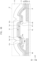
- FIG. 8B is an enlarged schematic sectional view illustrating a portion of the display panel DP (refer to FIG. 1A ) according to an embodiment.
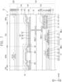
- FIG. 8B is a schematic sectional view of region AA' illustrated in FIG. 7 according to an embodiment.
- valleys VP1a and VP2a overlapping the non-emissive region NPXA may be defined in the pixel defining layer PDL.
- Each of the valleys VP1a and VP2a may be defined by a valley bottom surface VBSa and a valley tapered surface VTSa.
- the valley bottom surface VBSa and the valley tapered surface VTSa may be connected to each other.
- the taper angle AG2 at which the valley tapered surface VTSa is inclined with respect to a plane aligned with the valley bottom surface VBSa may have a certain angle.
- the certain angle may range from about 70 degrees to about 80 degrees.
- the thickness of the intermediate layer CEL and the thickness of the second electrode CE may be decreased by the valleys VP1a and VP2a.
- a portion of the intermediate layer CEL may be cut off at portions overlapping the valleys VP1a and VP2a.
- the resistances of the intermediate layer CEL and the second electrode CE may be increased in the portions overlapping the valleys VP1a and VP2a. Accordingly, a current may be prevented from being leaked into the portions where the valleys VP1a and VP2a are formed.
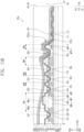
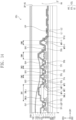
- FIG. 9 is an image of a portion of the display panel DP (refer to FIG. 1A ) according to an embodiment.
- the image illustrated in FIG. 9 is an image of the portion of the pixel defining layer PDL where the valley bottom surface VBS is defined.
- the pixel defining layer PDL may include a black coloring agent.
- the black coloring agent may include carbon black, metal such as chromium, or oxide thereof.
- an uneven surface may be formed by the black coloring agent.
- FIG. 10 is an enlarged schematic plan view illustrating a portion of the display panel DP (refer to FIG. 1A ) according to an embodiment.
- FIG. 10 is an enlarged schematic sectional view illustrating region BB' illustrated in FIG. 1A .
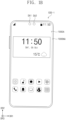
- a hole HA may be defined in the display panel DP.
- the hole HA may be defined by removing a portion of the display panel DP.
- the active region 1000A of the display panel DP may surround the hole HA.
- the hole HA may overlap or correspond to the sensor region SA1.
- the hole HA is illustrated in a circular shape in the embodiment, the hole HA may have various shapes, such as a polygonal shape, an oval shape, a shape having at least one curved side, or an irregular shape, and is not limited to any one embodiment.
- the hole HA may be formed after both the display layer 100 (refer to FIG. 3 ) and the sensor layer 200 (refer to FIG. 3 ) are formed. In another example, the hole HA may be formed after the display layer 100 is formed.
- a process of forming the hole HA may include a process of applying a laser to the rear surface of the base layer 110 (refer to FIG. 3 ) and a process of providing an etchant toward the rear surface of the base layer 110.
- the process of applying the laser may be a process of sketching, on the base layer 110, a region to be removed.
- the etchant may be provided in a direction from the rear surface to the upper surface of the base layer 110 along the third direction DR3.
- the display panel DP may further include dams DM1, DM2, DM3, DM4, and DM5 adjacent to the hole HA.
- the dams DM1, DM2, DM3, DM4, and DM5 may control a flow of monomer during a process of forming the second encapsulation layer 142 or to protect the element layer 130 during a process of forming the hole HA.
- the five dams DM1, DM2, DM3, DM4, and DM5 are illustrated as an example in FIG. 10 , embodiments are not limited thereto. Some of the five dams DM1, DM2, DM3, DM4, and DM5 may be omitted, and more dams may be disposed.
- FIG. 11A is a schematic sectional view of the display panel DP according to an embodiment.
- FIG. 11A may be a schematic sectional view taken along line II-II' of FIG. 10 .
- the display panel DP may include a sidewall DP-HS that defines the hole HA.
- the display panel DP may include the dams DM1, DM2, DM3, DM4, and DM5 and inorganic dams IOP adjacent to the hole HA.
- the five dams DM1, DM2, DM3, DM4, and DM5 and three inorganic dams IOP are illustrated as an example in FIG. 11A , embodiments are not limited thereto. Some of the five dams DM1, DM2, DM3, DM4, and DM5 and the three inorganic dams IOP may be omitted, and more dams may be disposed.
- the dams DM1, DM2, DM3, DM4, and DM5 may include the first dam DM1, the second dam DM2, the third dam DM3, the fourth dam DM4, and the fifth dam DM5.
- the first to fourth dams DM1, DM2, DM3, and DM4 may control the flow of the monomer during the process of forming the second encapsulation layer 142.
- the fifth dam DM5 and the inorganic dams IOP may prevent propagation of a crack progressing from the sidewall DP-HS. Accordingly, the fifth dam DM5 may be referred to as the crack dam.
- the inorganic dams IOP may be referred to as the inorganic patterns.
- each of the first dam DM1 and the fourth dam DM4 may include a first conductive layer MP1, the second insulating layer 20, a second conductive layer MP2, the third insulating layer 30, a third conductive layer MP3, a first dam layer DMI,a, a fourth conductive layer MP4, a second dam layer DMI,b, and a third dam layer DMI,c.
- the first conductive layer MP1, the first gate electrode E13 of the first thin film transistor T1, the second gate electrode E23 of the second thin film transistor T2, the first counter electrode Cs1 of the transfer capacitor Cst, and the first hold counter electrode Ch1 of the hold capacitor Chold may be disposed on the same layer.
- the first conductive layer MP1, the first gate electrode E13 of the first thin film transistor T1, the second gate electrode E23 of the second thin film transistor T2, the first counter electrode Cs1 of the transfer capacitor Cst, and the first hold counter electrode Ch1 of the hold capacitor Chold may include the same material.
- the second conductive layer MP2, the second counter electrode Cs2 of the transfer capacitor Cst and the second hold counter electrode Ch2 of the hold capacitor Chold may be disposed on the same layer.
- the second conductive layer MP2, the second counter electrode Cs2 of the transfer capacitor Cst and the second hold counter electrode Ch2 of the hold capacitor Chold may include the same material.
- the third conductive layer MP3 and the first connecting electrode CNE10 may be disposed on the same layer and may include the same material.
- the fourth conductive layer MP4, and the second connecting electrode CNE20 may include the same material as the second connecting electrode CNE20 may be disposed on the same layer.
- the first dam layer DMI,a and the fourth insulating layer 40 may include the same material.
- the first dam layer DMI,a may be a portion of the fourth insulating layer 40.
- the second dam layer DMLb and the fifth insulating layer 50 may include the same material.
- the second dam layer DMLb may be a portion of the fifth insulating layer 50.
- the third dam layer DMLc and the pixel defining layer PDL may be disposed on the same layer and may include the same material.
- the second dam DM2 and the third dam DM3 may have a smaller height or thickness than the first and fourth dams DM1 and DM4.
- each of the second dam DM2 and the third dam DM3 may include a first conductive layer MP1, the second insulating layer 20, a second conductive layer MP2, the third insulating layer 30, a third conductive layer MP3, a first dam layer DMLa, a fourth conductive layer MP4, and a second dam layer DMLb.
- the fourth conductive layer MP4 of each of the first to fourth dams DM1, DM2, DM3, and DM4 may be brought into contact with the third conductive layer MP3.
- the continuity of the fourth insulating layer 40 may be broken by the third conductive layer MP3 and the fourth conductive layer MP4 brought into contact with each other. Accordingly, a path along which the etchant is able to infiltrate in the case that the hole HA is processed may be shielded by the first to fourth dams DM1, DM2, DM3, and DM4.
- the fifth dam DM5 may be disposed closest to the hole HA.
- the fifth dam DM5 may include the second insulating layer 20, the third insulating layer 30, a third conductive layer MP3-1, a first dam layer DMI,a, a fourth conductive layer MP4-1, and a second dam layer DMLb.
- the fourth conductive layer MP4-1 of the fifth dam DM5 may be brought into contact with the third conductive layer MP3-1.
- the continuity of the fourth insulating layer 40 may be broken (or discontinued) by the third conductive layer MP3-1 and the fourth conductive layer MP4-1 brought into contact with each other. Accordingly, a path along which the etchant is able to infiltrate in the case that the hole HA is processed may be additionally shielded by the fifth dam DM5. Accordingly, the reliability of the display panel DP may be further improved.
- each of the inorganic dams IOP may include a first dam layer IL1 and a second dam layer IL2.
- the first dam layer IL1 and the second insulating layer 20 may include the same material and may be formed by the same process.
- the second dam layer IL2 and the third insulating layer 30 may include the same material and may be formed by the same process.
- the width of the first dam layer IL1 may be greater than the width of the second dam layer IL2. Accordingly, each of the inorganic dams IOP may have a step shape.
- First to fifth grooves GV1, GV2, GV3, GV4, and GV5 may be defined adjacent to the first to fifth dams DM1, DM2, DM3, DM4, and DM5.
- the first groove GV1 and the second groove GV2 may be spaced apart from each other with the first dam DM1 between first groove GV1 and the second groove GV2.
- the second groove GV2 and the third groove GV3 may be spaced apart from each other with the second dam DM2 between the second groove GV2 and the third groove GV3.
- the third groove GV3 and the fourth groove GV4 may be spaced apart from each other with the third dam DM3 between the third groove GV3 and the fourth groove GV4.
- the fourth groove GV4 and the fifth groove GV5 may be spaced apart from each other with the fourth dam DM4 between the fourth groove GV4 and the fifth groove GV5.
- the first to fifth grooves GV1, GV2, GV3, GV4, and GV5 may be formed by the same process as the process of forming the valleys VP1, VP2, and VP3 (refer to FIG. 6 ). Accordingly, an additional process for forming the first to fifth grooves GV1, GV2, GV3, GV4, and GV5 may be omitted. For example, the number of masks used during the process of forming the display panel DP may be decreased, and the manufacturing cost of the display panel DP may be reduced.
- the first to fifth grooves GV1, GV2, GV3, GV4, and GV5 may be formed by the same process as the valleys VP1, VP2, and VP3. Accordingly, the depths of the first to fifth grooves GV1, GV2, GV3, GV4, and GV5 may be determined according to the depths of the valleys VP1, VP2, and VP3. For example, the bottom surfaces of the first to fifth grooves GV1, GV2, GV3, GV4, and GV5 may be defined in the fourth insulating layer 40.
- each of the first to fourth dams DM1, DM2, DM3, and DM4 may have a double wing structure including tip portions protruding in opposite directions. As many as possible of the tip portions may be provided, and thus a common layer CCL may be stably disconnected. Accordingly, the reliability of the display panel DP may be further improved.
- each of the first to fourth dams DM1, DM2, DM3, and DM4 may be disposed between the first to fifth grooves GV1, GV2, GV3, GV4, and GV5.
- the number of tip portions may be twice or more the number of first to fourth dams DM1, DM2, DM3, and DM4. Accordingly, the number of tip portions may be 8 or more.
- the display panel DP may include tip portions TP1, TP2, TP3, TP4, TP5, TP6, TP7, TP8, TP9, and TP10.
- the first to fifth grooves GV1, GV2, GV3, GV4, and GV5 may be provided to form at least some of the tip portions TP1, TP2, TP3, TP4, TP5, TP6, TP7, TP8, TP9, and TP10.
- the shapes of the tip portions TP1, TP2, TP3, TP4, TP5, TP6, TP7, TP8, TP9, and TP10 in plan view may be similar to the shapes of the first to fifth grooves GV1, GV2, GV3, GV4, and GV5 in plan view.
- Each of the tip portions TP1, TP2, TP3, TP4, TP5, TP6, TP7, TP8, TP9, and TP10 may have a shape surrounding the hole HA (refer to FIG. 10 ).
- a third tip portion TP3 may have a shape surrounding the hole HA
- a second tip portion TP2 may have a shape surrounding the third tip portion TP3.
- the tip portions TP1, TP2, TP3, TP4, TP5, TP6, TP7, TP8, TP9, and TP10 may disconnect the common layer CCL formed with an open mask.
- the common layer CCL may include the first functional layer HFL, the second functional layer EFL, and the second electrode CE.
- Portions of the common layer CCL disconnected by the tip portions TP1, TP2, TP3, TP4, TP5, TP6, TP7, TP8, TP9, and TP10, for example, disconnected layers GCP may overlap the first to fifth grooves GV1, GV2, GV3, GV4, and GV5.
- the first tip portion TP1 and the second tip portion TP2 may overlap the first groove GV1.
- the third tip portion TP3 and the fourth tip portion TP4 may overlap the second groove GV2.
- the fifth tip portion TP5 and the sixth tip portion TP6 may overlap the third groove GV3.
- the seventh tip portion TP7 and the eighth tip portion TP8 may overlap the fourth groove GV4.
- the ninth tip portion TP9 may overlap the fifth groove GV5.
- the tenth tip portion TP10 may protrude from the fifth dam DM5 in a direction toward the hole HA.
- the first encapsulation layer 141 may cover all of the first to fifth grooves GV1, GV2, GV3, GV4, and GV5.
- the second encapsulation layer 142 may be disposed on the first encapsulation layer 141 and may overlap at least some of the first to fifth grooves GV1, GV2, GV3, GV4, and GV5.
- the second encapsulation layer 142 may overlap the first to fourth grooves GV1, GV2, GV3, and GV4.
- the third encapsulation layer 143 may be disposed on the second encapsulation layer 142 and may cover all of the first to fifth grooves GV1, GV2, GV3, GV4, and GV5.
- the first sensor conductive layer 220 of the sensor layer 200 may include a first clad pattern 220cp
- the second sensor conductive layer 240 of the sensor layer 200 may include a second clad pattern 240cp.
- Each of the first clad pattern 220cp and the second clad pattern 240cp may overlap the remaining groove not overlapping the second encapsulation layer 142, for example, the fifth groove GV5.
- each of the first clad pattern 220cp and the second clad pattern 240cp may overlap the fifth dam DM5 (referred to as the crack dam) and the tenth tip portion TP10 protruding from the fifth dam DM5 toward the hole HA.
- the flexure of the third encapsulation layer 143 may be increased by the fifth groove GV5 in which the second encapsulation layer 142 is not disposed.
- the film quality of the third encapsulation layer 143 may be deteriorated due to the flexure, and therefore the third encapsulation layer 143 may be cracked.
- the third encapsulation layer 143 may be oxidized even though the third encapsulation layer 143 includes silicon nitride.
- the first and second clad patterns 220cp and 240cp may be disposed in a region overlapping the fifth groove GV5. Accordingly, even though the third encapsulation layer 143 is cracked or oxidized, moisture and oxygen may be blocked by the first and second clad patterns 220cp and 240cp. Accordingly, the product reliability of the display panel DP may be improved.
- FIG. 11B is a schematic sectional view of a display panel DPa according to an embodiment.
- components identical to the components described with reference to FIG. 11A will be assigned with identical reference numerals, and descriptions thereabout will be omitted for descriptive convenience.
- a first sensor conductive layer 220 of a sensor layer 200 may include a first clad pattern 220cp.
- the first clad pattern 220cp may overlap the remaining groove not overlapping a second encapsulation layer 142, for example, a fifth groove GV5.
- the first clad pattern 220cp may overlap a fifth dam DM5 (referred to as the crack dam) and a tenth tip portion TP10 protruding from the fifth dam DM5 toward a hole HA. Accordingly, even though a third encapsulation layer 143 is cracked or oxidized, moisture and oxygen may be blocked by the first clad pattern 220cp. Accordingly, the product reliability of the display panel DPa may be improved.
- FIG. 11C is a schematic sectional view of a display panel DPb according to an embodiment.
- components identical to the components described with reference to FIG. 11A will be assigned with identical reference numerals, and descriptions thereabout will be omitted for descriptive convenience.
- a second sensor conductive layer 240 of a sensor layer 200 may include a second clad pattern 240cp.
- the second clad pattern 240cp may overlap the remaining groove not overlapping a second encapsulation layer 142, for example, a fifth groove GV5.
- the second clad pattern 240cp may overlap a fifth dam DM5 (referred to as the crack dam) and a tenth tip portion TP10 protruding from the fifth dam DM5 toward a hole HA. Accordingly, even though a third encapsulation layer 143 is cracked or oxidized, moisture and oxygen may be blocked by the second clad pattern 240cp. Accordingly, the product reliability of the display panel DPb may be improved.
- FIG. 12A is a schematic sectional view of the display panel DP (refer to FIG. 11A ) according to an embodiment.
- FIG. 12A is an enlarged schematic sectional view illustrating region CC' illustrated in FIG. 11A .
- FIG. 12A is an enlarged schematic sectional view illustrating the region where the second groove GV2 is defined. The following description may be identically applied to the first groove GV1, the third groove GV3, and the fourth groove GV4.
- each of the third conductive layer MP3 and the fourth conductive layer MP4 may have a multi-layer structure.
- each of the third conductive layer MP3 and the fourth conductive layer MP4 may have a three-layer structure of titanium (Ti)/aluminium (Al)/titanium (Ti).
- the third conductive layer MP3 may include a first sub-conductive layer MP3a, a second sub-conductive layer MP3b, and a third sub-conductive layer MP3c.
- the fourth conductive layer MP4 may include a first sub-conductive layer MP4a, a second sub-conductive layer MP4b, and a third sub-conductive layer MP4c.
- the first sub-conductive layer MP3a, the third sub-conductive layer MP3c, the first sub-conductive layer MP4a, and the third sub-conductive layer MP4c may include titanium, and the second sub-conductive layer MP3b and the second sub-conductive layer MP4b may include aluminium.
- embodiments are not limited thereto.
- a first side surface S 1 of the first sub-conductive layer MP4a, a second side surface S2 of the second sub-conductive layer MP4b, and a third side surface S3 of the third sub-conductive layer MP4c that define a side surface SS of each of the third tip portion TP3 and the fourth tip portion TP4 may be aligned with one another.
- the shape of the first to third side surfaces S1, S2, and S3 may vary according to components of an etchant used in a process of forming the first electrode AE, e.g., a process of making the first electrode AE subject to patterning or the materials of the first sub-conductive layer MP4a, the second sub-conductive layer MP4b, and the third sub-conductive layer MP4c.
- the etchant may include a non-phosphoric acid-based etching composition.
- the first to third side surfaces S1, S2, and S3 may have an aligned shape.
- a bottom surface GV-B of the second groove GV2 and side surfaces GV-S connected to the bottom surface GV-B may be defined by a single insulating layer, for example, the fourth insulating layer 40.
- the fourth insulating layer 40 may be an organic insulating layer.
- the second groove GV2 and the valleys VP1 and VP2 may be formed by the same process. Accordingly, the shape of the second groove GV2 may be similar to the shapes of the valleys VP1 and VP2.
- the side surfaces GV-S of the second groove GV2 may include a curved surface GV-C extending from the bottom surface GV-B and a tapered surface GV-T extending from the curved surface GV-C.
- the radius of curvature of the curved surface GV-C may range from about 100 nm to about 230 nm, but embodiments are not limited thereto.
- the taper angle AG1 at which the valley tapered surface VTS is inclined with respect to the plane aligned with the valley bottom surface VBS may be substantially the same as the angle AG3 of the tapered surface GV-T with respect to a plane aligned with the bottom surface GV-B.
- the angle AG3 of the tapered surface GV-T may range from about 70 degrees to about 80 degrees, but embodiments are not limited thereto.
- the depths of the first to fifth grooves GV1, GV2, GV3, GV4, and GV5 may be determined according to the depths VP-D of the valleys VP1 and VP2.
- the depths VP-D of the valleys VP1 and VP2 may be substantially the same as the height TP-H of the fourth tip portion TP4, which is measured from the bottom surface GV-B of the second groove GV2 to a bottom surface of the fourth tip portion TP4.
- a difference between the width TP-W and the height TP-H of the fourth tip portion TP4 may be less than about 0.15 micrometers and, for example, may be about 0.05 micrometers.
- the width TP-W of the fourth tip portion TP4 may correspond to the width of the exposed lower surface of the fourth conductive layer MP4.
- the width TP-W of the fourth tip portion TP4 may be about 0.4 micrometers or less
- the height TP-H of the fourth tip portion TP4 may be about 0.45 micrometers or less.
- the width TP-W of the fourth tip portion TP4 may be about 0.4 micrometers
- the height TP-H of the fourth tip portion TP4 may be about 0.45 micrometers.
- the first encapsulation layer 141 may be disposed on the common layer CCL.
- the first encapsulation layer 141 may be formed by a deposition process, for example, a chemical vapor deposition (CVD) process.
- the first encapsulation layer 141 may be formed to correspond to the shapes of the third tip portion TP3 and the fourth tip portion TP4.
- the thickness 141-t2 of a portion of the first encapsulation layer 141 disposed under the third tip portion TP3 and the fourth tip portion TP4 may be less than the thickness 141-t1 of a portion of the first encapsulation layer 141 disposed on the third tip portion TP3 and the fourth tip portion TP4.
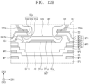
- FIG. 12B is a schematic sectional view of the display panel DP (refer to FIG. 11A ) according to an embodiment.
- the fourth conductive layer MP4 may have a multi-layer structure.
- the fourth conductive layer MP4 may include a first sub-conductive layer MP4a, a second sub-conductive layer MP4b, and a third sub-conductive layer MP4c.
- a first side surface S1a of the first sub-conductive layer MP4a, a second side surface S2a of the second sub-conductive layer MP4b, and a third side surface S3a of the third sub-conductive layer MP4c that define a side surface SSa of each of a third tip portion TP3a and a fourth tip portion TP4a may not be aligned with one another.
- the second side surface S2a may have a shape recessed with respect to (or from) the first side surface S1a and the third side surface S3a.
- the shapes of the first to third side surfaces S1a, S2a, and S3a may vary according to components of an etchant used in a process of forming the first electrode AE or the materials of the first sub-conductive layer MP4a, the second sub-conductive layer MP4b, and the third sub-conductive layer MP4c.
- the etchant may include a phosphoric acid-based etching composition
- the first sub-conductive layer MP4a and the third sub-conductive layer MP4c may include titanium
- the second sub-conductive layer MP4b may include aluminium.
- a bottom surface GV-B of the second groove GV2 and a side surface GV-Sa connected to the bottom surface GV-B may be defined (or formed) by an insulating layer (or single layer), for example, the fourth insulating layer 40.
- the fourth insulating layer 40 may be an organic insulating layer.
- the second groove GV2 and the valleys VP1a and VP2a may be formed by the same process. Accordingly, the shape of the second groove GV2 may be similar to the shapes of the valleys VP1a and VP2a.
- the taper angle AG2 at which the valley tapered surface VTSa is inclined with respect to the plane aligned with the valley bottom surface VBS may be substantially the same as the angle AG4 of the side surface GV-Sa with respect to a plane aligned with the bottom surface GV-B.
- FIG. 12C is a schematic sectional view of the display panel DP (refer to FIG. 11A ) according to an embodiment.
- the fourth conductive layer MP4 may have a multi-layer structure.
- the fourth conductive layer MP4 may include a first sub-conductive layer MP4a, a second sub-conductive layer MP4b, and a third sub-conductive layer MP4c.
- a first side surface S1b of the first sub-conductive layer MP4a, a second side surface S2b of the second sub-conductive layer MP4b, and a third side surface S3b of the third sub-conductive layer MP4c that define a side surface SSb of each of a third tip portion TP3b and a fourth tip portion TP4b may not be aligned with one another.
- the second side surface S2b may have a shape protruding with respect to (or from) the first side surface S1b and the third side surface S3b.
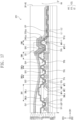
- FIG. 13 is an image of a portion of the display panel DP (refer to FIG. 1A ) according to an embodiment.
- the thickness 141-t2 of a portion of the first encapsulation layer 141 disposed under the third tip portion TP3 and the fourth tip portion TP4 may be less than the thickness 141-11 of a portion of the first encapsulation layer 141 disposed on the third tip portion TP3 and the fourth tip portion TP4. Accordingly, a certain space 141sp may be defined in a region under each of the third tip portion TP3 and the fourth tip portion TP4 by the first encapsulation layer 141. The space 141sp may be filled with the material of the second encapsulation layer 142.
- FIG. 14 is a schematic sectional view of a display panel DPc according to an embodiment.
- components identical to the components described with reference to FIG. 11A will be assigned with identical reference numerals, and descriptions thereabout will be omitted for descriptive convenience.
- the display panel DPc may further include a cover layer YOC.
- the cover layer YOC may be disposed on the third encapsulation layer 143.
- the cover layer YOC may be a layer provided to improve a step of a region adjacent to a hole HA.
- the cover layer YOC may include an organic material, but embodiments are not limited thereto.
- the cover layer YOC may be referred to as the compensation layer, the step compensation layer, the planarization layer, or the partial planarization layer.
- a sensor layer 200 may be disposed on the cover layer YOC.
- the cover layer YOC may be disposed in the region adjacent to the hole HA to provide a flat base surface. Accordingly, the sensor layer 200 may be readily formed on the flat surface.
- FIG. 15 is a schematic sectional view of a display panel DPd according to an embodiment.
- components identical to the components described with reference to FIG. 11A will be assigned with identical reference numerals, and descriptions thereabout will be omitted for descriptive convenience.
- the display panel DPd may include dams DM1, DM2, DM3, DM4, and DM5a and inorganic dams IOP adjacent to a hole HA.
- the dams DM1, DM2, DM3, DM4, and DM5a may include the first dam DM1, the second dam DM2, the third dam DM3, the fourth dam DM4, and the fifth dam DM5a.
- the fifth dam DM5a may be disposed closest to the hole HA.
- the fifth dam DM5a may include a second insulating layer 20, a third insulating layer 30, a third conductive layer MP3-2, a first dam layer DMLa, a fourth conductive layer MP4-2, and a second dam layer DMI,b.
- the fourth conductive layer MP4-2 of the fifth dam DM5a may not be brought into contact with the third conductive layer MP3-2. Accordingly, the continuity of the fourth insulating layer 40 may not be broken in the region where the fifth dam DM5a is disposed.
- a tenth tip portion TP10 protruding toward the hole HA may be disposed in the fifth dam DM5a. The tenth tip portion TP10 may prevent a crack progressing from a sidewall DP-HS from propagating into the display panel DPd. Accordingly, the fifth dam DM5 may be referred to as the crack dam.
- FIG. 16 is a schematic sectional view of a display panel DPe according to an embodiment.
- components identical to the components described with reference to FIG. 11A will be assigned with identical reference numerals, and descriptions thereabout will be omitted for descriptive convenience.
- the display panel DPe may include dams DM1, DM2, DM3, DM4, and DM5 adjacent to a hole HA.
- the display panel DPe may not include the inorganic dams IOP.
- the inorganic dams IOP are omitted, the area of a non-display region around the hole HA may be reduced.
- a process may be simplified.
- FIG. 17 is a schematic sectional view of a display panel DPf according to an embodiment.
- components identical to the components described with reference to FIG. 11A will be assigned with identical reference numerals, and descriptions thereabout will be omitted for descriptive convenience.
- the display panel DPf may include dams DM1, DM2a, DM3a, DM4, and DM5 and inorganic dams IOP adjacent to a hole HA.
- the dams DM1, DM2a, DM3a, DM4, and DM5 may include the first dam DM1, the second dam DM2a, the third dam DM3a, the fourth dam DM4, and the fifth dam DM5.
- Each of the first to fourth dams DM1, DM2a, DM3a, and DM4 may be disposed between grooves.
- the first dam DM1 and the fourth dam DM4 may have the greatest height (or thickness).
- the second dam DM2a and the third dam DM3a may have a smaller height or thickness than the first and fourth dams DM1 and DM4.
- each of the first dam DM1 and the fourth dam DM4 may have a double wing structure including tip portions protruding in opposite directions.
- the second dam DM2a and the third dam DM3a may have a single wing structure including a tip portion protruding in one direction.
- the display panel DPf may not include the fifth tip portion TP5 and the seventh tip portion TP7.
- one of the second dam DM2a and the third dam DM3a may have a double wing structure including tip portions protruding in opposite directions, and the other one of the second dam DM2a and the third dam DM3a may have a single wing structure.
- FIG. 18 is an enlarged schematic sectional view illustrating a portion of a display panel DPf (refer to FIG. 17 ) according to an embodiment.
- FIG. 18 is an enlarged schematic sectional view illustrating region DD' illustrated in FIG. 17 .
- disconnected layers GCPa may be disposed in a fifth groove GV5.
- the disconnected layers GCPa may be disconnected by a ninth tip portion TP9 and may extend above the fifth dam DM5.
- a first encapsulation layer 141 may cover the fifth groove GV5.
- a certain space 141spa may be defined under the ninth tip portion TP9.
- the space 141spa may have an open structure that is not completely closed by the first encapsulation layer 141.
- a monomer may or may not be disposed in the region where the fifth groove GV5 is defined. Accordingly, the space 141spa may or may not be filled with the material of the second encapsulation layer 142.
- FIG. 18 illustrates an example that the space 141spa is filled with a material of a third encapsulation layer 143
- the space 141spa may have a structure completely closed by the first encapsulation layer 141 and the third encapsulation layer 143.
- the space 141spa may contain a gas used during a process of forming the first encapsulation layer 141, or may be in a vacuum state.
- first and second clad patterns 220cp and 240cp may be disposed in a region overlapping the fifth groove GV5. Accordingly, even though the third encapsulation layer 143 is cracked or oxidized, moisture and oxygen may be blocked by the first and second clad patterns 220cp and 240cp. Accordingly, the product reliability of the display panel DPf may be improved.
- FIG. 19 is an enlarged schematic sectional view illustrating a portion of a display panel DPf (refer to FIG. 17 ) according to an embodiment.
- FIG. 19 is an enlarged schematic sectional view illustrating region DD' illustrated in FIG. 17 .
- components identical to the components described with reference to FIG. 18 will be assigned with identical reference numerals, and descriptions thereabout will be omitted for descriptive convenience.
- a first encapsulation layer 141 may cover a fifth groove GV5.
- a certain space 141spb may be defined under the ninth tip portion TP9.
- the space 141spb may have a structure completely closed by the first encapsulation layer 141.
- another material for example, a material of a second encapsulation layer 142 or a material of a third encapsulation layer 143 may not be disposed in the space 141spb.
- the space 141spb may contain a gas used during a process of forming the first encapsulation layer 141, or may be in a vacuum state.
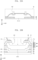
- FIGS. 20A, 20B , 21A, 21B , 22A, 22B , 23A, 23B , 24A, and 24B are schematic sectional views illustrating some steps of a display panel manufacturing process according to an embodiment.
- FIGS. 20A , 21A , 22A , 23A , and 24A are sectional views illustrating a process of forming valleys VP in a preliminary pixel defining layer PDL-bf (e.g., in an upper surface of the preliminary pixel defining layer PDL-bf).
- FIGS. 20B , 21B , 22B , 23B , and 24B are schematic sectional views illustrating a process of forming a second groove GV2 on a preliminary insulating layer 40-bf (e.g., in an upper surface of the preliminary insulating layer 40-bf).
- the following description may be identically applied to the first groove GV1, the third groove GV3, and the fourth groove GV4 described above.
- FIGS. 20A and 20B a region corresponding to region AA' and a region corresponding to region CC' that are placed in the same process are illustrated.
- a first electrode AE may be formed on a fifth insulating layer 50
- the preliminary pixel defining layer PDL-bf may be formed on the first electrode AE.
- a third tip portion TP3 and a fourth tip portion TP4 that are not covered by the fifth insulating layer 50 are defined.
- a portion of the preliminary insulating layer 40-bf is exposed between the third tip portion TP3 and the fourth tip portion TP4.
- the preliminary insulating layer 40-bf is a layer corresponding to the fourth insulating layer 40 (refer to FIG. 11A ).
- a mask layer MP may cover the first electrode AE, the preliminary pixel defining layer PDL-bf, the fifth insulating layer 50, the third tip portion TP3, and the fourth tip portion TP4.
- the mask layer MP may have a first opening MP-OP1 and a second opening MP-OP2 defined therein.
- the first opening MP-OP1 may overlap the preliminary pixel defining layer PDL-bf
- the second opening MP-OP2 may overlap a portion of the preliminary insulating layer 40-bf, a portion of the third tip portion TP3, and a portion of the fourth tip portion TP4.
- the mask layer MP may include indium gallium zinc oxide (IGZO), but embodiments are not limited thereto.
- a sidewall defining the second opening MP-OP2 of the mask layer MP may be spaced apart from an end portion of the third tip portion TP3 and an end portion of the fourth tip portion TP4.
- the upper surface of the third tip portion TP3 and the upper surface of the fourth tip portion TP4 may be exposed by at least 0.5 micrometers or more.
- first etching EC1 may be simultaneously performed on the preliminary pixel defining layer PDL-bf and the preliminary insulating layer 40-bf.
- the first etching EC1 may be dry etching and may be anisotropic etching having specific orientation. Grooves having substantially the same depth may be formed in the preliminary pixel defining layer PDL-bf and the preliminary insulating layer 40-bf (e.g., in upper surfaces thereof) by the first etching EC1.
- second etching EC2 may be simultaneously performed on the preliminary pixel defining layer PDL-bf and the preliminary insulating layer 40-bf.
- the second etching EC2 may be dry etching and may be isotropic etching. Spaces formed by the first etching EC1 and the second etching EC2 may have an undercut shape with respect to the mask layer MP or the third and fourth tip portions TP3 and TP4.
- a pixel defining layer PDL having the valleys VP defined therein and a fourth insulating layer 40 having the second groove GV2 defined therein may be formed.
- the valleys VP and the second groove GV2 formed by the same process may have similar shapes.
- the depths VP-D of the valleys VP may be substantially the same as the depth GV-D of the second groove GV2 defined by (or formed in) the fourth insulating layer 40.
- the pixel defining layer PDL may include a black coloring agent.
- the black coloring agent may include carbon black, metal such as chromium, or oxide thereof.
- an uneven surface may be formed by the black coloring agent.
- the fourth insulating layer 40 may not include the black coloring agent. Accordingly, the roughness of the bottom surface of the second groove GV2 may be lower than the roughness of the bottom surface of each of the valleys VP.
- the bottom surface of the second groove GV2 may be smoother than the bottom surfaces of the valleys VP.
- the first to fifth grooves GV1, GV2, GV3, GV4, and GV5 may be formed by the same process as the process of forming the valleys VP. Accordingly, an additional process for forming the first to fifth grooves GV1, GV2, GV3, GV4, and GV5 may be omitted. For example, the number of masks used during the process of forming the display panel DP may be decreased, and the manufacturing cost of the display panel DP may be reduced.
- FIGS. 25A, 25B , 26A, 26B , 27A, 27B , 28A, and 28B are schematic sectional views illustrating some steps of a display panel manufacturing process according to an embodiment.
- FIGS. 25A , 26A , 27A , and 28A are schematic sectional views illustrating a process of forming valleys VP in a preliminary pixel defining layer PDL-bfa (e.g., in an upper surface of the preliminary pixel defining layer PDL-bfa).
- FIGS. 25B , 26B , 27B , and 28B are schematic sectional views illustrating a process of forming a second groove GV2a in a preliminary insulating layer 40-bf (e.g., in an upper surface of the preliminary insulating layer 40-bf).
- the following description may be identically applied to the first groove GV1, the third groove GV3, and the fourth groove GV4 described above.
- a first electrode AE may be formed on a fifth insulating layer 50, and the preliminary pixel defining layer PDL-bfa having an opening OP formed therein may be formed on the first electrode AE.
- the preliminary pixel defining layer PDL-bfa may include protruding portions PDLpt. The protruding portions PDLpt may overlap the positions in which the valleys VP, which will be described below, are to be formed.
- a third tip portion TP3 and a fourth tip portion TP4 that are not covered by the fifth insulating layer 50 are defined.
- a portion of the preliminary insulating layer 40-bf is exposed between the third tip portion TP3 and the fourth tip portion TP4.
- the preliminary insulating layer 40-bf is a layer corresponding to the fourth insulating layer 40 (refer to FIG. 11A ).
- a mask layer MP may cover the first electrode AE, the preliminary pixel defining layer PDL-bfa, the fifth insulating layer 50, the third tip portion TP3, and the fourth tip portion TP4.
- the mask layer MP may have a first opening MP-OP1 and a second opening MP-OP2 defined therein.
- the first opening MP-OP1 may overlap the preliminary pixel defining layer PDL-bfa
- the second opening MP-OP2 may overlap a portion of the preliminary insulating layer 40-bf, a portion of the third tip portion TP3, and a portion of the fourth tip portion TP4.
- the mask layer MP may include indium gallium zinc oxide (IGZO), but embodiments are not limited thereto.
- first etching EC1a may be simultaneously performed on the preliminary pixel defining layer PDL-bfa and the preliminary insulating layer 40-bf.
- the first etching EC1a may be dry etching and may be anisotropic etching having specific orientation.
- the preliminary pixel defining layer PDL-bfa may include the protruding portions PDLpt.
- the depth of grooves (i.e., valleys) formed in the preliminary pixel defining layer PDL-bfa may be shallower than the depth of a groove formed in the preliminary insulating layer 40-bf.
- second etching EC2 may be simultaneously performed on the preliminary pixel defining layer PDL-bfa and the preliminary insulating layer 40-bf.
- the second etching EC2 may be dry etching and may be isotropic etching. Spaces formed by the first etching EC1a and the second etching EC2 may have an undercut shape with respect to the mask layer MP or the third and fourth tip portions TP3 and TP4.
- a pixel defining layer PDL having the valleys VP defined therein and a fourth insulating layer 40a having the second groove GV2a defined therein may be formed.
- the valleys VP and the second groove GV2a formed by the same process may have similar shapes. Since the preliminary pixel defining layer PDL-bfa includes the protruding portions PDLpt before the process, the depths VP-D of the valleys VP may be shallower than the depth GV-Da of the second groove GV2a defined by (or formed in) the fourth insulating layer 40a.
- the grooves and the valleys formed by the same process may be defined in the display panel. Accordingly, an additional process for forming the grooves may be omitted. For example, the number of masks used in the process of forming the display panel may be decreased, and the manufacturing cost of the display panel may be reduced.
- the path along which the etchant is able to infiltrate in the case that the hole of the display panel is processed may be shielded by the dams. Furthermore, the path may be additionally shielded by the crack dam disposed closest to the hole.
- each of the dams defined between the grooves may include the tip portions protruding in the opposite directions. Accordingly, even though the depths of the grooves are decreased, as many as possible of the tip portions may be provided, and thus the common layer may be stably disconnected. Thus, the reliability of the display panel may be further improved.
- the region overlapping the groove not covered by the organic encapsulation layer among the grooves may be covered by at least one clad pattern. Accordingly, even though the inorganic encapsulation layer is cracked by the flexure of the groove or oxidized, moisture and oxygen may be blocked by the clad pattern. Thus, the product reliability of the display panel may be improved.
Landscapes
- Engineering & Computer Science (AREA)
- Microelectronics & Electronic Packaging (AREA)
- Physics & Mathematics (AREA)
- General Engineering & Computer Science (AREA)
- Theoretical Computer Science (AREA)
- Chemical & Material Sciences (AREA)
- Inorganic Chemistry (AREA)
- Human Computer Interaction (AREA)
- General Physics & Mathematics (AREA)
- Optics & Photonics (AREA)
- Manufacturing & Machinery (AREA)
- Geometry (AREA)
- Life Sciences & Earth Sciences (AREA)
- Sustainable Development (AREA)
- Electroluminescent Light Sources (AREA)
- Devices For Indicating Variable Information By Combining Individual Elements (AREA)
Applications Claiming Priority (1)
| Application Number | Priority Date | Filing Date | Title |
|---|---|---|---|
| KR1020230109166A KR20250028584A (ko) | 2023-08-21 | 2023-08-21 | 표시 패널 |
Publications (1)
| Publication Number | Publication Date |
|---|---|
| EP4514106A1 true EP4514106A1 (fr) | 2025-02-26 |
Family
ID=92301199
Family Applications (1)
| Application Number | Title | Priority Date | Filing Date |
|---|---|---|---|
| EP24193974.3A Pending EP4514106A1 (fr) | 2023-08-21 | 2024-08-09 | Panneau d'affichage |
Country Status (4)
| Country | Link |
|---|---|
| US (1) | US20250072264A1 (fr) |
| EP (1) | EP4514106A1 (fr) |
| KR (1) | KR20250028584A (fr) |
| CN (1) | CN119546121A (fr) |
Citations (5)
| Publication number | Priority date | Publication date | Assignee | Title |
|---|---|---|---|---|
| US20170237038A1 (en) * | 2016-02-16 | 2017-08-17 | Samsung Display Co., Ltd. | Organic light-emitting display apparatus and fabrication method thereof |
| US20200106045A1 (en) * | 2018-09-28 | 2020-04-02 | Samsung Display Co., Ltd. | Display panel |
| US20200235172A1 (en) * | 2019-01-21 | 2020-07-23 | Samsung Display Co., Ltd. | Organic light-emitting display device and method of manufacturing the same |
| US20210288118A1 (en) * | 2020-03-13 | 2021-09-16 | Samsung Display Co., Ltd. | Display device |
| EP4002477A2 (fr) * | 2020-11-24 | 2022-05-25 | Samsung Display Co., Ltd. | Dispositif d'affichage et son procédé de fourniture |
-
2023
- 2023-08-21 KR KR1020230109166A patent/KR20250028584A/ko active Pending
-
2024
- 2024-08-09 EP EP24193974.3A patent/EP4514106A1/fr active Pending
- 2024-08-12 CN CN202411097652.1A patent/CN119546121A/zh active Pending
- 2024-08-19 US US18/808,413 patent/US20250072264A1/en active Pending
Patent Citations (5)
| Publication number | Priority date | Publication date | Assignee | Title |
|---|---|---|---|---|
| US20170237038A1 (en) * | 2016-02-16 | 2017-08-17 | Samsung Display Co., Ltd. | Organic light-emitting display apparatus and fabrication method thereof |
| US20200106045A1 (en) * | 2018-09-28 | 2020-04-02 | Samsung Display Co., Ltd. | Display panel |
| US20200235172A1 (en) * | 2019-01-21 | 2020-07-23 | Samsung Display Co., Ltd. | Organic light-emitting display device and method of manufacturing the same |
| US20210288118A1 (en) * | 2020-03-13 | 2021-09-16 | Samsung Display Co., Ltd. | Display device |
| EP4002477A2 (fr) * | 2020-11-24 | 2022-05-25 | Samsung Display Co., Ltd. | Dispositif d'affichage et son procédé de fourniture |
Also Published As
| Publication number | Publication date |
|---|---|
| KR20250028584A (ko) | 2025-03-04 |
| US20250072264A1 (en) | 2025-02-27 |
| CN119546121A (zh) | 2025-02-28 |
Similar Documents
| Publication | Publication Date | Title |
|---|---|---|
| US12087749B2 (en) | Display module and system applications | |
| US11581514B2 (en) | Display device having a rear cover layer | |
| US20250098497A1 (en) | Display apparatus | |
| KR20220090190A (ko) | 표시 장치 | |
| KR20240048033A (ko) | 표시 장치 및 이의 제조 방법 | |
| US20230068337A1 (en) | Display device | |
| KR20230066198A (ko) | 표시 패널 및 표시 장치 | |
| CN219108128U (zh) | 显示面板和电子设备 | |
| CN219303667U (zh) | 显示装置 | |
| US11925072B2 (en) | Display apparatus including organic insulation layer defined opening | |
| KR102792806B1 (ko) | 표시 장치 | |
| US12048187B2 (en) | Display panel and electronic device | |
| US20250072264A1 (en) | Display panel | |
| CN118251062A (zh) | 显示装置 | |
| WO2024000317A9 (fr) | Panneau d'affichage et dispositif d'affichage | |
| EP4456697A1 (fr) | Panneau d'affichage et son procédé de fabrication | |
| US20230380231A1 (en) | Display apparatus | |
| CN118695679A (zh) | 显示设备 | |
| GB2635063A (en) | Display panel and display apparatus | |
| CN117156893A (zh) | 显示装置和包括显示装置的电子装置 | |
| CN121646155A (zh) | 显示面板、电子装置和用于制造显示面板的方法 |
Legal Events
| Date | Code | Title | Description |
|---|---|---|---|
| PUAI | Public reference made under article 153(3) epc to a published international application that has entered the european phase |
Free format text: ORIGINAL CODE: 0009012 |
|
| STAA | Information on the status of an ep patent application or granted ep patent |
Free format text: STATUS: THE APPLICATION HAS BEEN PUBLISHED |
|
| AK | Designated contracting states |
Kind code of ref document: A1 Designated state(s): AL AT BE BG CH CY CZ DE DK EE ES FI FR GB GR HR HU IE IS IT LI LT LU LV MC ME MK MT NL NO PL PT RO RS SE SI SK SM TR |
|
| STAA | Information on the status of an ep patent application or granted ep patent |
Free format text: STATUS: REQUEST FOR EXAMINATION WAS MADE |
|
| 17P | Request for examination filed |
Effective date: 20250826 |
|
| P01 | Opt-out of the competence of the unified patent court (upc) registered |
Free format text: CASE NUMBER: UPC_APP_0007361_4514106/2026 Effective date: 20260226 |