EP4517414A1 - Écran d'affichage tactile et dispositif d'affichage - Google Patents
Écran d'affichage tactile et dispositif d'affichage Download PDFInfo
- Publication number
- EP4517414A1 EP4517414A1 EP22943156.4A EP22943156A EP4517414A1 EP 4517414 A1 EP4517414 A1 EP 4517414A1 EP 22943156 A EP22943156 A EP 22943156A EP 4517414 A1 EP4517414 A1 EP 4517414A1
- Authority
- EP
- European Patent Office
- Prior art keywords
- touch
- traces
- trace
- display panel
- layered
- Prior art date
- Legal status (The legal status is an assumption and is not a legal conclusion. Google has not performed a legal analysis and makes no representation as to the accuracy of the status listed.)
- Pending
Links
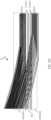
Images










Classifications
-
- G—PHYSICS
- G02—OPTICS
- G02F—OPTICAL DEVICES OR ARRANGEMENTS FOR THE CONTROL OF LIGHT BY MODIFICATION OF THE OPTICAL PROPERTIES OF THE MEDIA OF THE ELEMENTS INVOLVED THEREIN; NON-LINEAR OPTICS; FREQUENCY-CHANGING OF LIGHT; OPTICAL LOGIC ELEMENTS; OPTICAL ANALOGUE/DIGITAL CONVERTERS
- G02F1/00—Devices or arrangements for the control of the intensity, colour, phase, polarisation or direction of light arriving from an independent light source, e.g. switching, gating or modulating; Non-linear optics
- G02F1/01—Devices or arrangements for the control of the intensity, colour, phase, polarisation or direction of light arriving from an independent light source, e.g. switching, gating or modulating; Non-linear optics for the control of the intensity, phase, polarisation or colour
- G02F1/13—Devices or arrangements for the control of the intensity, colour, phase, polarisation or direction of light arriving from an independent light source, e.g. switching, gating or modulating; Non-linear optics for the control of the intensity, phase, polarisation or colour based on liquid crystals, e.g. single liquid crystal display cells
- G02F1/133—Constructional arrangements; Operation of liquid crystal cells; Circuit arrangements
- G02F1/1333—Constructional arrangements; Manufacturing methods
-
- G—PHYSICS
- G06—COMPUTING OR CALCULATING; COUNTING
- G06F—ELECTRIC DIGITAL DATA PROCESSING
- G06F3/00—Input arrangements for transferring data to be processed into a form capable of being handled by the computer; Output arrangements for transferring data from processing unit to output unit, e.g. interface arrangements
- G06F3/01—Input arrangements or combined input and output arrangements for interaction between user and computer
- G06F3/03—Arrangements for converting the position or the displacement of a member into a coded form
- G06F3/041—Digitisers, e.g. for touch screens or touch pads, characterised by the transducing means
-
- G—PHYSICS
- G06—COMPUTING OR CALCULATING; COUNTING
- G06F—ELECTRIC DIGITAL DATA PROCESSING
- G06F3/00—Input arrangements for transferring data to be processed into a form capable of being handled by the computer; Output arrangements for transferring data from processing unit to output unit, e.g. interface arrangements
- G06F3/01—Input arrangements or combined input and output arrangements for interaction between user and computer
- G06F3/03—Arrangements for converting the position or the displacement of a member into a coded form
- G06F3/041—Digitisers, e.g. for touch screens or touch pads, characterised by the transducing means
- G06F3/0416—Control or interface arrangements specially adapted for digitisers
- G06F3/04164—Connections between sensors and controllers, e.g. routing lines between electrodes and connection pads
-
- G—PHYSICS
- G06—COMPUTING OR CALCULATING; COUNTING
- G06F—ELECTRIC DIGITAL DATA PROCESSING
- G06F3/00—Input arrangements for transferring data to be processed into a form capable of being handled by the computer; Output arrangements for transferring data from processing unit to output unit, e.g. interface arrangements
- G06F3/01—Input arrangements or combined input and output arrangements for interaction between user and computer
- G06F3/03—Arrangements for converting the position or the displacement of a member into a coded form
- G06F3/041—Digitisers, e.g. for touch screens or touch pads, characterised by the transducing means
- G06F3/044—Digitisers, e.g. for touch screens or touch pads, characterised by the transducing means by capacitive means
- G06F3/0443—Digitisers, e.g. for touch screens or touch pads, characterised by the transducing means by capacitive means using a single layer of sensing electrodes
-
- G—PHYSICS
- G06—COMPUTING OR CALCULATING; COUNTING
- G06F—ELECTRIC DIGITAL DATA PROCESSING
- G06F3/00—Input arrangements for transferring data to be processed into a form capable of being handled by the computer; Output arrangements for transferring data from processing unit to output unit, e.g. interface arrangements
- G06F3/01—Input arrangements or combined input and output arrangements for interaction between user and computer
- G06F3/03—Arrangements for converting the position or the displacement of a member into a coded form
- G06F3/041—Digitisers, e.g. for touch screens or touch pads, characterised by the transducing means
- G06F3/044—Digitisers, e.g. for touch screens or touch pads, characterised by the transducing means by capacitive means
- G06F3/0446—Digitisers, e.g. for touch screens or touch pads, characterised by the transducing means by capacitive means using a grid-like structure of electrodes in at least two directions, e.g. using row and column electrodes
-
- G—PHYSICS
- G06—COMPUTING OR CALCULATING; COUNTING
- G06F—ELECTRIC DIGITAL DATA PROCESSING
- G06F2203/00—Indexing scheme relating to G06F3/00 - G06F3/048
- G06F2203/041—Indexing scheme relating to G06F3/041 - G06F3/045
- G06F2203/04103—Manufacturing, i.e. details related to manufacturing processes specially suited for touch sensitive devices
Definitions
- the disclosure relates to the field of semiconductor technology, in particular to a touch display panel and a display device.
- Narrow bezel for flexible multi-layer on cell (FMLOC) technology is also a challenge.
- Embodiments of the disclosure provide a touch display panel and a display device.
- the touch display panel includes: a base substrate, including: a display area, a bezel area surrounding the display area and a bonding area extending from the bezel area on one side; and a touch structural layer on a side of the base substrate.
- the touch structural layer includes a plurality of touch traces in the bezel area; and at least part of the touch traces are single-layered traces and adjacent single-layered touch traces are disposed in different layers.
- the bezel area includes a plurality of corner areas.
- the plurality of touch traces extend to the bonding area through at least one of the corner areas, in at least one of the corner areas, at least part of the touch traces are single-layered traces, and adjacent single-layered touch traces are disposed in different layers.
- adjacent single-layered touch traces are disposed in two conducting layers, and the touch traces respectively arranged in two conducting layers are arranged alternately.
- all the touch traces are distributed at a side of the first dam structure facing away from the bonding area.
- the touch traces include a first touch trace group arranged at a side of the first dam structure facing away from the bonding area, and a second touch trace group arranged at a side of the first dam structure close to the bonding area.
- the touch traces are single-layered traces, and adjacent single-layered touch traces are disposed in different layers.
- the touch traces are single-layered traces, and adjacent single-layered touch traces are disposed in different layers.
- the touch traces are single-layered traces, and adjacent single-layered touch traces are disposed in different layers.
- the touch traces include bridge trace parts correspondingly electrically connected to the respective touch traces in the second touch trace group, an orthographic projection of the bridge trace part on the base substrate has an overlapping area with an orthographic projection of the first dam structure on the base substrate, and an extending direction of the orthographic projection of the bridge trace part on the base substrate is intersected with the first direction; at least part of the bridge trace parts are single-layered traces, and adjacent single-layered bridge trace parts are disposed in different layers.
- the first touch trace group and the second touch trace group both include a plurality of first trace parts extending along the first direction; a center spacing between the adjacent bridge trace parts in an arrangement direction is greater than a center spacing between the adjacent first trace parts in the arrangement direction.
- the bezel area includes a first bezel area extending along the first direction and connected with the bonding area and a second bezel area; and the first dam structure is arranged in the first bezel area connected with the bonding area; and the touch trace includes second trace parts arranged in the second bezel area, and at least part of the second trace parts are double-layered traces.
- a center spacing between the adjacent second trace parts in an arrangement direction is greater than a center spacing between the adjacent first trace parts in the arrangement direction.
- the line width of the second trace part is substantially the same as the line width of the first trace part.
- a gap distance of adjacent second trace parts is greater than a gap distance of adjacent first trace parts.
- the line widths of all the first trace parts are the same.
- a center spacing between the adjacent first trace parts of the same layer in the arrangement direction is twice a center spacing between the adjacent first trace parts of different layers in the arrangement direction.
- the touch display panel further includes a plurality of touch electrodes arranged in the display area, and the touch electrodes are correspondingly electrically connected with the touch traces.
- the plurality of touch electrodes may include a plurality of driving units and a plurality of sensing units insulated from each other; the driving unit includes a plurality of driving electrodes arranged in line along the first direction, and a first connecting part electrically connecting two adjacent driving electrodes; and the sensing unit includes a plurality of sensing electrodes arranged in line along a direction vertical to the first direction, and a second connecting part electrically connecting two adjacent sensing electrodes.
- the touch display panel includes a first metal layer, an insulating layer and a second metal layer which are stacked in sequence, wherein a plurality of via holes are arranged in the insulating layer.
- a plurality of via holes are arranged in the insulating layer.
- one layer of the touch traces is disposed in the first metal layer, and the other layer of the touch traces is disposed in the second metal layer.
- Embodiments of the disclosure further provide a display device, wherein the touch display panel provided in embodiments of the disclosure is included.
- substantially or “substantially identical” as used herein includes the indicated values and is meant to be within an acceptable deviation range for specific values as determined by those skilled in the art when taking into account the measurements in discussion and errors associated with measurements of specific quantities (i.e., limitations of the measurement system). For example, “substantially identical” may mean that the difference with respect to the indicated value is in the range of one or more standard deviations or in the range of ⁇ 30%, 20%, 10%, 5%.
- IJP Ink jet print
- IJP Ink jet print
- a packaging process usually prints a layer of organic material with a large thickness on a panel as an organic packaging layer, and the organic material will level out to a certain distance outside the display area.
- the traditional FMLOC process requires the surrounding touch traces to be above the inside of the dam by a certain distance, thereby ensuring that the metal traces of FMLOC are in a flat area of IJP printing, and products with general bezel can be designed according to this rule.
- products with general bezel can be designed according to this rule.
- traces are difficult to be completely ensured to be above the dam.
- the bezel is too narrow, the space of traces is very small, traces not only may cross over the dam, but also be not completely accommodated in a limited space of the bezel.
- traces of the FMLOC including a driving line TX and a sensing line RX
- traces here are the densest, which is a big challenge to products.
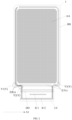
- the structure of the narrow-bezel product FMLOC is as shown in FIG. 1 , where the dotted circle indicates the left and right corners in the bottom of the screen.
- the lower left corner contains all the RX traces and part of the TX traces, and the traces here are the densest part of the whole screen, and the trace layout is greatly limited.
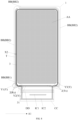
- the touch display panel includes:
- the bezel area BB includes a plurality of corner areas Y; the plurality of touch traces 2 extend to the bonding area CC through at least one of the corner areas Y. In at least one of the corner areas Y, at least part of the touch traces 2 are single-layered traces, and adjacent single-layered touch traces 2 are disposed in different layers.
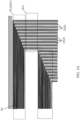
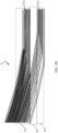
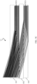
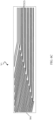
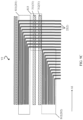
- FIG. 3A to FIG. 3C each shows an enlarged view of the touch trace 2 in the second corner area Y2 from left on the left side of the bottom bezel in FIG. 2
- FIG. 3B shows a schematic diagram of one of the trace layers in FIG. 3A
- FIG. 3C shows a schematic diagram of another trace layer in FIG. 3A
- the touch traces 2 may include a first layer of touch traces 21 and a second layer of touch traces 22, where the first layer of touch traces 21 and the second layer of touch traces 22 are disposed in different layers.
- the first layer of touch traces 21 is disposed in the first metal layer, as shown in FIG. 3B
- the second layer of touch traces 22 is disposed in the second metal layer, as shown in FIG. 3C
- the first layer of touch traces 21 and the second layer of touch traces 22 are disposed alternately.
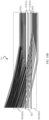
- FIG. 4A to FIG. 4C each is an enlarged view of the touch trace 2 in the first corner area Y1 from left on the left side of the bottom bezel in FIG. 2 , where FIG. 4B shows a schematic diagram of one of the trace layers in FIG. 4A , FIG. 4C shows a schematic diagram of another trace layer in FIG. 4A .
- the touch traces 2 may include a first layer of touch traces 21 and a second layer of touch traces 22, where the first layer of touch traces 21 and the second layer of touch traces 22 are disposed in different layers.
- the first layer of touch traces 21 is disposed in the first metal layer, as shown in FIG.
- the second layer of touch traces 22 is disposed in the second metal layer, as shown in FIG. 4C ; and the first layer of touch traces 21 and the second layer of touch traces 22 are disposed alternately.
- only part of the touch traces 2 in the lower part of the first corner area Y1 from left on the left side of the bottom bezel in FIG. 2 may be arranged to be single-layered traces, adjacent single-layered touch traces 2 are disposed in different layers, and touch traces 2 which are respectively disposed in two conducting layers are arranged alternately.
- FIG. 5A to FIG. 5C each is an enlarged view of the touch trace 2 in the first corner area Y1 from left on the left side of the bottom bezel in FIG. 2 , where FIG. 5B shows a schematic diagram of one of the trace layers in FIG. 5A , FIG. 5C shows a schematic diagram of another trace layer in FIG. 5A .
- the touch traces 2 may include a first layer of touch traces 21 and a second layer of touch traces 22, where the first layer of touch traces 21 and the second layer of touch traces 22 are disposed in different layers.
- the first layer of touch traces 21 is disposed in the first metal layer, as shown in FIG.
- the second layer of touch traces 22 is disposed in the second metal layer, as shown in FIG. 5C ; and the first layer of touch traces 21 and the second layer of touch traces 22 are arranged alternately.
- the upper touch traces 2 and lower the touch traces 2 in the first corner area Y1 from left on the left side of the bottom bezel in FIG. 2 may all be arranged to be single-layered traces, adjacent single-layered touch traces 2 are disposed in different layers.
- FIG. 6A to FIG. 6C each is an enlarged view of the touch trace 2 in the first corner area Y1 from left on the left side of the bottom bezel in FIG. 2 , where FIG. 6B shows a schematic diagram of one of the trace layers in FIG. 6A , FIG. 6C shows a schematic diagram of another trace layer in FIG. 6A .
- the touch traces 2 may include a first layer of touch traces 21 and a second layer of touch traces 22, where the first layer of touch traces 21 and the second layer of touch traces 22 are disposed in different layers.
- the first layer of touch traces 21 is disposed in the first metal layer, as shown in FIG.
- the second layer of touch traces 22 is disposed in the second metal layer, as shown in FIG. 6C ; and the first layer of touch traces 21 and the second layer of touch traces 22 are arranged alternately.
- only part of the touch traces 2 in the upper part of the first corner area Y1 from left on the left side of the bottom bezel in FIG. 2 may be arranged to be single-layered traces, and adjacent single-layered touch traces 2 are disposed in different layers.
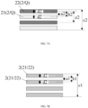
- At least part of the touch traces 2 are single-layered traces, and adjacent single-layered touch traces 2 are disposed in different layers. That is, in at least one corner area Y, at least part of the touch traces 2 are converted from double-layered traces to single-layered traces. Since adjacent single-layered touch traces 2 are disposed in different layers, the spacing between adjacent touch traces 2 in the same layer is relatively large. The probability of contact is low, the risk of poor manufacturing is low, and the center spacing can be reduced compared with the previous double layers (for example, as shown in FIG. 7A and FIG. 7B , where FIG. 7A is an enlarged view of a dotted circle X1 in FIG. 3A , and FIG.
- the touch display panel further includes a bending area DD, and the bonding area CC may also be provided with a first control chip IC1 and a second control chip IC2.
- the area of the side of the bending area CC facing away from the display area AA may be brought to a back side of the touch display panel by bending;
- the first control chip IC may be configured to control light emitting display of the display area;
- the second control chip IC2 may be configured to control the touch.
- adjacent single-layered touch traces 2 are disposed in two conducting layers.
- odd-numbered rows of touch traces 2 may be disposed in the first metal layer and even-numbered rows of touch traces 2 may be disposed in the second metal layer; alternatively, even-numbered rows of touch traces 2 may be disposed in the first metal layer and odd-numbered rows of touch traces 2 may be disposed in the second metal layer.
- adjacent single-layered touch traces 2 are arranged in two conducting layers, thereby realizing layout of a plurality of touch traces 2 in a smaller space, reducing the process risk, and further simplifying the wiring complexity of the touch traces 2.
- the touch display panel further includes a dam structure 3 between the base substrate 1 and the touch structural layer.
- the dam structure 3 includes a first dam structure 31 in the bezel area BB connected with the bonding area BB and extending along the first direction A1; and in at least one corner area Y, the touch traces 2 are at least distributed at a side of the first dam structure 31 facing away from the bonding area CC.
- the first dam structure 31 may include a plurality of sub-dam structures, for example, the first dam structure 31 may include a first sub-dam structure 311 and a second sub-dam structure 312, where the first sub-dam structure 311 may be disposed at a side of the second sub-dam structure 312 facing the display area AA.
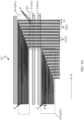
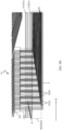
- FIG. 9A to FIG. 9C each is an enlarged view of the touch trace 2 in the second corner area Y2 from left on the left side of the bottom bezel of FIG. 8 , where FIG. 9B shows a schematic diagram of one of the trace layers in FIG. 9A , FIG. 9C shows a schematic diagram of another trace layer in FIG. 9A .
- the touch traces 2 may include a first layer of touch traces 21 and a second layer of touch traces 22, where the first layer of touch traces 21 and the second layer of touch traces 22 are disposed in different layers.
- the first layer of touch traces 21 is disposed in the first metal layer, as shown in FIG.
- the touch traces 2 may be divided into two groups, one of the groups (that is, the touch traces 2 in the upper dotted box S11 in FIG. 9A ) is distributed at a side of the first dam structure 31 facing away from the bonding area CC (that is, distributed above the first dam structure 31 in FIG. 9A ), and the other group (that is, the touch traces 2 in the lower dotted box S12 in FIG. 9A ) is distributed at a side of the first dam structure 31 facing the bonding area CC (that is, distributed below the first dam structure 31 in FIG. 9A ).
- the groups that is, the touch traces 2 in the upper dotted box S11 in FIG. 9A
- the other group that is, the touch traces 2 in the lower dotted box S12 in FIG. 9A
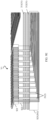
- FIG. 10A to FIG. 10C each is an enlarged view of the touch trace 2 in the first corner area Y1 from left on the left side of the bottom bezel of FIG. 8 , where FIG. 10B shows a schematic diagram of one of the trace layers in FIG. 10A , FIG. 10C shows a schematic diagram of another trace layer of FIG. 10A .
- the touch traces 2 may include a first layer of touch traces 21 and a second layer of touch traces 22, where the first layer of touch traces 21 and the second layer of touch traces 22 are disposed in different layers.
- the first layer of touch traces 21 is disposed in the first metal layer, as shown in FIG.
- the touch traces 2 may be divided into two groups, one of the groups (that is, the touch traces 2 in the upper dotted box S31 in FIG. 10A ) is distributed at a side of the first dam structure 31 facing away from the bonding area CC (that is, distributed above the first dam structure 31 in FIG. 10A ), and the other group (that is, the touch traces 2 in the lower dotted box S33 in FIG. 10A ) is distributed at a side of the first dam structure 31 facing the bonding area CC (that is, distributed below the first dam structure 31 in FIG. 10A ).
- the groups that is, the touch traces 2 in the upper dotted box S31 in FIG. 10A
- the other group that is, the touch traces 2 in the lower dotted box S33 in FIG. 10A
- FIG. 11A to FIG. 11C each is an enlarged view of the touch trace 2 in the first corner area Y1 from left on the left side of the bottom bezel of FIG. 8 , where FIG. 11B shows a schematic diagram of one of the trace layers in FIG. 11A , FIG. 11C shows a schematic diagram of another trace layer of FIG. 11A .
- the touch traces 2 may include a first layer of touch traces 21 and a second layer of touch traces 22, where the first layer of touch traces 21 and the second layer of touch traces 22 are disposed in different layers.
- the first layer of touch traces 21 is disposed in the first metal layer, as shown in FIG.
- the second layer of touch traces 22 is disposed in the second metal layer, as shown in FIG. 11C ; and the first layer of touch traces 21 and the second layer of touch traces 22 are arranged alternately.
- the touch traces 2 (such as the touch traces 2 in the dotted box S41 in FIG. 11A ) are all distributed at a side of the first dam structure 31 far away from the bonding area CC (such as above the first wall retaining structure 31 in FIG. 11A ).
- This embodiment can be applied to a case that there is a larger space in the area above the first dam structure 31, and the touch traces 2 are all designed at a side of the first dam structure 31 facing away from the bonding area CC, adjacent touch traces 2 are in different metal layers. In this case, in the same layer, the center spacing between adjacent touch traces 2 is large, thereby satisfying the process requirements.
- FIG. 12 is an enlarged view of the touch trace 2 in the first corner area Y3 from right on the right side of the bottom bezel of FIG. 8 , the touch traces 2 are double-layered traces.
- the touch traces 2 are divided into two groups, one of the groups (that is, the touch traces 2 in the upper dotted box S51 in FIG. 12 ) is distributed at a side of the first dam structure 31 facing away from the bonding area CC (that is, above the first dam structure 31 in FIG. 12 ), and the other group (that is, the touch traces 2 in the lower dotted box S52 in FIG.
- This embodiment may be applied to a touch display panel with the bottom bezel having a greater space than the bottom bezel in the aforementioned cases, and the touch traces 2 may all be designed to be double-layered metal, to reduce resistance.
- FIG. 9D to FIG. 9F each is an enlarged view of the touch trace 2 in the first corner area Y1 from left on the left side of the bottom bezel of FIG. 8 , where FIG. 9E shows a schematic diagram of one of the trace layers in FIG. 9D , FIG. 9F shows a schematic diagram of another trace layer in FIG. 9D .
- the touch traces 2 may include a first layer of touch traces 21 and a second layer of touch traces 22, where the first layer of touch traces 21 and the second layer of touch traces 22 are disposed in different layers.
- the first layer of touch traces 21 is disposed in the first metal layer, as shown in FIG.
- the second layer of touch traces 22 is disposed in the second metal layer, as shown in FIG. 9F ; and the first layer of touch traces 21 and the second layer of touch traces 22 are arranged alternately.
- the touch traces 2 may be distributed at a side of the first dam structure 31 facing the bonding area CC.
- all the touch traces 2 are distributed at a side of the first dam structure 31 facing away from the bonding area CC.
- all the touch traces 2 are distributed at a side of the first dam structure 31 facing away from the bonding area CC.
- the touch traces 2 in at least one corner area Y, include a first touch trace group 201 at a side of the first dam structure 31 facing away from the bonding area CC, and a second touch trace group 202 at a side of the first dam structure 31 close to the bonding area CC.
- the touch traces 2 are distributed at different sides of the first dam structure 31, thereby avoiding the risk of poor touch traces 2 due to limited wiring space of the touch traces 2 when the touch traces 2 are distributed at the side of the first dam structure 31 facing away from the bonding area CC.
- the touch traces 2 are distributed at different sides of the first dam structure 31, and include the first touch trace group 201 at a side of the first dam structure 31 facing away from the bonding area CC, and a second touch trace group 202 at a side of the first dam structure 31 facing away from the bonding area CC, thereby reducing the risk of poor touch traces 2.
- the touch traces 2 are distributed at different sides of the first dam structure 31, and include the first touch trace group 201 at a side of the first dam structure 31 facing away from the bonding area CC, and a second touch trace group 202 at a side, of the first dam structure 31 close to the bonding area CC, thereby reducing the risk of poor touch traces 2.
- the touch traces 2 are single-layered traces, and adjacent single-layered touch traces 2 are disposed in different layers.
- the second touch trace group 202 at least part of the touch traces 2 are single-layered traces, and adjacent single-layered touch traces 2 are disposed in different layers.
- the touch traces 2 are single-layered traces, and adjacent single-layered touch traces 2 are disposed in different layers.
- the touch traces 2 include bridge trace parts P correspondingly electrically connected to each of the touch traces 2 in the second touch trace group 202 (that is, the touch traces 2 in the dotted box S13 in the middle of FIG. 9A , the touch traces 2 in the dotted box S22 in the middle of FIG. 9D , and the touch traces 2 in the dotted box S32 in the middle of FIG. 10A ).
- An orthographic projection of the bridge trace part P on the base substrate 1 has an overlapping area with an orthographic projection of the first dam structure 31 on the base substrate 1, and an extending direction of the orthographic projection of the bridge trace part P on the base substrate 1 is intersected with the first direction A1; and at least part of the bridge trace parts P are single-layered traces, and adjacent single-layered bridge trace parts P are disposed in different layers.
- the bridge trace parts P may cross over the first dam structure 31 in a direction perpendicular to the dam structure or in a oblique direction relative to the dam structure.
- the extending direction of the bridge trace part P is perpendicular to the extending direction of the first dam structure 31.
- an included angle ⁇ facing towards the display area AA and formed between bridge trace part P and the first dam structure 31 is in a range of 90° to 180°.
- the first touch trace group 201 and the second touch trace group 202 both include a plurality of first trace parts Q extending along a first direction A1; in combination with FIG. 9A , a center spacing b3 of adjacent bridge trace parts P in their arrangement direction is greater than a center spacing b2 of adjacent first trace parts Q in their arrangement direction.
- a center spacing b3 of adjacent bridge trace parts P in their arrangement direction is greater than a center spacing b2 of adjacent first trace parts Q in their arrangement direction, due to a segment gap between the first dam structure 31 and the surrounding part, the line width of the bridge trace part P is large, thereby reducing the risk of broken traces or poor contact when the touch traces 2 cross over the first dam structure 31.
- the bezel area BB includes a first bezel area BB1 extending along a first direction A1 and connected with the bonding area CC and a second bezel area BB2.
- other bezel areas BB except the first bezel area BB1 may all serve as the second bezel area BB2, and the first dam structure 31 is located in the first bezel area BB1 connected with the bonding area CC.
- the touch traces 2 further include second trace parts T in the second bezel area BB, and at least part of the second trace parts T are double-layered traces.
- FIG. 13 is an enlarged view of the dotted circle X2 of FIG. 8
- a center spacing b4 of adjacent second trace parts T in their arrangement direction is greater than a center spacing b2 of adjacent first trace parts Q in their arrangement direction.
- a center spacing b2 of adjacent first trace parts Q in the arrangement direction may be reduced, to allow the first trace parts Q to have more wiring space.
- the line width d3 of the second trace part T is substantially the same as the line width d2 of the first trace part Q.
- the line width d3 of each second trace part T may be the same.
- a gap distance a3 of adjacent two trace parts T is greater than a gap distance a2 of adjacent first trace parts Q.
- the line widths d2 of all the first trace parts Q may be the same.
- a center spacing e2 of the adjacent first trace parts Q of the same layer in the arrangement direction is twice a center spacing b2 of the adjacent first trace parts Q of different layers in the arrangement direction.
- the touch display panel further includes a plurality of touch electrodes in the display area, and the touch electrodes are correspondingly electrically connected with the touch traces.
- a plurality of touch electrodes may include a plurality of driving units 510 and a plurality of sensing units 520 insulated from each other; each driving unit 510 includes a plurality of driving electrodes 511 arranged in line along the first direction A1, and first connecting parts 512 electrically connecting two adjacent driving electrodes 511; and each sensing unit 520 includes a plurality of sensing electrodes 521 arranged in line along a second direction A2, and a second connecting part 522 electrically connecting two adjacent sensing electrodes 521.
- the first direction A1 is intersected with the second direction A2. Specifically, the first direction A1 may be the row direction of arrangement of the driving electrodes 511, and the second direction A2 may be the column direction of arrangement of the driving electrodes 511.
- the touch traces 2 may include driving traces Tx and sensing traces Rx.
- One driving unit 510 may be correspondingly electrically connected with one driving trace Tx
- one sensing unit 520 may be correspondingly electrically connected with one sensing trace Rx.
- one driving unit 510 may correspond to one touch trace 2
- a plurality of touch traces 2 of a plurality of driving units 510 may be respectively arranged at two sides of the display area AA for wiring.
- the touch traces 2 corresponding to the driving unit 510 and the touch traces 2 corresponding to the sensing unit 520 may also be wired in other manners, which is not limited in the embodiments of the disclosure.
- a plurality of touch electrodes include a first metal layer 610, an insulating layer 620 and a second metal layer 630 which are stacked in sequence, and a plurality of via holes 621 in the insulating layer 620.
- the touch traces 2 are single-layered traces, and adjacent single-layered touch traces 2 are disposed in different layers.
- the touch traces 2 include a first layer of touch traces 21 and a second layer of touch traces 22.
- the first layer of touch traces 21 is disposed in the first metal layer 610; and the second layer of touch traces 22 is disposed in the second metal layer 630.
- the driving electrode 511, the first connecting part 512 and the sensing electrode 521 are disposed in one of the first metal layer 610 and the second metal layer 630
- the second connecting part 522 is disposed in another of the first metal layer 610 and the second metal layer 630
- the second connecting part 522 electrically connects two adjacent sensing electrodes 521 through via holes 621.
- the driving electrode 511, the second connecting part 522 and the sensing electrode 521 are disposed in one of the first metal layer 610 and the second metal layer 630, the first connecting part 512 is disposed in another of the first metal layer 610 and the second metal layer 630, and the first connecting part 512 electrically connects two adjacent driving electrodes 511 through via holes 621.
- the driving electrode 511, the sensing electrode 521, the first connecting part 512 and the second connecting part 522 include metal meshes. Specifically, at least part of the metal meshes may correspond to one or more pixels.
- the touch display panel may also include peripheral traces 7 arranged at a side of the touch trace 2 facing away from the display area AA.
- the peripheral traces 7 may be guard lines (Guard) configured to prevent signal interference between different driving traces Tx, between different sensing traces Rx and/or between driving traces Tx and sensing traces Rx, or, may also be ground lines (GND) configured to guide away electrostatic signals or electromagnetic signals.
- the peripheral traces 7 may adopt double-layered traces to have smaller resistance.
- the peripheral traces 7 may also be other signal lines, which is not limited in the embodiments of the disclosure.
- an embodiment of the disclosure further provides a display device, including the touch display panel provided in embodiments of the disclosure.
- At least part of the touch traces 2 are single-layered traces, and adjacent single-layered touch traces 2 are disposed in different layers, that is, in at least one corner area Y, at least part of the touch traces 2 are converted from double-layered traces to single-layered traces. Since adjacent single-layered touch traces 2 are disposed in different layers, the spacing between adjacent touch traces 2 in the same layer is relatively large. The probability of contact is low, the risk of poor manufacturing is low, and the center spacing can be compressed by the previous double layers (for example, in combination with FIG. 7A and FIG. 7B , where FIG. 7A is an enlarged view of a dotted circle in FIG. 3A , and FIG.
Landscapes
- Engineering & Computer Science (AREA)
- Physics & Mathematics (AREA)
- Theoretical Computer Science (AREA)
- General Engineering & Computer Science (AREA)
- General Physics & Mathematics (AREA)
- Human Computer Interaction (AREA)
- Nonlinear Science (AREA)
- Crystallography & Structural Chemistry (AREA)
- Optics & Photonics (AREA)
- Chemical & Material Sciences (AREA)
- Mathematical Physics (AREA)
- Computer Networks & Wireless Communication (AREA)
- Position Input By Displaying (AREA)
Applications Claiming Priority (1)
| Application Number | Priority Date | Filing Date | Title |
|---|---|---|---|
| PCT/CN2022/095313 WO2023225956A1 (fr) | 2022-05-26 | 2022-05-26 | Écran d'affichage tactile et dispositif d'affichage |
Publications (2)
| Publication Number | Publication Date |
|---|---|
| EP4517414A1 true EP4517414A1 (fr) | 2025-03-05 |
| EP4517414A4 EP4517414A4 (fr) | 2025-07-02 |
Family
ID=88918143
Family Applications (1)
| Application Number | Title | Priority Date | Filing Date |
|---|---|---|---|
| EP22943156.4A Pending EP4517414A4 (fr) | 2022-05-26 | 2022-05-26 | Écran d'affichage tactile et dispositif d'affichage |
Country Status (4)
| Country | Link |
|---|---|
| US (2) | US12353654B2 (fr) |
| EP (1) | EP4517414A4 (fr) |
| CN (1) | CN117460988A (fr) |
| WO (1) | WO2023225956A1 (fr) |
Families Citing this family (1)
| Publication number | Priority date | Publication date | Assignee | Title |
|---|---|---|---|---|
| EP4459445A4 (fr) * | 2022-08-29 | 2025-07-02 | Boe Technology Group Co Ltd | Écran d'affichage et dispositif d'affichage |
Family Cites Families (22)
| Publication number | Priority date | Publication date | Assignee | Title |
|---|---|---|---|---|
| CN103186276B (zh) | 2012-01-03 | 2016-01-20 | 天津富纳源创科技有限公司 | 印刷线路和触摸屏之印刷线路 |
| CN104635981B (zh) * | 2014-11-26 | 2018-06-22 | 业成光电(深圳)有限公司 | 触控模组及具有该触控模组的触控显示装置 |
| US10834815B2 (en) | 2015-12-01 | 2020-11-10 | Japan Aviation Electronics Industry, Limited | Printed wiring line, electronic device, touch panel, gravure plate, printed wiring line formation method, touch panel production method, and electronic device production method |
| CN105808027A (zh) | 2016-03-11 | 2016-07-27 | 惠州Tcl移动通信有限公司 | 一种触摸屏感应结构、触摸屏及窄边框电子显示设备 |
| CN107390941B (zh) * | 2017-08-17 | 2021-01-29 | 京东方科技集团股份有限公司 | 触控基板、触控面板、显示基板、显示面板和显示装置 |
| KR102526215B1 (ko) * | 2017-10-27 | 2023-04-26 | 엘지디스플레이 주식회사 | 터치패널 및 이를 포함하는 터치표시장치 |
| KR102588343B1 (ko) | 2017-10-27 | 2023-10-11 | 엘지디스플레이 주식회사 | 터치 디스플레이 장치 |
| CN207799654U (zh) | 2018-02-22 | 2018-08-31 | 蓝思科技(长沙)有限公司 | 一种触控屏边框 |
| CN108415601B (zh) | 2018-03-12 | 2020-12-25 | 京东方科技集团股份有限公司 | 布线结构及其制造方法、显示装置 |
| CN108958562A (zh) * | 2018-07-13 | 2018-12-07 | 京东方科技集团股份有限公司 | 触控屏及其制作方法、显示装置 |
| CN111373356B (zh) | 2018-10-26 | 2024-01-23 | 京东方科技集团股份有限公司 | 触控基板、触控显示装置、制造触控基板的方法 |
| CN109491546B (zh) | 2018-12-25 | 2020-12-25 | 武汉华星光电半导体显示技术有限公司 | 一种窄边框触摸面板与制造方法 |
| CN110187797B (zh) | 2019-05-31 | 2022-02-01 | 京东方科技集团股份有限公司 | 触控显示面板 |
| CN110275650B (zh) * | 2019-06-27 | 2022-03-29 | 昆山国显光电有限公司 | 触摸感应装置、触控显示面板及触控显示面板母板 |
| CN110515505B (zh) | 2019-08-29 | 2024-06-18 | 京东方科技集团股份有限公司 | 一种触控基板及其制作方法、触控面板 |
| WO2021203360A1 (fr) * | 2020-04-09 | 2021-10-14 | 京东方科技集团股份有限公司 | Panneau d'affichage et dispositif d'affichage |
| KR102950990B1 (ko) * | 2020-06-08 | 2026-04-09 | 엘지디스플레이 주식회사 | 터치 디스플레이 장치 |
| CN114153336B (zh) * | 2020-09-08 | 2026-01-06 | 京东方科技集团股份有限公司 | 触控结构、触控显示基板和触控显示装置 |
| US11460949B2 (en) | 2020-11-06 | 2022-10-04 | Au Optronics Corporation | Electronic device |
| CN112612371B (zh) * | 2020-12-15 | 2024-01-23 | 武汉天马微电子有限公司 | 触控显示面板及触控显示装置 |
| CN112965638B (zh) | 2021-04-23 | 2024-03-15 | 京东方科技集团股份有限公司 | 触控显示面板及显示装置 |
| CN114442858B (zh) * | 2022-02-25 | 2024-04-05 | 武汉天马微电子有限公司 | 一种触控显示面板和触控显示装置 |
-
2022
- 2022-05-26 EP EP22943156.4A patent/EP4517414A4/fr active Pending
- 2022-05-26 US US18/027,495 patent/US12353654B2/en active Active
- 2022-05-26 WO PCT/CN2022/095313 patent/WO2023225956A1/fr not_active Ceased
- 2022-05-26 CN CN202280001449.2A patent/CN117460988A/zh active Pending
-
2025
- 2025-06-11 US US19/234,404 patent/US20250306696A1/en active Pending
Also Published As
| Publication number | Publication date |
|---|---|
| CN117460988A (zh) | 2024-01-26 |
| WO2023225956A1 (fr) | 2023-11-30 |
| US20240295932A1 (en) | 2024-09-05 |
| US20250306696A1 (en) | 2025-10-02 |
| US12353654B2 (en) | 2025-07-08 |
| EP4517414A4 (fr) | 2025-07-02 |
Similar Documents
| Publication | Publication Date | Title |
|---|---|---|
| CN214586834U (zh) | 显示基板及显示装置 | |
| CN113554969B (zh) | 显示面板及显示装置 | |
| US10558312B2 (en) | Touch panel | |
| US12057382B2 (en) | Chip on film assembly, display panel, and display module | |
| JP2024505314A (ja) | 表示基板および表示装置 | |
| CN112114707A (zh) | 显示面板及其驱动方法和制备方法、显示装置 | |
| KR20180131768A (ko) | 터치 디스플레이 장치, 터치 디스플레이 패널 및 터치 디스플레이 패널의 제조 방법 | |
| US12026335B2 (en) | Touch display panel with reduced impedance of touch signal line | |
| US11189584B2 (en) | Driving chip including bonding pads in non-display area and display panel | |
| US20250306696A1 (en) | Touch display panel and display device | |
| US12073049B2 (en) | Display panel and display apparatus with additional electrode layer for improving mutual capacitance variation | |
| US20230289001A1 (en) | Display panel and display device | |
| CN113467650A (zh) | 触控显示面板及显示装置 | |
| US20240302930A1 (en) | Touch-control display panel, touch-control display apparatus and method for manufacturing touch-control layer | |
| CN113867572B (zh) | 显示面板及显示装置 | |
| CN115884636A (zh) | 显示面板 | |
| US8867229B2 (en) | Printed circuit and printed circuit of touch panel | |
| US8780067B1 (en) | Bridging structure for signal transmission of touch panel | |
| JP5517718B2 (ja) | 電極基板、タッチパネル装置および表示装置 | |
| US8576575B2 (en) | Printed circuit and printed circuit of touch panel | |
| CN114779954A (zh) | 一种触控面板和显示装置 | |
| US12373052B2 (en) | Display panel and display apparatus | |
| US20250107357A1 (en) | Oled display panels and terminal devices | |
| US12254157B2 (en) | Touch display panel and electronic product | |
| CN113655903B (zh) | 一种显示面板及显示装置 |
Legal Events
| Date | Code | Title | Description |
|---|---|---|---|
| STAA | Information on the status of an ep patent application or granted ep patent |
Free format text: STATUS: THE INTERNATIONAL PUBLICATION HAS BEEN MADE |
|
| PUAI | Public reference made under article 153(3) epc to a published international application that has entered the european phase |
Free format text: ORIGINAL CODE: 0009012 |
|
| STAA | Information on the status of an ep patent application or granted ep patent |
Free format text: STATUS: REQUEST FOR EXAMINATION WAS MADE |
|
| 17P | Request for examination filed |
Effective date: 20241129 |
|
| AK | Designated contracting states |
Kind code of ref document: A1 Designated state(s): AL AT BE BG CH CY CZ DE DK EE ES FI FR GB GR HR HU IE IS IT LI LT LU LV MC MK MT NL NO PL PT RO RS SE SI SK SM TR |
|
| A4 | Supplementary search report drawn up and despatched |
Effective date: 20250602 |
|
| RIC1 | Information provided on ipc code assigned before grant |
Ipc: G06F 3/044 20060101ALI20250526BHEP Ipc: G06F 3/041 20060101ALI20250526BHEP Ipc: G02F 1/1333 20060101AFI20250526BHEP |
|
| DAV | Request for validation of the european patent (deleted) | ||
| DAX | Request for extension of the european patent (deleted) |