EP4517810A1 - Boîtier de semi-conducteur et procédé de fabrication d'un boîtier de semi-conducteur - Google Patents
Boîtier de semi-conducteur et procédé de fabrication d'un boîtier de semi-conducteur Download PDFInfo
- Publication number
- EP4517810A1 EP4517810A1 EP23194541.1A EP23194541A EP4517810A1 EP 4517810 A1 EP4517810 A1 EP 4517810A1 EP 23194541 A EP23194541 A EP 23194541A EP 4517810 A1 EP4517810 A1 EP 4517810A1
- Authority
- EP
- European Patent Office
- Prior art keywords
- encapsulation
- semiconductor package
- recess
- substrate
- semiconductor
- Prior art date
- Legal status (The legal status is an assumption and is not a legal conclusion. Google has not performed a legal analysis and makes no representation as to the accuracy of the status listed.)
- Withdrawn
Links
Images


Classifications
-
- H—ELECTRICITY
- H10—SEMICONDUCTOR DEVICES; ELECTRIC SOLID-STATE DEVICES NOT OTHERWISE PROVIDED FOR
- H10W—GENERIC PACKAGES, INTERCONNECTIONS, CONNECTORS OR OTHER CONSTRUCTIONAL DETAILS OF DEVICES COVERED BY CLASS H10
- H10W40/00—Arrangements for thermal protection or thermal control
- H10W40/70—Fillings or auxiliary members in containers or in encapsulations for thermal protection or control
- H10W40/77—Auxiliary members characterised by their shape
- H10W40/778—Auxiliary members characterised by their shape in encapsulations
-
- H—ELECTRICITY
- H10—SEMICONDUCTOR DEVICES; ELECTRIC SOLID-STATE DEVICES NOT OTHERWISE PROVIDED FOR
- H10W—GENERIC PACKAGES, INTERCONNECTIONS, CONNECTORS OR OTHER CONSTRUCTIONAL DETAILS OF DEVICES COVERED BY CLASS H10
- H10W74/00—Encapsulations, e.g. protective coatings
- H10W74/10—Encapsulations, e.g. protective coatings characterised by their shape or disposition
- H10W74/111—Encapsulations, e.g. protective coatings characterised by their shape or disposition the semiconductor body being completely enclosed
Definitions
- the present invention relates to the cooling of semiconductor packages, in particular of high voltage semiconductor packages.
- a semiconductor package may comprise one or more semiconductor dies mounted on a substrate/die pad.
- An encapsulation e.g., mold compound, encapsulates the semiconductor dies and the substrate. High switching speed and/or high currents lead to the generation of heat during operation.
- parts of the substrate may be exposed from the encapsulation.
- a heat sink may be mounted on the encapsulation comprising the exposed substrate part, also referred as exposed pad via a thin layer of a thermal interface material that provides electrical isolation.
- high voltage class products also need to fulfill creepage distance requirements while keeping the thermal characteristics at a high level. Exposed pads may thus not be desirable or even optional.
- Packages with heat transfer through mold compound are however limited in the ability to transfer thermal energy into the surrounding environment. Improved semiconductor packages and improved methods for manufacturing semiconductor packages may help to overcome these and other problems.
- a semiconductor package comprises a substrate and a semiconductor die mounted to a first surface of the substrate.
- the semiconductor package further comprises an encapsulation encapsulating the semiconductor die and the substrate.
- the encapsulation comprises a recess at an outer surface of the encapsulation.
- a material fills up the recess, wherein the material has a higher thermal conductivity than the encapsulation, wherein the material is electrically isolated from the substrate and the semiconductor die.
- a method for producing a semiconductor package comprising:
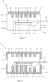
- Figure 1 shows a cross-section of a semiconductor package 100 comprising a semiconductor die 108 having a top side 160 and a bottom side 162 opposite to the top side 160.
- the bottom side 162 of the semiconductor die 108 is mounted on a first surface 106 of a substrate 102 by an interconnection 130, e.g., but not limited to a sintered, soldered, or welded interconnection.
- the substrate 102 comprises a second surface 104 opposite to the first surface 106.
- the top side 160 of the semiconductor die 108 is electrically connected to an external terminal 112, e.g., but not limited to via bond wires or ribbons 140, or a clip (not shown in Figure 1 bit indicated in Figure 3 and described in connection with Figure 3 herein below).
- the substrate 102 is electrically connected to a further external terminal (not shown in Figure 1 ) laterally adjacent to the external terminal 112.
- the substrate 102 may be monolithically formed with the further external terminal e.g., as part of a contiguous leadframe.
- An encapsulation 114 fully encapsulates the semiconductor die 108 and the substrate 102 providing electrical insulation. All external terminals are partially exposed from the encapsulation 114 providing electrical connection with e.g., a printed circuit board, a busbar etc.
- An outer surface 122 of the encapsulation 114 comprises recesses 110 with a certain depth and a lateral expansion.
- the depth of the recesses 110 is measured orthogonal to the outer surface 122 of the encapsulation 114.
- the depth of the respective recesses may be the same (as shown in Figure 1 ) or varying (as describe in more detail in the following).
- a material 116 with thermal conductivity higher than that of the encapsulation 114 is inserted into the recesses 110 and fills up the recesses 110.
- the material 116 may comprise or consist of a metal such as but not limited to silver, copper or aluminum.
- the material 116 may exceed the depth of the recesses 110 forming a contiguous layer 150 on the outer surface 122 of the encapsulation 114 and interconnecting the recesses 110.
- the material 116 can be disposed over the outer surface 122 of the encapsulation 114 filling the recesses 110 and/or forming the contiguous layer 150 using methods such as but not limited to pulsed laser deposition, aerosol jet printing, cold spray coating, printing (stencil, screen, impulse printing etc.) with or without transparent carrier, plateable mold compound, electrochemical deposition, electroless seed layer (Pd activated surface).
- a cooler may be mounted on the main surface 118 of the contiguous layer 150.
- the main surface 118 of the contiguous layer 150 may form a wall of the cooler, wherein the main surface 118 of the contiguous layer 150 may be in direct contact with a coolant flowing inside the cooler.
- the encapsulation 114 which is usually a resin or epoxy material has a lower thermal conductivity as compared to the material 116.
- Typical epoxy encapsulations have a thermal conductivity of less than 1W/mK, wherein metals such as silver, copper or aluminum have a thermal conductivity in the range of 300-450W/mK.
- the recesses 110 filled with the material 116 can be positioned close to the substrate 102, the semiconductor die 108 and/or bond wires or ribbons 140 to more effectively dissipate the heat.
- the lateral width and the depth of the recesses 110 can be chosen in a flexible manner depending on the heat generation inside the package 100 to optimize the heat transfer while maintaining the electrical insulation of the material 116.
- This concept can be used for semiconductor packages comprising a single semiconductor die or multiple semiconductor dies mounted on the same or multiple substrates, in which multiple semiconductor dies are arranged above or lateral to each other within the semiconductor package.
- the recesses 110 are formed on the first side 126 of the outer surface 122 of the encapsulation 114 facing the second surface 104 of the substrate 102 while maintaining electrical insulation from the substrate 102.
- Figure 2 shows a cross-sectional view of a semiconductor package 200 which is similar to the semiconductor package 100 and will only be described with regard to the differences from the semiconductor package 100 in the following.
- the contiguous layer 150 extends on the first 124a and a second side 124b of the outer surface 122 of the encapsulation 114.
- the first side 124a of the outer surface 122 of the encapsulation 114 is only partially covered by the contiguous layer 150 keeping the required distances from all the external terminals 112 with regard to electrical insulation.
- the semiconductor package 200 shown in Figure 2 has further recesses 234 on the second side 128 of the outer surface 122 of the encapsulation 114 facing the semiconductor die 108 and/or the bond wires or ribbons 140.
- the recesses 234 may have a different depth and a width as compared with the recesses 110.
- the recesses 234 are also filled with the material 116 as described in the previous examples.
- the depth and the width of the recesses 234 is again such that the material 116 is electrically insulated from the semiconductor die 108 and bond wires or ribbons 140.
- the material 116 may exceed the depth of the recesses 234 forming a contiguous layer 250 on the second side 128 of the outer surface 122 of the encapsulation 114.
- the contiguous layer 250 may be extended to the first 124a and the second side 124b of the side wall 124 of the outer surface 122 of the encapsulation 114 similar to the contiguous layer 150 of the semiconductor package 100 of Figure 1 .
- the contiguous layers 150 and 250 may join on the second side 124b of the side wall 124 of the outer surface 122 of the encapsulation 114.
- the semiconductor package 200 may have recesses 244 similar to the recesses 234 but the recesses 244 may have a different depth and/or lateral expansion as compared to the recesses 234 and/or the recesses 110.
- FIG 3 shows a cross-sectional view of a semiconductor package 300, wherein the semiconductor package 300 is similar to the semiconductor package 200 of Figure 2 and will be described only with regard to the differences to Figure 2 in the following.
- a clip 302 provides the connection.
- a section 304 of the clip 302 covers and is electrically connected with the top side 160 of the semiconductor die 108 via the interconnection 130.
- the clip 302 may be integrally formed with the external 112, or it may be formed separately from and connected to the external terminal 112 by soldering, sintering, or other suitable methods. Due to a uniform distance between the section 304 of the clip 302 and the second side 128 of the outer surface 128 of the encapsulation 114, recesses 234 with the uniform depth can be formed.
- the contiguous layers 150 and 250 are exemplary shown as joint in this embodiment at the second side 124b of the side wall 124 of the outer surface 122 of the encapsulation 114.
- Figure 4A shows a cross-sectional view of the semiconductor package 400, wherein the semiconductor package 400 is similar to the semiconductor package 100 of Figure 1 and will be described only with regard to the differences to Figure 1 in the following.
- the examples shown in Figures 1-3 have outer leads only on one side of the side wall 124 of the encapsulation, e.g., for instance as in TO-like semiconductor packages
- the example in Figure 4 comprises external terminals protruding out from both opposing sides 124a and 124c of the side wall 124 of the outer surface 122 of the encapsulation 114 such as but not limited to DSO-like semiconductor packages.
- the external terminal 112 may be electrically connected to the top side 160 of the semiconductor die 108 via bond wires or ribbons 140 or a clip as shown in the previous examples.
- a further external terminal 404 protruding from the opposite side of the external terminal 112 is electrically connected to substrate 102 via bond wires or ribbons 140, clips or a monolithically formed connection.
- Figure 4B shows a top view of the semiconductor package 400 of Figure 4A .
- the recesses are formed as a plurality of vias 432 with a limited lateral dimension, e.g., circular or squared.
- the plurality of vias 432 may be distributed across the first side 126 of the outer surface 122 of the encapsulation 114 uniformly or non-uniformly.
- the number of vias formed close to a part of the substrate comprising the semiconductor die 108 may be increased with regard to the periphery.
- Each via in the plurality of vias 432 may have a different depth and/or lateral expansion from the neighboring via.
- the contiguous layer 150 interconnects each via in the plurality of vias 432.
- the second side 128 of the outer surface 122 of the encapsulation 114 may also have a plurality of vias similar to the plurality of vias 432.
- the plurality of vias 432 and the plurality of trenches 436 shown in Fig 4B and 4C respectively can be formed by but not limited to e.g., a cavity in the mold tool, dicing or laser dicing.
- the semiconductor die may be manufactured from specific semiconductor material such as, for example, Si, SiC, SiGe, GaAs, GaN, AlGaN, InGaAs, InAIAs, etc., and, furthermore, may contain inorganic and/or organic materials that are not semiconductors.
- the semiconductor die may be of different types and may be manufactured by different technologies.
- the semiconductor package described herein includes a substrate.
- the substrate may form a part of a structured metal sheet such as, e.g., a leadframe.
- the substrate, the semiconductor die and the external terminal may at least partly be surrounded or embedded in an encapsulant.
- the encapsulant may form part of the periphery of the semiconductor package, i.e., may at least partly define the shape of the semiconductor package.
- the encapsulant may be an electrically insulating material and may comprise or be a thermoset material or a thermoplastic material.
- a thermoset material may, e.g., be made on the basis of an epoxy resin, a silicone resin or an acrylic resin.
- a thermoplastic material may, e.g., comprise one or more materials selected from the group of polyetherimide (PEI), polyether-sulfone (PES), polyphenylene-sulfide (PPS), polyamide-imide (PAI), and polyethylene-terephthalate (PET).
- PEI polyetherimide
- PES polyether-sulfone
- PPS polyphenylene-sulfide
- PAI polyamide-imide
- PET polyethylene-terephthalate
- the encapsulant may include or be a polymer material, e.g., a duroplastic polymer material.
- the encapsulant may include or be at least one of a filled or unfilled mold material, a filled or unfilled thermoplastic material, a filled or unfilled thermoset material, a filled or unfilled laminate, a fiber-reinforced laminate, a fiber-reinforced polymer laminate, and a fiber-reinforced polymer laminate with filler particles.
- an electronic device in accordance with the disclosure may constitute, e.g., an engine control unit (ECU), a power supply, a DC-DC voltage converter, an AC-DC voltage converter, a power amplifier, and many other devices, in particular power devices.
- ECU engine control unit
- a power supply e.g., a DC-DC voltage converter, an AC-DC voltage converter, a power amplifier, and many other devices, in particular power devices.
Landscapes
- Structures Or Materials For Encapsulating Or Coating Semiconductor Devices Or Solid State Devices (AREA)
Priority Applications (1)
| Application Number | Priority Date | Filing Date | Title |
|---|---|---|---|
| EP23194541.1A EP4517810A1 (fr) | 2023-08-31 | 2023-08-31 | Boîtier de semi-conducteur et procédé de fabrication d'un boîtier de semi-conducteur |
Applications Claiming Priority (1)
| Application Number | Priority Date | Filing Date | Title |
|---|---|---|---|
| EP23194541.1A EP4517810A1 (fr) | 2023-08-31 | 2023-08-31 | Boîtier de semi-conducteur et procédé de fabrication d'un boîtier de semi-conducteur |
Publications (1)
| Publication Number | Publication Date |
|---|---|
| EP4517810A1 true EP4517810A1 (fr) | 2025-03-05 |
Family
ID=87889305
Family Applications (1)
| Application Number | Title | Priority Date | Filing Date |
|---|---|---|---|
| EP23194541.1A Withdrawn EP4517810A1 (fr) | 2023-08-31 | 2023-08-31 | Boîtier de semi-conducteur et procédé de fabrication d'un boîtier de semi-conducteur |
Country Status (1)
| Country | Link |
|---|---|
| EP (1) | EP4517810A1 (fr) |
Citations (3)
| Publication number | Priority date | Publication date | Assignee | Title |
|---|---|---|---|---|
| JPH03171651A (ja) * | 1989-11-29 | 1991-07-25 | Seiko Epson Corp | 半導体装置 |
| US20170358556A1 (en) * | 2016-06-13 | 2017-12-14 | Micron Technology, Inc. | Semiconductor device assembly with through-mold cooling channel formed in encapsulant |
| US11171067B2 (en) * | 2017-03-13 | 2021-11-09 | Murata Manufacturing Co., Ltd. | Module having a sealing resin layer with radiating member filled depressions |
-
2023
- 2023-08-31 EP EP23194541.1A patent/EP4517810A1/fr not_active Withdrawn
Patent Citations (3)
| Publication number | Priority date | Publication date | Assignee | Title |
|---|---|---|---|---|
| JPH03171651A (ja) * | 1989-11-29 | 1991-07-25 | Seiko Epson Corp | 半導体装置 |
| US20170358556A1 (en) * | 2016-06-13 | 2017-12-14 | Micron Technology, Inc. | Semiconductor device assembly with through-mold cooling channel formed in encapsulant |
| US11171067B2 (en) * | 2017-03-13 | 2021-11-09 | Murata Manufacturing Co., Ltd. | Module having a sealing resin layer with radiating member filled depressions |
Similar Documents
| Publication | Publication Date | Title |
|---|---|---|
| KR102585450B1 (ko) | 브레이징된 전기 전도성 층을 포함하는 칩 캐리어를 구비한 몰딩된 패키지 | |
| US7846779B2 (en) | Power device package and method of fabricating the same | |
| CN102593081B (zh) | 包括散热器的半导体器件 | |
| US10727151B2 (en) | Semiconductor chip package having a cooling surface and method of manufacturing a semiconductor package | |
| US20230215788A1 (en) | Power module and manufacturing method thereof, converter, and electronic device | |
| US9385107B2 (en) | Multichip device including a substrate | |
| US20090244848A1 (en) | Power Device Substrates and Power Device Packages Including the Same | |
| US20160365296A1 (en) | Electronic Devices with Increased Creepage Distances | |
| US10079195B2 (en) | Semiconductor chip package comprising laterally extending connectors | |
| US11587855B2 (en) | Method of attaching an insulation sheet to encapsulated semiconductor device | |
| US20240250004A1 (en) | Method for fabricating a semiconductor device including an embedded semiconductor die | |
| JP2019071412A (ja) | チップパッケージ | |
| US20220310475A1 (en) | Electronic packages with integral heat spreaders | |
| US11626351B2 (en) | Semiconductor package with barrier to contain thermal interface material | |
| US20090127681A1 (en) | Semiconductor package and method of fabricating the same | |
| US20160021780A1 (en) | Carrier, Semiconductor Module and Fabrication Method Thereof | |
| US9263421B2 (en) | Semiconductor device having multiple chips mounted to a carrier | |
| US20240243031A1 (en) | Thermal Enhanced Power Semiconductor Package | |
| US12068226B2 (en) | Semiconductor assembly with multi-device cooling | |
| JP2007305772A (ja) | 半導体装置および半導体装置の製造方法 | |
| CN105990275A (zh) | 功率模块封装件及其制作方法 | |
| EP4517810A1 (fr) | Boîtier de semi-conducteur et procédé de fabrication d'un boîtier de semi-conducteur | |
| US20210066174A1 (en) | Semiconductor device package assemblies and methods of manufacture | |
| KR20260030700A (ko) | 플립 칩 및 사전 성형 클립 전력 모듈 | |
| EP4243058A1 (fr) | Boîtier de semi-conducteur et module de dispositif semi-conducteur le comprenant |
Legal Events
| Date | Code | Title | Description |
|---|---|---|---|
| PUAI | Public reference made under article 153(3) epc to a published international application that has entered the european phase |
Free format text: ORIGINAL CODE: 0009012 |
|
| STAA | Information on the status of an ep patent application or granted ep patent |
Free format text: STATUS: THE APPLICATION HAS BEEN PUBLISHED |
|
| AK | Designated contracting states |
Kind code of ref document: A1 Designated state(s): AL AT BE BG CH CY CZ DE DK EE ES FI FR GB GR HR HU IE IS IT LI LT LU LV MC ME MK MT NL NO PL PT RO RS SE SI SK SM TR |
|
| STAA | Information on the status of an ep patent application or granted ep patent |
Free format text: STATUS: THE APPLICATION IS DEEMED TO BE WITHDRAWN |
|
| 18D | Application deemed to be withdrawn |
Effective date: 20250906 |