EP4517837A1 - Photovoltaische zelle mit spezifischer anordnung von energiekollektoren und verfahren zur herstellung einer solchen zelle - Google Patents
Photovoltaische zelle mit spezifischer anordnung von energiekollektoren und verfahren zur herstellung einer solchen zelle Download PDFInfo
- Publication number
- EP4517837A1 EP4517837A1 EP23193763.2A EP23193763A EP4517837A1 EP 4517837 A1 EP4517837 A1 EP 4517837A1 EP 23193763 A EP23193763 A EP 23193763A EP 4517837 A1 EP4517837 A1 EP 4517837A1
- Authority
- EP
- European Patent Office
- Prior art keywords
- layer
- photovoltaic cell
- positive
- peripheral bus
- negative
- Prior art date
- Legal status (The legal status is an assumption and is not a legal conclusion. Google has not performed a legal analysis and makes no representation as to the accuracy of the status listed.)
- Pending
Links
Images



Classifications
-
- H—ELECTRICITY
- H10—SEMICONDUCTOR DEVICES; ELECTRIC SOLID-STATE DEVICES NOT OTHERWISE PROVIDED FOR
- H10F—INORGANIC SEMICONDUCTOR DEVICES SENSITIVE TO INFRARED RADIATION, LIGHT, ELECTROMAGNETIC RADIATION OF SHORTER WAVELENGTH OR CORPUSCULAR RADIATION
- H10F77/00—Constructional details of devices covered by this subclass
- H10F77/20—Electrodes
- H10F77/206—Electrodes for devices having potential barriers
- H10F77/211—Electrodes for devices having potential barriers for photovoltaic cells
- H10F77/215—Geometries of grid contacts
-
- H—ELECTRICITY
- H10—SEMICONDUCTOR DEVICES; ELECTRIC SOLID-STATE DEVICES NOT OTHERWISE PROVIDED FOR
- H10F—INORGANIC SEMICONDUCTOR DEVICES SENSITIVE TO INFRARED RADIATION, LIGHT, ELECTROMAGNETIC RADIATION OF SHORTER WAVELENGTH OR CORPUSCULAR RADIATION
- H10F19/00—Integrated devices, or assemblies of multiple devices, comprising at least one photovoltaic cell covered by group H10F10/00, e.g. photovoltaic modules
- H10F19/80—Encapsulations or containers for integrated devices, or assemblies of multiple devices, having photovoltaic cells
-
- H—ELECTRICITY
- H10—SEMICONDUCTOR DEVICES; ELECTRIC SOLID-STATE DEVICES NOT OTHERWISE PROVIDED FOR
- H10F—INORGANIC SEMICONDUCTOR DEVICES SENSITIVE TO INFRARED RADIATION, LIGHT, ELECTROMAGNETIC RADIATION OF SHORTER WAVELENGTH OR CORPUSCULAR RADIATION
- H10F77/00—Constructional details of devices covered by this subclass
- H10F77/93—Interconnections
- H10F77/933—Interconnections for devices having potential barriers
- H10F77/935—Interconnections for devices having potential barriers for photovoltaic devices or modules
- H10F77/937—Busbar structures for modules
-
- H—ELECTRICITY
- H10—SEMICONDUCTOR DEVICES; ELECTRIC SOLID-STATE DEVICES NOT OTHERWISE PROVIDED FOR
- H10F—INORGANIC SEMICONDUCTOR DEVICES SENSITIVE TO INFRARED RADIATION, LIGHT, ELECTROMAGNETIC RADIATION OF SHORTER WAVELENGTH OR CORPUSCULAR RADIATION
- H10F19/00—Integrated devices, or assemblies of multiple devices, comprising at least one photovoltaic cell covered by group H10F10/00, e.g. photovoltaic modules
- H10F19/30—Integrated devices, or assemblies of multiple devices, comprising at least one photovoltaic cell covered by group H10F10/00, e.g. photovoltaic modules comprising thin-film photovoltaic cells
- H10F19/31—Integrated devices, or assemblies of multiple devices, comprising at least one photovoltaic cell covered by group H10F10/00, e.g. photovoltaic modules comprising thin-film photovoltaic cells having multiple laterally adjacent thin-film photovoltaic cells deposited on the same substrate
- H10F19/37—Integrated devices, or assemblies of multiple devices, comprising at least one photovoltaic cell covered by group H10F10/00, e.g. photovoltaic modules comprising thin-film photovoltaic cells having multiple laterally adjacent thin-film photovoltaic cells deposited on the same substrate comprising means for obtaining partial light transmission through the integrated devices, or the assemblies of multiple devices, e.g. partially transparent thin-film photovoltaic modules for windows
-
- H—ELECTRICITY
- H10—SEMICONDUCTOR DEVICES; ELECTRIC SOLID-STATE DEVICES NOT OTHERWISE PROVIDED FOR
- H10F—INORGANIC SEMICONDUCTOR DEVICES SENSITIVE TO INFRARED RADIATION, LIGHT, ELECTROMAGNETIC RADIATION OF SHORTER WAVELENGTH OR CORPUSCULAR RADIATION
- H10F71/00—Manufacture or treatment of devices covered by this subclass
- H10F71/10—Manufacture or treatment of devices covered by this subclass the devices comprising amorphous semiconductor material
-
- H—ELECTRICITY
- H10—SEMICONDUCTOR DEVICES; ELECTRIC SOLID-STATE DEVICES NOT OTHERWISE PROVIDED FOR
- H10F—INORGANIC SEMICONDUCTOR DEVICES SENSITIVE TO INFRARED RADIATION, LIGHT, ELECTROMAGNETIC RADIATION OF SHORTER WAVELENGTH OR CORPUSCULAR RADIATION
- H10F71/00—Manufacture or treatment of devices covered by this subclass
- H10F71/10—Manufacture or treatment of devices covered by this subclass the devices comprising amorphous semiconductor material
- H10F71/103—Manufacture or treatment of devices covered by this subclass the devices comprising amorphous semiconductor material including only Group IV materials
-
- H—ELECTRICITY
- H10—SEMICONDUCTOR DEVICES; ELECTRIC SOLID-STATE DEVICES NOT OTHERWISE PROVIDED FOR
- H10F—INORGANIC SEMICONDUCTOR DEVICES SENSITIVE TO INFRARED RADIATION, LIGHT, ELECTROMAGNETIC RADIATION OF SHORTER WAVELENGTH OR CORPUSCULAR RADIATION
- H10F71/00—Manufacture or treatment of devices covered by this subclass
- H10F71/121—The active layers comprising only Group IV materials
-
- H—ELECTRICITY
- H10—SEMICONDUCTOR DEVICES; ELECTRIC SOLID-STATE DEVICES NOT OTHERWISE PROVIDED FOR
- H10F—INORGANIC SEMICONDUCTOR DEVICES SENSITIVE TO INFRARED RADIATION, LIGHT, ELECTROMAGNETIC RADIATION OF SHORTER WAVELENGTH OR CORPUSCULAR RADIATION
- H10F77/00—Constructional details of devices covered by this subclass
- H10F77/10—Semiconductor bodies
- H10F77/16—Material structures, e.g. crystalline structures, film structures or crystal plane orientations
- H10F77/162—Non-monocrystalline materials, e.g. semiconductor particles embedded in insulating materials
- H10F77/166—Amorphous semiconductors
- H10F77/1662—Amorphous semiconductors including only Group IV materials
-
- H—ELECTRICITY
- H10—SEMICONDUCTOR DEVICES; ELECTRIC SOLID-STATE DEVICES NOT OTHERWISE PROVIDED FOR
- H10F—INORGANIC SEMICONDUCTOR DEVICES SENSITIVE TO INFRARED RADIATION, LIGHT, ELECTROMAGNETIC RADIATION OF SHORTER WAVELENGTH OR CORPUSCULAR RADIATION
- H10F77/00—Constructional details of devices covered by this subclass
- H10F77/20—Electrodes
- H10F77/206—Electrodes for devices having potential barriers
- H10F77/211—Electrodes for devices having potential barriers for photovoltaic cells
-
- H—ELECTRICITY
- H10—SEMICONDUCTOR DEVICES; ELECTRIC SOLID-STATE DEVICES NOT OTHERWISE PROVIDED FOR
- H10F—INORGANIC SEMICONDUCTOR DEVICES SENSITIVE TO INFRARED RADIATION, LIGHT, ELECTROMAGNETIC RADIATION OF SHORTER WAVELENGTH OR CORPUSCULAR RADIATION
- H10F77/00—Constructional details of devices covered by this subclass
- H10F77/20—Electrodes
- H10F77/206—Electrodes for devices having potential barriers
- H10F77/211—Electrodes for devices having potential barriers for photovoltaic cells
- H10F77/219—Arrangements for electrodes of back-contact photovoltaic cells
-
- H—ELECTRICITY
- H10—SEMICONDUCTOR DEVICES; ELECTRIC SOLID-STATE DEVICES NOT OTHERWISE PROVIDED FOR
- H10F—INORGANIC SEMICONDUCTOR DEVICES SENSITIVE TO INFRARED RADIATION, LIGHT, ELECTROMAGNETIC RADIATION OF SHORTER WAVELENGTH OR CORPUSCULAR RADIATION
- H10F77/00—Constructional details of devices covered by this subclass
- H10F77/20—Electrodes
- H10F77/206—Electrodes for devices having potential barriers
- H10F77/211—Electrodes for devices having potential barriers for photovoltaic cells
- H10F77/219—Arrangements for electrodes of back-contact photovoltaic cells
- H10F77/223—Arrangements for electrodes of back-contact photovoltaic cells for metallisation wrap-through [MWT] photovoltaic cells
-
- H—ELECTRICITY
- H10—SEMICONDUCTOR DEVICES; ELECTRIC SOLID-STATE DEVICES NOT OTHERWISE PROVIDED FOR
- H10F—INORGANIC SEMICONDUCTOR DEVICES SENSITIVE TO INFRARED RADIATION, LIGHT, ELECTROMAGNETIC RADIATION OF SHORTER WAVELENGTH OR CORPUSCULAR RADIATION
- H10F77/00—Constructional details of devices covered by this subclass
- H10F77/20—Electrodes
- H10F77/206—Electrodes for devices having potential barriers
- H10F77/241—Electrodes for devices having potential barriers comprising ring electrodes
-
- H—ELECTRICITY
- H10—SEMICONDUCTOR DEVICES; ELECTRIC SOLID-STATE DEVICES NOT OTHERWISE PROVIDED FOR
- H10F—INORGANIC SEMICONDUCTOR DEVICES SENSITIVE TO INFRARED RADIATION, LIGHT, ELECTROMAGNETIC RADIATION OF SHORTER WAVELENGTH OR CORPUSCULAR RADIATION
- H10F77/00—Constructional details of devices covered by this subclass
- H10F77/20—Electrodes
- H10F77/244—Electrodes made of transparent conductive layers, e.g. transparent conductive oxide [TCO] layers
-
- H—ELECTRICITY
- H02—GENERATION; CONVERSION OR DISTRIBUTION OF ELECTRIC POWER
- H02S—GENERATION OF ELECTRIC POWER BY CONVERSION OF INFRARED RADIATION, VISIBLE LIGHT OR ULTRAVIOLET LIGHT, e.g. USING PHOTOVOLTAIC [PV] MODULES
- H02S10/00—PV power plants; Combinations of PV energy systems with other systems for the generation of electric power
- H02S10/40—Mobile PV generator systems
Definitions
- the invention relates to a photovoltaic cell with a specific arrangement of energy collectors in the form of electric current, as well as to the method for producing such a photovoltaic cell.
- the present invention therefore consists in optimizing the efficiency of a photovoltaic cell so as to be used in a portable electronic object, such as a wristwatch.
- Each photovoltaic cell is made of a general shape adapted to the shape of the portable object receiving it. Generally, it can be a cell of circular cylindrical shape arranged either on an interior surface of the glass of the portable object receiving it, or on a surface of the dial visible from the outside of the portable object.
- Such a photovoltaic cell is made by means of a set of layers, in particular a first front layer transparent to ambient light, called the front collector, which can be made by means of a layer of zinc oxide doped with aluminum (ZnO:Al or AZO).
- This first layer can be arranged on the inner surface of the glass of the portable object facing the dial and on which is generally deposited a pin-type sequence (p-doping, intrinsic i-doping, n-doping) of thin layers of amorphous silicon (a-Si), called an absorber, which converts the absorbed light radiation into carriers of positive (holes) and negative (electrons) electric charge.
- the structure generally ends with a second conductive layer, for example aluminum or another combination of metals, called the rear collector.
- the positive charge carriers drift towards the front collector where they are neutralized by electrons coming from an external electrical circuit.
- the negative charge carriers drift towards the rear collector where they supply the external circuit with electrons and form the negative charge current between the rear collector and the front collector.
- an electric current positive which circulates between the positive pole and the negative pole, the charge current is therefore negative in the configuration which has just been described.
- FIG. 1 For a technology using only one level of metal, an embodiment as shown in figure 1 has been proposed for the production of the photovoltaic cell, according to the prior art.
- the current collectors or peripheral buses are proposed according to a symmetrical design, that is to say with the peripheral buses of more or less identical lengths, widths and thicknesses and forming two half rings or arcs of a circle on the circumference of the circular cell.
- the buses must be as long as possible, so as to promote the most homogeneous possible distribution of the electric current in the front collector of the photovoltaic cell, which makes it possible to reduce resistive losses.
- the present invention therefore provides a photovoltaic cell with a specific arrangement of the current collectors or peripheral buses which substantially reduces the voltage drop within the front collector, induced by the electric current generated by the absorption layer following the capture of light.
- the present invention relates to a photovoltaic cell arranged to substantially reduce the voltage drop within the front collector, as defined in independent claim 1.
- a portion of the rear collector is generally separated, by chemical etching or other method, in order to use it as a positive terminal.
- This positive terminal is electrically connected to the front collector by means of a metal bus deposited in an opening previously made through the sequence of thin layers of amorphous silicon (absorber).
- the transparent and conductive front collector (TCO) which can be made by means of a layer of zinc oxide doped with aluminum (ZnO:Al or AZO), is of a much lower conductivity than that of the rear collector, which can be a metal layer for example in aluminum. This difference in conductivity is of the order of 30 times worse.
- At least one metal peripheral bus connected to the front collector which is of a length much greater than the length of the metal peripheral bus. arranged in the rear collector.
- the length of the front peripheral bus must be at least 10 times greater than the length of the rear peripheral bus.
- This asymmetry in length between the peripheral buses which have for example the same width and the same thickness, makes it possible to limit or reduce the potential drop within the front collector to less than 100 mV. This represents a gain of nearly 50 mV compared to a potential drop observed in a photovoltaic cell with symmetrical peripheral buses.
- the potential drop within the front collector can be less than 100 mV, which makes it possible to limit the power loss with a photovoltaic cell which develops a voltage not exceeding 600 to 700 mV before processing in an electronic module of a portable object.
- connection of the front collector to a portion of the rear collector which is preferably the aluminum metal layer on an opposite face, it may be provided to produce two buses of asymmetrical lengths connecting on the one hand the front collector, and on the other that connecting the aluminum metal layer defining the negative terminal or negative terminal.
- connection point of the aluminum layer to the front collector provide two portions of peripheral buses in connection with the positive terminal describing a defined angle on either side of the connection point to the front collector.
- the angle described by the peripheral bus of the positive front collector is much larger than the angle of the negative terminal of the aluminum layer.
- each free end of the positive peripheral bus connected to the front collector comprises a connection end so as to further reduce the current flowing through this peripheral bus.
- metallic the two positive terminals linked to this peripheral bus connected to the front collector are intended to be connected in parallel by a flexible connector, for example to an electronic data processing module.
- the value of the electric current flowing to each end of the metallic peripheral bus is thus half that of the total current entering the negative terminal.
- two positive end terminals and one negative end terminal are provided to be connected to the electronic module located mainly under the dial of the portable object.
- the present invention also relates to a method of producing a photovoltaic cell, as defined in independent claim 9.
- a single segment photovoltaic cell having a specific arrangement of current collectors comprising asymmetric peripheral buses or collectors so as to reduce the voltage drop between at least one positive terminal and one negative terminal of the photovoltaic cell.
- the single segment photovoltaic cell mainly comprises a first front layer transparent to ambient light, called the front collector, which can be made by means of a layer of oxide of zinc doped with aluminum (ZnO:Al or AZO).
- This first layer can be arranged on the inner surface of the glass of the portable object facing a dial and on which is generally deposited a pin-type sequence (p-doping, intrinsic i-doping, n-doping) of thin layers of amorphous silicon (a-Si), called absorber, which produces positive (holes) and negative (electrons) electric charge carriers under illumination.
- the structure generally ends with a second conductive layer, which can be a metal layer for example in aluminum or another combination of metals, called rear collector.
- the single-segment photovoltaic cell may comprise a base layer on which it is made.
- One of the faces of the glass of the portable object, or also a part of the dial of the portable object may serve as a base layer for the photovoltaic cell. In the remainder of the description, preference will be given to making the complete photovoltaic cell on an inner face of the glass.
- This modification aimed at maintaining a quasi-constant potential on the largest periphery portion of the front layer of the photovoltaic cell makes it possible to force the quasi-radial configuration of the current lines, as shown in the figure 2 , and thereby reduce the potential difference between the highest value in the center and the lowest on the periphery.
- the rear collector connected to the negative defined terminal 8 is made of a metal layer of low electrical resistivity. This limits the potential difference between terminal 8 and its diametrical end to negligible values compared to the front collector, despite its unfavorable geometry.
- the photovoltaic cell 1 has the general shape of a circular cylinder. This portion of the cylinder may be intended to be fixed under the glass of the portable object or above the dial of the portable object.
- This portable object may be, for example, a watch.
- the positive peripheral bus 8' connected to the front collector of the photovoltaic cell describes a portion of an arc of a circle with an angle of at least 330°.
- the arc of the negative peripheral bus 8 describes an angle of the order of 30° or less. It is even possible to provide an arc of nearly 350° for the positive peripheral bus and less than 10° for the negative peripheral bus 8.
- the positive peripheral bus 8' is connected over a maximum portion of its length, and preferably over its entire length, to the front collector not shown in this figure 2 .
- This positive peripheral bus ends with a first positive terminal 8'a and on the opposite side with a second positive terminal 8'b, so as to be able to connect them, subsequently and via a specific connector, to the electronic module arranged under the dial of the portable object.
- the negative terminal of the negative peripheral bus will also be connected to the electronic module, subsequently and via the specific connector.
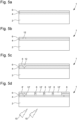
- FIGS. 3a, 3b, 3c, 3d show different steps of a method of producing a photovoltaic cell according to a first variant embodiment.
- a base layer 2 which is a glass layer, and which is part of the photovoltaic cell as such in this case.
- the photovoltaic cell 1 comprises as a base layer, the first front collector layer 4, which is at the end of the production process defined as the front collector.
- the first front collector layer On the first front collector layer, a pi-n type sequence (p-doping, intrinsic i, n-doping) of thin layers of amorphous silicon (a-Si), called absorber or defined as amorphous silicon layer 6, is deposited, and on this amorphous silicon layer 6, a second conductive layer 8 is also added, which is preferably a metal layer such as an aluminum layer.
- the photovoltaic cell 1 can comprise both the glass layer 2 and the three layers specified above or only the three layers specified above.
- the photovoltaic cell 1 can also be mounted or fixed on a dial of the portable object.
- the layer of the front collector 8 which serves directly as a base layer, because at the end of the method of producing the photovoltaic cell 1 of the mono segment type, the latter is mounted or fixed on said dial of the portable object on the side of the second conductive layer (rear collector), which can be a metal layer.
- This first layer of the front collector can advantageously be a layer of zinc oxide ZnO or a layer of zinc oxide doped with aluminum (ZnO:Al or AZO).
- the glass layer 2 is represented as a base layer on which the various other layers of the mono-segment photovoltaic cell 1 are deposited.
- first front collector layer 4 which is weakly electrically conductive. It can be a first front layer 4 which is a zinc oxide ZnO or a first layer of zinc oxide doped with aluminum (ZnO:Al or AZO). Above this first front layer 4, there is provided a pin-type sequence (p-doping, intrinsic i-doping, n-doping) of thin layers of amorphous silicon (a-Si), called an absorber placed or deposited an amorphous silicon layer 6 which is used to capture electromagnetic waves, i.e. light for example in order to convert it into electrical energy through the layers arranged above and below this amorphous silicon layer 6.
- a-Si amorphous silicon
- the general shape of the front layer 4 and of the amorphous silicon layer 6 depends mainly on the general shape of the glass on which they are made or deposited.
- the base layer which is a glass 2 of the portable object, such as a watch
- the first front layer 4 takes a general shape of a circular cylinder so as to be deposited or fixed on an inner face of the watch glass 2.
- the thin layer of amorphous silicon 6 is arranged or deposited on the first front layer 4 and of a shape similar to this first front layer 4.
- the second step of the process shown in the figure 3b consists in making an opening 12 generally in the peripheral position of the photovoltaic cell 1 through the pin type sequence (p-doping, intrinsic i-doping, n-doping) of thin layers of amorphous silicon (a-Si), defined as the layer 6 of amorphous silicon, showing access to the first front layer.
- a-Si amorphous silicon
- Each opening 12 made to connect the first front collector layer can be made by means of a laser or another etching technique as used in microelectronics.
- a second conductive layer 8 is deposited above the amorphous silicon layer 6.
- This second conductive layer 8 is preferably a metal layer, such as an aluminum layer.
- This metal layer, preferably made of aluminum, passes through the opening 12 made in the step of the method seen in figure 3b , to come into contact with the first frontal layer 4.
- the last step of the production process shown in the 3d figure consists in carrying out a separation of the second conductive layer 8, which may be the metal layer for example made of aluminum 8, on the one hand to contact the TCO front layer 4 and on the other hand of the metal layer connected to the parts of at least one negative terminal of the photovoltaic cell.
- an opening 12' is made through the electrically conductive layer 8 in the electrically conductive layer, which may be an aluminum layer 8 and formed in such a way as to separate the metal layer 8' made of aluminum for example connected to the first front layer 4, from the metal layer 8 made of aluminum connected to the negative terminal or terminal of the photovoltaic cell 1.
- beams of light or light 10 can be captured by the photovoltaic cell 1. It will be explained later that the photovoltaic cell 1 is intended to be connected to an electronic module generally located below the dial of the portable object to carry out the conversion of light into electrical energy.
- FIG 4 represents a view from below at the end of the production process to show the separation of the second metal layer, for example made of aluminum, to connect the front collector layer on the one hand and the negative terminal of the photovoltaic cell 1 on the other hand.
- the asymmetric peripheral buses of the present invention namely the positive peripheral bus connected to the front collector layer, and the negative peripheral bus connected to the negative connection terminal of the photovoltaic cell.
- the opening(s) made in the second conductive layer 8, such as the aluminum layer, makes it possible to make the positive peripheral buses 8' for subsequent connection to an electronic module below the dial of the portable object. By making these openings, one can notice the amorphous silicon layer 6 below this conductive layer which is an aluminum layer 8.
- Each positive peripheral bus from the connection with the first front collector layer terminates on a first side with a first positive terminal 8'a and on a second side with a second positive terminal 8'b.
- the two peripheral bus sectors together describe a total circular arc which is defined over at least 330°.
- the negative peripheral bus of the aluminum layer is represented only by the negative terminal 8 which is opposite the two positive terminals 8'a and 8'b.
- the negative peripheral bus is of a circular arc less than 30°, which shows the asymmetry of the positive and negative peripheral buses, which is sought by the present invention.
- the two positive peripheral bus sectors 8' together are approximately 10 times longer than the negative peripheral bus 8 which provides the advantage of the voltage drop reduction mentioned above, particularly at brighter illuminations which produce a greater electrical current.
- the negative terminal 8 is directly connected to the remainder of the metal layer 8 which is without openwork parts and surrounded by the set of two positive peripheral bus sectors 8'.
- FIGS. 5a, 5b, 5c, 5d represent cross-sections of the four steps of the process for producing the photovoltaic cell according to a second variant of production of the photovoltaic cell.
- FIGS 6a, 6b, 6c, 6d represent cross sections of the four stages of the process for producing the photovoltaic cell according to a third variant of production of the photovoltaic cell.
- a chemical etching is carried out to attack both the conductive layer 8, such as a metal layer 8, and the amorphous silicon layer 6 to obtain the openings referenced 12' defining openwork parts.
- a chemical etching is carried out to attack both the conductive layer 8, such as a metal layer 8, and the amorphous silicon layer 6, and also the first front layer 4 above the base layer, which may be the glass 2 of the portable object.
- openwork parts are made to make the photovoltaic cell semi-transparent, it can be planned to have an openwork chosen between 75 and 95%, therefore a maximum of 25% PV coverage, which becomes too visible, and a minimum of 5%, which is difficult to design, because the power of the cell becomes too low.
- the method for producing the photovoltaic cell can start directly with a first front collector layer 4 which constitutes a base layer. From this base layer, the other layers are arranged successively from one face of this first front collector layer 4.
- This first front collector layer 4 can advantageously be made up of a layer of zinc oxide ZnO or first layer of zinc oxide doped with aluminum (ZnO:Al or AZO).
- the photovoltaic cell 1 produced is not combined with a glass of the portable object or directly on the dial of the portable object.
- the photovoltaic cell 1 consisting only of the three aforementioned layers, it must be provided subsequently to be able to connect the connection terminals of the positive peripheral bus and the negative peripheral bus to an electronic module generally arranged below the dial of the portable object so as to manage the signals received via its connection terminals of the positive and negative peripheral buses.
- connection terminals of the positive and negative peripheral buses to the electronic module of the portable object
- ACF film anisotropic conductive film
- a spring rod connector also called pogo
- a Zebra type connector elastic block containing regularly spaced conductive areas
Landscapes
- Photovoltaic Devices (AREA)
Priority Applications (6)
| Application Number | Priority Date | Filing Date | Title |
|---|---|---|---|
| EP23193763.2A EP4517837A1 (de) | 2023-08-28 | 2023-08-28 | Photovoltaische zelle mit spezifischer anordnung von energiekollektoren und verfahren zur herstellung einer solchen zelle |
| US18/782,244 US12563859B2 (en) | 2023-08-28 | 2024-07-24 | Photovoltaic cell with a specific arrangement of energy collectors, and method for producing such a cell |
| JP2024121732A JP7834962B2 (ja) | 2023-08-28 | 2024-07-29 | エネルギー収集体の特定の配列を有する光起電力電池及びかかる電池の製造方法 |
| CN202422092596.4U CN223503312U (zh) | 2023-08-28 | 2024-08-27 | 具有能量收集器的特定布置的光伏电芯 |
| CN202411182532.1A CN119562649A (zh) | 2023-08-28 | 2024-08-27 | 具有能量收集器的特定布置的光伏电芯以及用于生产这种电芯的方法 |
| KR1020240116130A KR20250033056A (ko) | 2023-08-28 | 2024-08-28 | 에너지 컬렉터들의 특정 배열을 갖는 광기전 전지 및 그러한 전지를 제조하기 위한 방법 |
Applications Claiming Priority (1)
| Application Number | Priority Date | Filing Date | Title |
|---|---|---|---|
| EP23193763.2A EP4517837A1 (de) | 2023-08-28 | 2023-08-28 | Photovoltaische zelle mit spezifischer anordnung von energiekollektoren und verfahren zur herstellung einer solchen zelle |
Publications (1)
| Publication Number | Publication Date |
|---|---|
| EP4517837A1 true EP4517837A1 (de) | 2025-03-05 |
Family
ID=87848104
Family Applications (1)
| Application Number | Title | Priority Date | Filing Date |
|---|---|---|---|
| EP23193763.2A Pending EP4517837A1 (de) | 2023-08-28 | 2023-08-28 | Photovoltaische zelle mit spezifischer anordnung von energiekollektoren und verfahren zur herstellung einer solchen zelle |
Country Status (5)
| Country | Link |
|---|---|
| US (1) | US12563859B2 (de) |
| EP (1) | EP4517837A1 (de) |
| JP (1) | JP7834962B2 (de) |
| KR (1) | KR20250033056A (de) |
| CN (2) | CN119562649A (de) |
Citations (5)
| Publication number | Priority date | Publication date | Assignee | Title |
|---|---|---|---|---|
| WO1998004005A1 (fr) * | 1996-07-24 | 1998-01-29 | Tdk Corporation | Batterie photovoltaique |
| EP1045454A1 (de) * | 1998-07-27 | 2000-10-18 | Citizen Watch Co., Ltd. | Solarzelle und herstellungsverfahren, und maske für photolithographie zur herstellung der solarzelle |
| US20020050286A1 (en) * | 1998-03-25 | 2002-05-02 | Tdk Corporation | Solar battery module |
| WO2023030703A1 (fr) * | 2021-08-30 | 2023-03-09 | The Swatch Group Research And Development Ltd | Appareil électronique comprenant une cellule solaire et procédé de fabrication de ladite cellule solaire |
| CH718934A2 (fr) * | 2021-08-30 | 2023-03-15 | Swatch Group Res & Dev Ltd | Cellule solaire, pièce d'horlogerie comprenant ladite cellule solaire et procédé de fabrication de ladite cellule solaire. |
Family Cites Families (8)
| Publication number | Priority date | Publication date | Assignee | Title |
|---|---|---|---|---|
| JPS6286876A (ja) * | 1985-10-14 | 1987-04-21 | Fuji Electric Co Ltd | 時計用太陽電池 |
| JP2951146B2 (ja) | 1992-04-15 | 1999-09-20 | キヤノン株式会社 | 光起電力デバイス |
| JP3467424B2 (ja) * | 1998-03-25 | 2003-11-17 | Tdk株式会社 | 太陽電池モジュール |
| WO2000028513A1 (fr) * | 1998-11-10 | 2000-05-18 | Citizen Watch Co., Ltd. | Dispositif electronique comportant une cellule solaire |
| WO2000031596A1 (en) * | 1998-11-26 | 2000-06-02 | Citizen Watch Co., Ltd. | Timepiece |
| EP1186966B1 (de) * | 2000-03-21 | 2018-08-08 | Citizen Watch Co., Ltd. | Elektronische einheit |
| CN110176506B (zh) * | 2019-05-31 | 2024-05-07 | 信利半导体有限公司 | 薄膜光伏电池串联结构及薄膜光伏电池串联的制备工艺 |
| CN113917723B (zh) | 2021-09-30 | 2024-04-09 | 信利半导体有限公司 | 一种集成光感应器和太阳能电池的显示屏及其制备方法 |
-
2023
- 2023-08-28 EP EP23193763.2A patent/EP4517837A1/de active Pending
-
2024
- 2024-07-24 US US18/782,244 patent/US12563859B2/en active Active
- 2024-07-29 JP JP2024121732A patent/JP7834962B2/ja active Active
- 2024-08-27 CN CN202411182532.1A patent/CN119562649A/zh active Pending
- 2024-08-27 CN CN202422092596.4U patent/CN223503312U/zh active Active
- 2024-08-28 KR KR1020240116130A patent/KR20250033056A/ko active Pending
Patent Citations (5)
| Publication number | Priority date | Publication date | Assignee | Title |
|---|---|---|---|---|
| WO1998004005A1 (fr) * | 1996-07-24 | 1998-01-29 | Tdk Corporation | Batterie photovoltaique |
| US20020050286A1 (en) * | 1998-03-25 | 2002-05-02 | Tdk Corporation | Solar battery module |
| EP1045454A1 (de) * | 1998-07-27 | 2000-10-18 | Citizen Watch Co., Ltd. | Solarzelle und herstellungsverfahren, und maske für photolithographie zur herstellung der solarzelle |
| WO2023030703A1 (fr) * | 2021-08-30 | 2023-03-09 | The Swatch Group Research And Development Ltd | Appareil électronique comprenant une cellule solaire et procédé de fabrication de ladite cellule solaire |
| CH718934A2 (fr) * | 2021-08-30 | 2023-03-15 | Swatch Group Res & Dev Ltd | Cellule solaire, pièce d'horlogerie comprenant ladite cellule solaire et procédé de fabrication de ladite cellule solaire. |
Also Published As
| Publication number | Publication date |
|---|---|
| US12563859B2 (en) | 2026-02-24 |
| CN223503312U (zh) | 2025-10-31 |
| US20250081663A1 (en) | 2025-03-06 |
| KR20250033056A (ko) | 2025-03-07 |
| CN119562649A (zh) | 2025-03-04 |
| JP7834962B2 (ja) | 2026-03-25 |
| JP2025032972A (ja) | 2025-03-12 |
Similar Documents
| Publication | Publication Date | Title |
|---|---|---|
| EP3000131B1 (de) | Halbtransparente fotovoltaische dünnschichtmonozelle | |
| EP2339647B1 (de) | Photodetektor mit Plasmonstruktur | |
| EP2752893B1 (de) | Halbleiterstruktur vom Typ Lawinen-Fotodiode, und Herstellungsverfahren einer solchen Struktur | |
| WO2013105031A2 (fr) | Procede pour realiser un module photovoltaïque avec deux etapes de gravure p2 et p3 et module photovoltaïque correspondant | |
| FR2954854A1 (fr) | Photodetecteur a structure plasmon | |
| EP2477231A2 (de) | Fotodetektor, der durch eine Metallstrukturierung mit Anordnung auf der Rückseite optimiert ist | |
| EP2786426B1 (de) | Halbleiterstruktur zur aufnahme von elektromagnetischer strahlung, halbleiterbauelement und verfahren zur herstellung einer solchen halbleiterstruktur | |
| FR2961022A1 (fr) | Cellule photovoltaïque pour application sous flux solaire concentre | |
| FR3083369A1 (fr) | Interconnexion monolithique de modules photovoltaiques | |
| WO2013105024A1 (fr) | Procede pour realiser un module photovoltaïque avec deux etapes de gravure p1 et p3 et module photovoltaïque correspondant | |
| EP4517837A1 (de) | Photovoltaische zelle mit spezifischer anordnung von energiekollektoren und verfahren zur herstellung einer solchen zelle | |
| CH721083A2 (fr) | Cellule photovoltaïque avec collecteurs d'énergie asymétriques, et procédé de réalisation d'une telle cellule | |
| FR2985604A1 (fr) | Dispositif de photodetection. | |
| FR2989223A1 (fr) | Procede pour realiser un module photovoltaique avec une etape de gravure p3 et une eventuelle etape p1. | |
| EP2842170B1 (de) | Verfahren zur herstellung eines strukturierten reflektors für eine photovoltaische dünnschichtzelle und entsprechender strukturierter reflektor | |
| FR3073981A1 (fr) | Module photovoltaique multi-cellules semi-transparent soumis a ombrage peripherique recurrent | |
| EP4264679B1 (de) | Herstellungsverfahren von mindestens einer photovoltaïschen zelle mit einem von mindestens einem draht unterstützten wafer | |
| FR3018392A1 (fr) | Module solaire photovoltaique semi-transparent en couches minces et son procede de fabrication | |
| EP4199122A1 (de) | Photovoltaische zelle mit passiven kontakten und antireflexionsbeschichtung | |
| WO2024115696A1 (fr) | Ensemble pour module photovoltaïque, module photovoltaïque et procédé de fabrication de l'ensemble et du module | |
| FR2989224A1 (fr) | Procede pour realiser un module photovoltaique avec une etape de gravure p3 et une eventuelle etape p2. | |
| FR3023062A1 (fr) | Cellule photovoltaique a heterojonction de silicium et procede de fabrication d'une telle cellule | |
| FR2947954A1 (fr) | Cellule texturee a rendement de conversion eleve comportant une zone texturee recouverte par une bi-couche antireflet | |
| WO2020229880A1 (fr) | Module photovoltaïque multi-cellules semi-transparent soumis a ombrage peripherique recurrent | |
| FR3086458A1 (fr) | Dispositif photovoltaique semi-transparent avec une grille de collecte du courant electrique optimisee |
Legal Events
| Date | Code | Title | Description |
|---|---|---|---|
| PUAI | Public reference made under article 153(3) epc to a published international application that has entered the european phase |
Free format text: ORIGINAL CODE: 0009012 |
|
| STAA | Information on the status of an ep patent application or granted ep patent |
Free format text: STATUS: THE APPLICATION HAS BEEN PUBLISHED |
|
| AK | Designated contracting states |
Kind code of ref document: A1 Designated state(s): AL AT BE BG CH CY CZ DE DK EE ES FI FR GB GR HR HU IE IS IT LI LT LU LV MC ME MK MT NL NO PL PT RO RS SE SI SK SM TR |
|
| P01 | Opt-out of the competence of the unified patent court (upc) registered |
Free format text: CASE NUMBER: APP_29215/2025 Effective date: 20250618 |
|
| STAA | Information on the status of an ep patent application or granted ep patent |
Free format text: STATUS: REQUEST FOR EXAMINATION WAS MADE |
|
| 17P | Request for examination filed |
Effective date: 20250822 |