EP4518078A1 - Vorrichtung zur steuerung von fotovoltaischen komponenten - Google Patents
Vorrichtung zur steuerung von fotovoltaischen komponenten Download PDFInfo
- Publication number
- EP4518078A1 EP4518078A1 EP24167940.6A EP24167940A EP4518078A1 EP 4518078 A1 EP4518078 A1 EP 4518078A1 EP 24167940 A EP24167940 A EP 24167940A EP 4518078 A1 EP4518078 A1 EP 4518078A1
- Authority
- EP
- European Patent Office
- Prior art keywords
- photovoltaic component
- bypass
- voltage
- module
- photovoltaic
- Prior art date
- Legal status (The legal status is an assumption and is not a legal conclusion. Google has not performed a legal analysis and makes no representation as to the accuracy of the status listed.)
- Pending
Links
Images





Classifications
-
- H—ELECTRICITY
- H02—GENERATION; CONVERSION OR DISTRIBUTION OF ELECTRIC POWER
- H02J—ELECTRIC POWER NETWORKS; CIRCUIT ARRANGEMENTS OR SYSTEMS FOR SUPPLYING OR DISTRIBUTING ELECTRIC POWER; SYSTEMS FOR STORING ELECTRIC ENERGY
- H02J3/00—Circuit arrangements for AC mains or AC distribution networks
- H02J3/38—Arrangements for feeding a single network from two or more generators or sources in parallel; Arrangements for feeding already energised networks from additional generators or sources in parallel
- H02J3/46—Controlling the sharing of generated power between the generators, sources or networks
-
- H—ELECTRICITY
- H02—GENERATION; CONVERSION OR DISTRIBUTION OF ELECTRIC POWER
- H02J—ELECTRIC POWER NETWORKS; CIRCUIT ARRANGEMENTS OR SYSTEMS FOR SUPPLYING OR DISTRIBUTING ELECTRIC POWER; SYSTEMS FOR STORING ELECTRIC ENERGY
- H02J3/00—Circuit arrangements for AC mains or AC distribution networks
- H02J3/38—Arrangements for feeding a single network from two or more generators or sources in parallel; Arrangements for feeding already energised networks from additional generators or sources in parallel
- H02J3/381—Dispersed generators
-
- H—ELECTRICITY
- H02—GENERATION; CONVERSION OR DISTRIBUTION OF ELECTRIC POWER
- H02J—ELECTRIC POWER NETWORKS; CIRCUIT ARRANGEMENTS OR SYSTEMS FOR SUPPLYING OR DISTRIBUTING ELECTRIC POWER; SYSTEMS FOR STORING ELECTRIC ENERGY
- H02J3/00—Circuit arrangements for AC mains or AC distribution networks
- H02J3/007—Arrangements for selectively connecting one or more loads to one or more power sources or power lines
-
- H—ELECTRICITY
- H02—GENERATION; CONVERSION OR DISTRIBUTION OF ELECTRIC POWER
- H02J—ELECTRIC POWER NETWORKS; CIRCUIT ARRANGEMENTS OR SYSTEMS FOR SUPPLYING OR DISTRIBUTING ELECTRIC POWER; SYSTEMS FOR STORING ELECTRIC ENERGY
- H02J7/00—Circuit arrangements for charging or discharging batteries or for supplying loads from batteries
- H02J7/34—Parallel operation in networks using both storage and other DC sources, e.g. providing buffering
- H02J7/35—Parallel operation in networks using both storage and other DC sources, e.g. providing buffering with light sensitive cells
-
- H—ELECTRICITY
- H02—GENERATION; CONVERSION OR DISTRIBUTION OF ELECTRIC POWER
- H02M—APPARATUS FOR CONVERSION BETWEEN AC AND AC, BETWEEN AC AND DC, OR BETWEEN DC AND DC, AND FOR USE WITH MAINS OR SIMILAR POWER SUPPLY SYSTEMS; CONVERSION OF DC OR AC INPUT POWER INTO SURGE OUTPUT POWER; CONTROL OR REGULATION THEREOF
- H02M1/00—Details of apparatus for conversion
- H02M1/08—Circuits specially adapted for the generation of control voltages for semiconductor devices incorporated in static converters
-
- H—ELECTRICITY
- H02—GENERATION; CONVERSION OR DISTRIBUTION OF ELECTRIC POWER
- H02M—APPARATUS FOR CONVERSION BETWEEN AC AND AC, BETWEEN AC AND DC, OR BETWEEN DC AND DC, AND FOR USE WITH MAINS OR SIMILAR POWER SUPPLY SYSTEMS; CONVERSION OF DC OR AC INPUT POWER INTO SURGE OUTPUT POWER; CONTROL OR REGULATION THEREOF
- H02M3/00—Conversion of DC power input into DC power output
- H02M3/02—Conversion of DC power input into DC power output without intermediate conversion into AC
- H02M3/04—Conversion of DC power input into DC power output without intermediate conversion into AC by static converters
- H02M3/10—Conversion of DC power input into DC power output without intermediate conversion into AC by static converters using discharge tubes with control electrode or semiconductor devices with control electrode
- H02M3/145—Conversion of DC power input into DC power output without intermediate conversion into AC by static converters using discharge tubes with control electrode or semiconductor devices with control electrode using devices of a triode or transistor type requiring continuous application of a control signal
- H02M3/155—Conversion of DC power input into DC power output without intermediate conversion into AC by static converters using discharge tubes with control electrode or semiconductor devices with control electrode using devices of a triode or transistor type requiring continuous application of a control signal using semiconductor devices only
- H02M3/156—Conversion of DC power input into DC power output without intermediate conversion into AC by static converters using discharge tubes with control electrode or semiconductor devices with control electrode using devices of a triode or transistor type requiring continuous application of a control signal using semiconductor devices only with automatic control of output voltage or current, e.g. switching regulators
-
- H—ELECTRICITY
- H02—GENERATION; CONVERSION OR DISTRIBUTION OF ELECTRIC POWER
- H02S—GENERATION OF ELECTRIC POWER BY CONVERSION OF INFRARED RADIATION, VISIBLE LIGHT OR ULTRAVIOLET LIGHT, e.g. USING PHOTOVOLTAIC [PV] MODULES
- H02S40/00—Components or accessories in combination with PV modules, not provided for in groups H02S10/00 - H02S30/00
- H02S40/30—Electrical components
-
- H—ELECTRICITY
- H02—GENERATION; CONVERSION OR DISTRIBUTION OF ELECTRIC POWER
- H02S—GENERATION OF ELECTRIC POWER BY CONVERSION OF INFRARED RADIATION, VISIBLE LIGHT OR ULTRAVIOLET LIGHT, e.g. USING PHOTOVOLTAIC [PV] MODULES
- H02S40/00—Components or accessories in combination with PV modules, not provided for in groups H02S10/00 - H02S30/00
- H02S40/30—Electrical components
- H02S40/34—Electrical components comprising specially adapted electrical connection means to be structurally associated with the PV module, e.g. junction boxes
-
- H—ELECTRICITY
- H02—GENERATION; CONVERSION OR DISTRIBUTION OF ELECTRIC POWER
- H02S—GENERATION OF ELECTRIC POWER BY CONVERSION OF INFRARED RADIATION, VISIBLE LIGHT OR ULTRAVIOLET LIGHT, e.g. USING PHOTOVOLTAIC [PV] MODULES
- H02S50/00—Monitoring or testing of PV systems, e.g. load balancing or fault identification
-
- H—ELECTRICITY
- H02—GENERATION; CONVERSION OR DISTRIBUTION OF ELECTRIC POWER
- H02S—GENERATION OF ELECTRIC POWER BY CONVERSION OF INFRARED RADIATION, VISIBLE LIGHT OR ULTRAVIOLET LIGHT, e.g. USING PHOTOVOLTAIC [PV] MODULES
- H02S50/00—Monitoring or testing of PV systems, e.g. load balancing or fault identification
- H02S50/10—Testing of PV devices, e.g. of PV modules or single PV cells
-
- H—ELECTRICITY
- H10—SEMICONDUCTOR DEVICES; ELECTRIC SOLID-STATE DEVICES NOT OTHERWISE PROVIDED FOR
- H10F—INORGANIC SEMICONDUCTOR DEVICES SENSITIVE TO INFRARED RADIATION, LIGHT, ELECTROMAGNETIC RADIATION OF SHORTER WAVELENGTH OR CORPUSCULAR RADIATION
- H10F77/00—Constructional details of devices covered by this subclass
- H10F77/95—Circuit arrangements
- H10F77/953—Circuit arrangements for devices having potential barriers
- H10F77/955—Circuit arrangements for devices having potential barriers for photovoltaic devices
-
- H—ELECTRICITY
- H02—GENERATION; CONVERSION OR DISTRIBUTION OF ELECTRIC POWER
- H02J—ELECTRIC POWER NETWORKS; CIRCUIT ARRANGEMENTS OR SYSTEMS FOR SUPPLYING OR DISTRIBUTING ELECTRIC POWER; SYSTEMS FOR STORING ELECTRIC ENERGY
- H02J2101/00—Supply or distribution of decentralised, dispersed or local electric power generation
- H02J2101/20—Dispersed power generation using renewable energy sources
- H02J2101/22—Solar energy
- H02J2101/24—Photovoltaics
-
- Y—GENERAL TAGGING OF NEW TECHNOLOGICAL DEVELOPMENTS; GENERAL TAGGING OF CROSS-SECTIONAL TECHNOLOGIES SPANNING OVER SEVERAL SECTIONS OF THE IPC; TECHNICAL SUBJECTS COVERED BY FORMER USPC CROSS-REFERENCE ART COLLECTIONS [XRACs] AND DIGESTS
- Y02—TECHNOLOGIES OR APPLICATIONS FOR MITIGATION OR ADAPTATION AGAINST CLIMATE CHANGE
- Y02E—REDUCTION OF GREENHOUSE GAS [GHG] EMISSIONS, RELATED TO ENERGY GENERATION, TRANSMISSION OR DISTRIBUTION
- Y02E10/00—Energy generation through renewable energy sources
- Y02E10/50—Photovoltaic [PV] energy
Definitions
- the present disclosure relates to the field of photovoltaic technology, and in particular, to a photovoltaic component control device.
- the photovoltaic inverter grid-connected power system consists of a photovoltaic array and an inverter system.
- the photovoltaic array is composed of a plurality of photovoltaic components connected in series and provides sufficient and stable energy for the photovoltaic system.
- the photovoltaic component is the smallest indivisible photovoltaic cell combination device that is packaged and capable of providing direct current output individually. It is also referred to as a solar module or a solar panel.
- the photovoltaic component is composed of a plurality of cell units and reverse protection diodes connected to the cell units in parallel. A rapid control device is a common protection mechanism in the photovoltaic system.
- a traditional control device is a series-type control device, that is, there are switch transistors connected in series in a voltage output circuit of the photovoltaic component.
- the switch transistors When the photovoltaic system generates power normally, the switch transistors are connected in series in a constant ON state to ensure the series connection of the modules and normal operation of the photovoltaic system.
- the switch transistors connected in series and photovoltaic arrays connected in series are disconnected, so that voltage at any interface of the array meets the safety rules, thereby protecting the safety of the inverter system.
- the above-mentioned series-type control device has major defects.
- the switch transistors connected in series are in a constant ON state, a large amount of energy consumption may be generated by the keeping-on switch transistors, resulting in low power generation efficiency.
- embodiments of the present disclosure provide a photovoltaic component control device to solve at least one of the problems existed in the background.
- an embodiment of the present disclosure provides a photovoltaic component control device, including at least one bypass module, a driving circuit, a power supply module, and a controller.
- the at least one bypass module is configured to connect in parallel to at least one photovoltaic component.
- the power supply module is configured to connect to the at least one photovoltaic component and the at least one bypass module.
- the at least one bypass module is configured to bypass the at least one photovoltaic component under control of the controller.
- the driving circuit is configured to drive the at least one bypass module to operate under the control of the controller.
- the power supply module is configured to obtain energy from the at least one photovoltaic component and output the energy to the controller.
- the controller is configured to control an ON state of the at least one bypass module to control whether the at least one photovoltaic component is in a bypass mode.
- the at least one bypass module may include a power switch device.
- An input end and an output end of the power switch device may be respectively connected to a positive electrode and a negative electrode of the at least one photovoltaic component.
- a control end of the power switch device may be configured to receive a driving signal of the driving circuit.
- the at least one bypass module may include a reverse current protection unit connected in series to the power switch device and configured to prevent the power switch device from being damaged by reverse current.
- the at least one bypass module may include a voltage drop adjustment unit configured to adjust a voltage drop between an input end and an output end of the at least one bypass module to a predetermined value in a case that the power switch device is in an operation state.
- the at least one bypass module may include at least one diode, and the at least one diode may be connected in series to the power switch device.
- the power supply module may include a buck circuit configured to convert a voltage output by the at least one photovoltaic component to a second operating voltage in a case that the at least one photovoltaic component operates normally.
- the power supply module may include a boost circuit configured to convert a voltage between the input end and the output end of the at least one bypass module to a first operating voltage in a case that the at least one photovoltaic component is bypassed.
- the power supply module may include a switching circuit configured to compare the second operating voltage with a reference voltage, and control whether the boost circuit and the at least one bypass module may be turned on or off according to the comparison result.
- the switching circuit may include a comparator and at least one switch transistor, a first signal input end of the comparator may be configured to receive the second operating voltage output by the buck circuit, and a second signal input end of the comparator may be configured to receive a reference signal, an input end and an output end of the at least one switch transistor may be connected to the boost circuit and the bypass module, and a control end of the at least one switch transistor may be connected to a signal output end of the comparator.
- the at least one bypass module may include two or more bypass modules connected in series, and the two or more bypass modules connected in series may be configured to connect in parallel to the at least one photovoltaic component.
- the controller may include a communication module, a voltage detection circuit, and/or a temperature detection circuit.
- the communication module may be configured to receive a control signal and transmit the control signal to the controller.
- connection in the context of the present disclosure means transmission of an electrical signal or data between one connected end and another end connected to the one connected end, which can be understood as “electrical connection”, “communication connection”, etc.
- a is directly connected to B means that there are no other elements other than a wire between A and B.
- a switch S2 may be connected in series to a voltage output circuit of a photovoltaic component 2, and a voltage output end of the photovoltaic component 2 after being connected in series to the switch S2 may be connected in parallel to an anti-reverse diode D2.
- a switch Sn may be connected in series to a voltage output circuit of a photovoltaic component n, and a voltage output end of the photovoltaic component n after being connected in series to the switch Sn may be connected in parallel to an anti-reverse diode Dn.
- the voltage output circuit of the photovoltaic component 1 may be connected to a power supply circuit which is configured to supply energy to a control circuit so that the control circuit can operate continually.
- the inventor found that the above-mentioned series-type control device may have the following defects. Firstly, when the photovoltaic component operates normally, the series-type switch transistors may be in a constant turn-on state, and the ON switch transistors may consume a large amount of energy. Secondly, the series-type control device has high requirements on an OFF logic and timing control, the complexity of the control system causes high cost of the control device. Thirdly, when a first switch transistor in the control device is disconnected, the first switch transistor must withstand high voltage stress of a photovoltaic component system, and a risk of overvoltage breakdown exists.
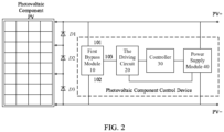
- an embodiment of the present disclosure provides a photovoltaic component control device including at least one first bypass module 10, a driving circuit 20, a power supply module 40, and a controller 30.
- the at least one bypass module is configured to connect in parallel to at least one photovoltaic component and bypass the at least one photovoltaic component under the control of the controller 30.
- the at least one photovoltaic component may be in a bypass mode.
- the at least one bypass module may be one bypass module or more than two bypass modules.
- the at least one photovoltaic component may be one photovoltaic component or more than two photovoltaic components.
- the first bypass module 10 may be configured to connect in parallel to a photovoltaic component PV1. That is, a voltage input end 101 and a voltage output end 102 of the first bypass module 10 may be respectively connected to a positive electrode and a negative electrode of PV1. A switch device may be not included between the voltage input end 101 and the positive electrode of the at least one photovoltaic component PV1 and between the voltage output end 102 and the negative electrode of PV1. A control end 103 of the first bypass module 10 may be connected to a driving circuit 20 and configured to receive a driving signal output by the driving circuit 20.
- the first bypass module 10 may include a power switch device.
- the power switch device may include a relay, a thyristor, a MOSFET, an IGBT, or the like.
- the driving circuit 20 receives a control signal from the controller 30 and outputs a driving voltage to the at least one bypass module 10, which will drive the at least one bypass module 10 to operate under the control of the controller 30.
- the driving circuit 20 may also obtain operating voltage from the power supply module 40.
- the controller 30 is configured to control the ON state of the at least one bypass module 10 to control whether the at least one photovoltaic component is in the bypass mode.
- the controller 30 may output the control signal to the driving circuit 20, and the driving circuit 20 may further drive the first bypass module 10 to turn on to bypass the at least one photovoltaic component PV1 so that the at least one photovoltaic component PV1 is in the bypass mode and stop outputting power to outside.
- An occasion that the at least one photovoltaic component PV1 needs to be bypassed may include the failure of a power system or a safety incident, such as direct current arcing of the photovoltaic component, the failure of a photovoltaic component, fire, etc.
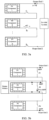
- FIG. 3a is a schematic diagram illustrating a state when a photovoltaic component is turned off by a traditional series-type turn-off device.
- FIG. 3b is a schematic diagram illustrating a bypass mode of a single component according to an embodiment of the present disclosure, in which the bypass module may be equivalent to a switch.
- FIG. 3c is a schematic diagram illustrating a bypass mode of whole components according to an embodiment of the present disclosure, in which the bypass module may be equivalent to a switch.
- switches S 1 ⁇ S n may be closed and the bypass module may be turned on.
- At least one bypass module may include n bypass modules including a first bypass module 10, a second bypass module 20, ..., and an n th bypass module n10.
- At least one photovoltaic component may include n photovoltaic components including a first photovoltaic component PV1, a second photovoltaic component PV2, ..., an n th photovoltaic component PVn, where, n represents a natural number greater than one.
- each bypass module may be driven by a corresponding driving circuit, or different bypass modules may be driven by a same driving circuit.
- the at least one photovoltaic component includes two or more photovoltaic components, the two or more photovoltaic components can be connected in series or parallel.
- each bypass module may be connected in parallel to a photovoltaic component, so that a failure component can be independently removed without affecting the normal operation of other components, thereby achieving rapidly turning off a single component.
- a first bypass module 10 may be connected in parallel to a first photovoltaic component PV1
- an n th bypass module n10 may be connected in parallel to an n th photovoltaic component PVn.
- the n th bypass module n10 may be driven by a driving circuit n20.
- the controller 30 can control whether a plurality of bypass modules are turned on or off at the same time, thereby realizing rapidly turning off a single component.
- a bypass module may be connected in parallel to more than two photovoltaic components, and more than two photovoltaic components can be turned off at the same time, thereby realizing the rapidly turning off a plurality of components.
- the first bypass module 10 is connected in parallel to the first photovoltaic component PV1
- the n th bypass module n10 is connected in parallel to more than two photovoltaic components.
- the first bypass module 10 may be connected in parallel to more than two photovoltaic components, and the n th bypass module n10 may be also connected in parallel to more than two photovoltaic components.
- the power supply module 40 may obtain energy from a certain photovoltaic component and provide the energy to the controller 30 and other modules.
- the controller 30 can control the bypass protection mechanism of the plurality of photovoltaic components, thereby reducing cost.
- the control device in the embodiment of the present disclosure may be a pure bypass-type control device, and in a bypass module connected in parallel to the photovoltaic component, a switch device may be not disposed between the voltage input end 101 and the positive electrode of the photovoltaic component, and between the voltage output end 102 and the negative electrode of the photovoltaic component.
- the controller 30 may control at least one bypass module to be disconnected, and the photovoltaic component may output energy to outside.
- the power supply module 40 may obtain the energy from the photovoltaic component and supply the energy to the controller.
- the controller 30 may control at least one bypass module to be turned on.
- the photovoltaic component connected in parallel to the at least one bypass module may be protected by a bypass short circuit.
- the photovoltaic component may form a discharge circuit with the at least one bypass module, but not output energy to outside.
- the photovoltaic component has no safety hazard caused by turning on in series connection and meets the safety rules, thereby ensuring the power safety of the photovoltaic system.
- the power supply module 40 may obtain energy from the bypassed photovoltaic component and continuously supply the energy to the controller 30 and the driving circuit 20.
- the pure bypass-type control device is adopted in the embodiment of the present disclosure, that is, the bypass module is directly connected in parallel with the photovoltaic component and no switch device is connected in series between the photovoltaic component and the bypass module, thus completely avoiding energy consumption generated by the constant ON of a series-type switch transistor in a series-type turn-off device, reducing the power consumption, and improving the output power of the photovoltaic array.
- the problem of voltage stress on the first series-type switch transistor in the series-type turn-off device when it is disconnected is solved, and the safety performance is improved.
- the elimination of the series-type switch transistor may simplify the circuit structure of the control device, reduce the complex turn-off logic and timing control requirement, improve the reliability of the control device, and reduce the cost.
- the bypass-type rapid control device for the photovoltaic component in the embodiment of the present disclosure can be applied to photovoltaic arrays with different sizes.
- the bypass protection mechanism can eliminate keeping-on restriction between series-connected photovoltaic components and can maximize the power generation of the photovoltaic arrays.
- the power supply module provided in the embodiment of the present disclosure can directly obtain energy from the photovoltaic component under the normal operation state and the bypass state, thereby ensuring the reliability of the power supply of the control device, improving the reliability of the control device and the efficiency of the photovoltaic component system, and reducing cost.
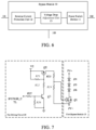
- At least one bypass module 10 may include a power switch device 11, a reverse current protection unit 12, and a voltage drop adjustment unit 13. Input and output ends of the power switch device11 may be connected to positive and negative electrodes of a photovoltaic component, respectively. A control end 103 of the power switch device 11 may be configured to receive a driving signal of the driving circuit 20. The driving circuit 20 may be controlled by the controller 30. The power switch device 11 bypasses the photovoltaic component under the control of the controller 30.
- the reverse current protection unit 12 may be configured to prevent the power switch device 11 from being damaged by reverse current.
- the voltage drop adjustment unit 13 may be configured to adjust a voltage drop between the input end and the output end of the bypass module in which it is located to a predetermined value in the case that the power switch device 11 is in an operation state (ON). In the case that the photovoltaic component is bypassed and the bypass module is in the operation state, the voltage drop adjustment unit 13 may provide operating voltage to the power supply module 40 to ensure the normal operation thereof.
- the first bypass module 10 may include a first MOS transistor Q1 and at least one diode connected in series with Q1.
- FIG. 7 illustrates a case that three series-connected diodes D4, D5, and D6 are adopted.
- the NMOS transistor Q1 may be served as the power switch device 11.
- the three series-connected diodes D4, D5, and D6 may be served as the reverse current protection unit 12 and the voltage drop adjustment unit 13 at the same time.
- Positive and negative output ends of the photovoltaic component may be connected to the bypass module.
- An end of the positive electrode PV+ of the photovoltaic component may be connected to the three series-connected diodes D4, D5, and D6, and then connected in series to the power switch transistor Q1.
- the switch transistor may be connected to an end of the component to form a controllable unidirectional bypass short-circuit protection circuit.
- An anode of D4 may be connected to the positive electrode PV+ of the photovoltaic component, a cathode of D4 may be connected to an anode of D5, and a cathode of D5 may be connected to an anode of D6.
- a cathode of D6 may be connected to a drain of Q1.
- a source of Q1 may be connected to a negative electrode PV- of the photovoltaic component.
- a gate of Q1 may be connected to a driving signal output end of the driving circuit 20.
- FIGs. 5a and 5b when a first photovoltaic component PV1 connected in parallel to the first bypass module 10 is connected in series to other photovoltaic components, if PV1 is short-circuited by the first bypass module 10, the current output by the other photovoltaic components will flow through the first bypass module 10 in a reverse direction and cause damage to a body diode of Q 1.
- the diodes connected in series may include the voltage drop adjustment unit 13, and provide operating voltage for the power supply module 40 to ensure the normal operation thereof in the case that the first bypass module 10 is operating.
- the number of the at least one diode is not limited to three, and can be determined according to the reverse current it can withstand and the operating voltage required by the power supply module 40.
- the at least one diode may cause a voltage drop of more than 0.9V between the input end 101 and the output end 102 of the first bypass module 10.
- the power switch device 11 can also be replaced by another power switch device, such as a relay, an IGBT, etc.
- Q1 is not limited to the NMOS transistor shown in FIG. 7 , but can also be a PMOS transistor.
- the voltage drop adjustment unit 13 may also be a resistor, which may be connected in series to the at least one diode (not shown in the figure).
- the driving circuit 20 may include a second MOS transistor Q2 and a third triode Q3.
- Q2 may be a P-channel MOS transistor, and Q3 may be an N-type triode.
- a source of Q2 may be connected to a second voltage input end V2.
- a first resistor R21 may be connected between a gate and the source of Q2.
- the gate of Q2 may be connected to a base of Q3 through a second resistor R22.
- R21 and R22 are voltage dividing resistors.
- a drain of Q2 may be connected to a negative electrode of the photovoltaic component through the third resistor R23 and the fourth resistor R24.
- the drain of Q2 may be connected to the gate of Q1 through the third resistor R23.
- R18 represents a driving signal input resistor of the first bypass module 10.
- R23 represents the base of Q3 and may receive the control signal BYPASS_CTL of the controller 30 through a fifth resistor R25.
- a sixth resistor R26 may be connected between the base and an emitter of Q3.
- R24 and R26 represent charge and discharge resistors. The emitter of Q3 must be connected to the ground.
- the driving circuit 20 may obtain the second voltage V2 from the power supply module, for example, the voltage of 5V provides conduction voltage to Q1.
- the controller 30 may output the control signal BYPASS_CTL to control Q3 to be turned on or off.
- BYPASS_CTL When BYPASS_CTL is at a high potential, Q3 is turned on, a potential between R21 and R22 is lower than 5V, Q2 is turned on, R23 and R34 generate a high potential, Q1 is turned on, and the first bypass module 10 is turned on.
- BYPASS_CTL is at a low potential, Q3 is cut off, the potential between R21 and R22 is equal to 5V, Q2 is cut off, R23 and R24 are at a low potential, Q1 is cut off, and the bypass module must be disconnected.
- the power supply module 40 may include a buck circuit 41 configured to convert a voltage output by at least one photovoltaic component to a second operating voltage in the case that at least one photovoltaic component operates normally; a boost circuit 42 configured to convert a voltage between the input end and the output end of the at least one bypass module into a first operating voltage in the case that at least one photovoltaic component is bypassed; a switching circuit 43 configured to compare the second operating voltage with a reference voltage, and control whether the boost circuit and at least one bypass module are turned on according to a comparison result.
- the reference voltage may be the control voltage BYPASS_CTL output by the controller 30.
- the pin 413 may be connected to the ground through the first inductor L1 and the third capacitor C3 which are connected in series.
- the first inductor L1 and the third capacitor C3 may form an LC filter structure to filter out a high-frequency harmonics and stabilize the output DC voltage (a second voltage V2).
- An output end of the second voltage V2 may be connected to the ground through series-connected ninth resistor R414 and tenth resistor R413.
- the pin 416 may be connected between R414 and R413 and used to sample the output voltage V2 and form a feedback signal to the chip U1.
- R421 represents an enable input resistor, which may control an input size of the enable signal.
- the pin 425 may be connected to the ground.
- the pin 422 may be a voltage output end and connected to the ground through a sixth capacitor C6. C6 may be used to filter out an interference waveform and stabilize DC output.
- the pin 422 may be also connected to the ground through series-connected fourteenth resistor R423 and thirteenth resistor R422.
- the pin 426 may be connected between R423 and R422, and used to sample an output voltage and form a feedback signal to the chip U2. To stabilize the first voltage V1 output by the boost circuit 42, the voltage output pin 422 of U2 may be connected to a twelfth transistor D10 to obtain the stable first voltage V1.
- the switching circuit 43 may include a comparator and at least one switch transistor.
- a first signal input end of the comparator may be configured to receive a second operating voltage output by the buck circuit, and a second signal input end of the comparator may be configured to receive a reference signal.
- Input and output ends of at least one switch transistor may be connected to the boost circuit and the bypass module.
- a control end of at least one switch transistor may be connected to a signal output end of the comparator.
- At least one switch transistor may control turning on the boost circuit and the bypass module according to an output signal of the comparator. Since the bypass module and the photovoltaic component are connected in parallel, "turning on the boost circuit and the bypass module" means turning on the boost circuit and the photovoltaic component. Referring to FIGs.
- the switching circuit 43 includes a comparator U3 and a fourth triode Q4.
- a first signal input end of U3 may be used to receive a second operating voltage V2 output by the buck circuit U1.
- a second signal input end of U3 may be used to receive a reference voltage signal.
- the reference voltage signal may be a control signal BYPASS_CTL output by the controller 30.
- the fourth triode Q4 may be connected to the boost circuit 42 and the first bypass module 10.
- a signal output end of the comparator U3 may be used to control whether Q4 is turned on or not, thereby controlling whether the boost circuit 42 and the first bypass module 10 are turned on or not.
- an emitter of Q4 is connected to a positive electrode PV + of the photovoltaic component, and a potential of PV + is the same as that of an input end 101 of the first bypass module 10, thus the emitter of Q4 is connected to the first bypass module 10 at the same time.
- the switching circuit 43 may also include a fifth triode Q5.
- U3 may be a constant current comparator. An inverting input end of U3 may be connected to the second voltage V2 through a fifteenth resistor R431.
- R431 may be an input resistor and control the reference of input current.
- the output end of U3 may be connected to a base of Q5 through a sixteenth resistor R433.
- the output end of U3 may be connected to the ground through the series-connected sixteenth resistor R433 and seventeenth resistor R434.
- R434 may be a charge and discharge resistor and connected in series between the base and an emitter of the triode Q5.
- An eighteenth resistor R432 and a nineteenth resistor R435 may be connected in series between the positive electrode of the photovoltaic component and a collector of Q5.
- R432 and R435 may be voltage dividing resistors.
- the R432 may be connected between a collector and a base of Q4.
- R435 may be connected between the base of Q4 and the collector of Q5.
- Q4 may be a P-channel triode
- Q5 may be an N-channel triode.
- the collector of Q4 may be served as a voltage output end of the switching circuit 43 and connected to the voltage input end 423 of U2.
- the operation principle of the power supply module 40 is as follows: the power supply module includes two power-taking states: a normal operation state and a bypass turning-on state of the photovoltaic component.
- the bypass module When the bypass module is disconnected, the photovoltaic component operates normally and output power to outside.
- the output voltage of the photovoltaic component is, for example, 17 ⁇ 60V.
- the buck circuit 41 operates to reduce the voltage output by the photovoltaic component and convert it into the second voltage V2. After the buck is further performed internally, the first voltage V1 is output, and power supply is stably provided to the controller 30.
- the boost circuit 42 converts the voltages at input and output ends of the first bypass module 10 into the first voltage V1 and stably provides power supply to the controller 30.
- the switching circuit 43 compares whether the voltage output by the buck circuit reaches the allowable range. When the voltage output by the buck circuit reaches the allowable range, for example, less than 3.3V, the boost circuit 42 and the bypass module 41 are conducted. Since the photovoltaic component is bypassed by the bypass module 41, the voltage output by the photovoltaic component is a voltage between the input and output ends of the bypass module 41.
- the boost circuit 42 boosts the voltage to obtain a stable first voltage.
- the power supply module of the present disclosure realizes DC power-taking at bypass low-voltage, solves the problem of DC power-taking at low-voltage in the bypass mode, provides a stable auxiliary power supply for the control device, ensures the stable operation of the photovoltaic array, and ensures the photovoltaic system safe and efficient.
- the power supply module 40 may further include a voltage regulator 44 which may include a fourth chip U4 configured to realize DC voltage conversion and convert the first voltage V1 into voltage V0 required by the controller.
- V0 may be, for example, 3V.
- U4 may include pins 441 to 445.
- U4 may be a linear stabilizing chip.
- the pin 441 may be a voltage input end and configured to receive the first voltage V1.
- the pin 441 may be connected to the ground through a seventh capacitor C7.
- C3 may be an input filter capacitor and used to stabilize an input of the power supply.
- the pin 442 may be an enable end and connected to the pin 441 to receive the first voltage V1.
- the pin 443 may be connected to the ground.
- the pin 445 may be a voltage output end and connected to the ground through an eighth capacitor C8. C8 may be used to stabilize an output of the DC power supply.
- the controller may also include a voltage detection circuit 60 and a temperature detection circuit 70, which may be configured to monitor operation status of the photovoltaic component.
- the voltage detection circuit 60 may be configured to obtain a voltage output by at least one photovoltaic component.
- the temperature detection circuit 70 may be configured to obtain temperature of at least one photovoltaic component.
- the controller 30 may control the bypass module to turn on unidirectionally, thereby protecting the photovoltaic component and stabilizing the component system.
- the controller 30 may control the bypass module to turn on unidirectionally, thereby protecting the photovoltaic component and stabilizing the component system.
- the photovoltaic component control device may also include a communication module 50 configured to receive a control signal and transmit the control signal to the controller 30.
- the communication module and a control module of the controller may be packaged in one chip.
- the controller 30 may receive a remote-control signal through the communication module 50 and control the driving circuit 20 to turn on the first bypass module 10 to realize the bypass short circuit protection of the photovoltaic component.
- the communication module 50 may include a short-distance communication module or a remote communication module.
- the short-distance communication module may include a Bluetooth module, a WIFI module, a ZigBee module, an Ethernet module, a serial port module, a parallel port module, etc.
- the remote communication module may include a GPRS module, a 2G module, a 3G module, a 4G module, a 5G module, an LTE module, etc.
- the photovoltaic component control device and bypass diodes (D1, D2, and D3) of cells of the photovoltaic component are packaged together with each other, for example, disposed in the same junction box.
- the power supply module 40 may also supply energy to the communication module 50, the voltage detection circuit 60, and the temperature detection circuit 70.
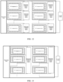
- FIG. 12 illustrates a photovoltaic array using a single-control type photovoltaic component control device.
- the photovoltaic array may be composed of a plurality of photovoltaic components connected in series and parallel. According to a coordinate arrangement, positions and marks of n ⁇ m components can be obtained.
- Each photovoltaic component may be connected to the bypass-type rapid control device. When an accident of the photovoltaic component occurs, a bypass module connected in parallel to the photovoltaic component can be rapidly turned on to protect the component from a short circuit and ensure the safety of the power system.
- the single-control type photovoltaic component control device can realize the status monitoring of a single component.
- FIG. 13 illustrates a photovoltaic array using a multi-control type photovoltaic component control device.
- the photovoltaic array may obtain power from a single photovoltaic component using a bypass-type rapid turn-off device multi-component and supply the power to the controller 30 and other components.
- the controller 30 can realize the bypass protection mechanism of a plurality of photovoltaic components, thereby reducing cost.
Landscapes
- Engineering & Computer Science (AREA)
- Power Engineering (AREA)
- Protection Of Static Devices (AREA)
- Photovoltaic Devices (AREA)
Applications Claiming Priority (1)
| Application Number | Priority Date | Filing Date | Title |
|---|---|---|---|
| CN202311111808.2A CN119543267A (zh) | 2023-08-31 | 2023-08-31 | 光伏组件控制装置 |
Publications (1)
| Publication Number | Publication Date |
|---|---|
| EP4518078A1 true EP4518078A1 (de) | 2025-03-05 |
Family
ID=90717661
Family Applications (1)
| Application Number | Title | Priority Date | Filing Date |
|---|---|---|---|
| EP24167940.6A Pending EP4518078A1 (de) | 2023-08-31 | 2024-03-30 | Vorrichtung zur steuerung von fotovoltaischen komponenten |
Country Status (4)
| Country | Link |
|---|---|
| US (1) | US12456871B2 (de) |
| EP (1) | EP4518078A1 (de) |
| JP (1) | JP7711277B2 (de) |
| CN (1) | CN119543267A (de) |
Families Citing this family (1)
| Publication number | Priority date | Publication date | Assignee | Title |
|---|---|---|---|---|
| CN120200189B (zh) * | 2025-05-23 | 2025-11-04 | 比亚迪股份有限公司 | 光伏系统、电子电气设备和车辆 |
Citations (2)
| Publication number | Priority date | Publication date | Assignee | Title |
|---|---|---|---|---|
| EP2779250A2 (de) * | 2013-03-15 | 2014-09-17 | Solantro Semiconductor Corp. | Photovoltaische Überbrückungs- und Ausgangsschaltung |
| US20180248359A1 (en) * | 2017-02-28 | 2018-08-30 | Sungrow Power Supply Co., Ltd. | Photovoltaic rapid shutdown device and photovoltaic system |
Family Cites Families (8)
| Publication number | Priority date | Publication date | Assignee | Title |
|---|---|---|---|---|
| JP5626798B2 (ja) | 2011-02-04 | 2014-11-19 | シャープ株式会社 | 太陽光発電システム、スイッチングシステム、およびバイパス装置 |
| GB2498365A (en) * | 2012-01-11 | 2013-07-17 | Solaredge Technologies Ltd | Photovoltaic module |
| TW201349731A (zh) | 2012-05-30 | 2013-12-01 | 台達電子工業股份有限公司 | 具有發電模組之太陽能發電系統及其輸出電能控制方法 |
| US20130328404A1 (en) | 2012-06-11 | 2013-12-12 | Panasonic Corporation | Voltage conversion apparatus, power generation system, and voltage conversion method |
| JP6332244B2 (ja) | 2015-11-25 | 2018-05-30 | 三菱電機株式会社 | 太陽光発電システム、太陽電池モジュール間電路開閉器および太陽電池モジュール |
| CN109067353B (zh) * | 2018-08-24 | 2020-03-24 | 阳光电源股份有限公司 | 一种光伏组件的有源旁路控制装置与方法 |
| US11545931B2 (en) | 2019-11-10 | 2023-01-03 | Maxout Renewables, Inc. | Optimizing hybrid inverter system |
| US12218509B2 (en) * | 2022-07-05 | 2025-02-04 | OPTiVOLTS, LLC | Methods and apparatus for optimizing efficiencies of a solar power system |
-
2023
- 2023-08-31 CN CN202311111808.2A patent/CN119543267A/zh active Pending
-
2024
- 2024-03-30 EP EP24167940.6A patent/EP4518078A1/de active Pending
- 2024-05-01 US US18/651,803 patent/US12456871B2/en active Active
- 2024-07-11 JP JP2024111433A patent/JP7711277B2/ja active Active
Patent Citations (2)
| Publication number | Priority date | Publication date | Assignee | Title |
|---|---|---|---|---|
| EP2779250A2 (de) * | 2013-03-15 | 2014-09-17 | Solantro Semiconductor Corp. | Photovoltaische Überbrückungs- und Ausgangsschaltung |
| US20180248359A1 (en) * | 2017-02-28 | 2018-08-30 | Sungrow Power Supply Co., Ltd. | Photovoltaic rapid shutdown device and photovoltaic system |
Also Published As
| Publication number | Publication date |
|---|---|
| US12456871B2 (en) | 2025-10-28 |
| JP7711277B2 (ja) | 2025-07-22 |
| US20250079849A1 (en) | 2025-03-06 |
| JP2025036129A (ja) | 2025-03-14 |
| CN119543267A (zh) | 2025-02-28 |
Similar Documents
| Publication | Publication Date | Title |
|---|---|---|
| US11979037B2 (en) | Photovoltaic module | |
| US7843085B2 (en) | Systems for highly efficient solar power | |
| US20110285375A1 (en) | Maximum Power Point Tracker Bypass | |
| US20090079385A1 (en) | Solar powered battery charger using switch capacitor voltage converters | |
| EP3297117B1 (de) | Verteiltes leistungserzeugungssystem mit einer solarzellenanordnung, einem gleichspannungswandler und einem wechselrichterr | |
| CN104052391B (zh) | 光伏旁路和输出开关装置和方法 | |
| WO2021003728A1 (zh) | 一种应用于光伏发电系统的变换器、方法及系统 | |
| US12456871B2 (en) | Photovoltaic component control device | |
| CN217406513U (zh) | 一种包含单线盒嵌入式接线盒的光伏组件快速关断装置 | |
| CN116915169B (zh) | 光伏电池旁路电路 | |
| AU2019321446B2 (en) | Two-terminal protective device using parasitic energy harvesting | |
| KR20230006275A (ko) | 멀티레벨 구조를 가지는 전력변환장치 | |
| US12107538B2 (en) | Photovoltaic system and power supply system | |
| US12633751B2 (en) | Power-taking circuit, parallel-type photovoltaic component control device, and photovoltaic string power distribution system | |
| US20250286382A1 (en) | Power-taking circuit, parallel-type photovoltaic component control device, and photovoltaic string power distribution system | |
| CN218301235U (zh) | 一种关断器及其自驱动电路 | |
| CN120357751B (zh) | 一种mppt宽范围输入及多电压输出辅助源电路 | |
| CN207251284U (zh) | 供电装置和照明系统 | |
| CN110854985A (zh) | 一种基于dsp的最大功率独立供电系统 | |
| CN219718171U (zh) | 一种太阳能电池设备 | |
| CN222423215U (zh) | 逆变器的控制保护电路和逆变系统 | |
| CN215010108U (zh) | 太阳能电池充放电控制电路 | |
| CN114584066B (zh) | 一种光伏组件关断电路及光伏设备 | |
| US20240079615A1 (en) | Rapid shutdown system of energy storage device | |
| CN205545130U (zh) | 应用于太阳能电池板的低压降旁路保护装置 |
Legal Events
| Date | Code | Title | Description |
|---|---|---|---|
| PUAI | Public reference made under article 153(3) epc to a published international application that has entered the european phase |
Free format text: ORIGINAL CODE: 0009012 |
|
| STAA | Information on the status of an ep patent application or granted ep patent |
Free format text: STATUS: REQUEST FOR EXAMINATION WAS MADE |
|
| 17P | Request for examination filed |
Effective date: 20240330 |
|
| AK | Designated contracting states |
Kind code of ref document: A1 Designated state(s): AL AT BE BG CH CY CZ DE DK EE ES FI FR GB GR HR HU IE IS IT LI LT LU LV MC ME MK MT NL NO PL PT RO RS SE SI SK SM TR |