EP4518155A1 - Suppression d'interférence en mode commun dans un circuit amplificateur pour un dispositif de neuromodulation - Google Patents
Suppression d'interférence en mode commun dans un circuit amplificateur pour un dispositif de neuromodulation Download PDFInfo
- Publication number
- EP4518155A1 EP4518155A1 EP23193810.1A EP23193810A EP4518155A1 EP 4518155 A1 EP4518155 A1 EP 4518155A1 EP 23193810 A EP23193810 A EP 23193810A EP 4518155 A1 EP4518155 A1 EP 4518155A1
- Authority
- EP
- European Patent Office
- Prior art keywords
- voltage signal
- amplifier
- amplifier circuit
- transconductor
- inverting input
- Prior art date
- Legal status (The legal status is an assumption and is not a legal conclusion. Google has not performed a legal analysis and makes no representation as to the accuracy of the status listed.)
- Pending
Links
Images




Classifications
-
- A—HUMAN NECESSITIES
- A61—MEDICAL OR VETERINARY SCIENCE; HYGIENE
- A61N—ELECTROTHERAPY; MAGNETOTHERAPY; RADIATION THERAPY; ULTRASOUND THERAPY
- A61N1/00—Electrotherapy; Circuits therefor
- A61N1/02—Details
- A61N1/025—Digital circuitry features of electrotherapy devices, e.g. memory, clocks, processors
-
- H—ELECTRICITY
- H03—ELECTRONIC CIRCUITRY
- H03F—AMPLIFIERS
- H03F3/00—Amplifiers with only discharge tubes or only semiconductor devices as amplifying elements
- H03F3/45—Differential amplifiers
- H03F3/45071—Differential amplifiers with semiconductor devices only
- H03F3/45076—Differential amplifiers with semiconductor devices only characterised by the way of implementation of the active amplifying circuit in the differential amplifier
- H03F3/45179—Differential amplifiers with semiconductor devices only characterised by the way of implementation of the active amplifying circuit in the differential amplifier using MOSFET transistors as the active amplifying circuit
- H03F3/45237—Complementary long tailed pairs having parallel inputs and being supplied in series
- H03F3/45246—Folded cascode stages
-
- A—HUMAN NECESSITIES
- A61—MEDICAL OR VETERINARY SCIENCE; HYGIENE
- A61B—DIAGNOSIS; SURGERY; IDENTIFICATION
- A61B5/00—Measuring for diagnostic purposes; Identification of persons
- A61B5/24—Detecting, measuring or recording bioelectric or biomagnetic signals of the body or parts thereof
- A61B5/30—Input circuits therefor
- A61B5/305—Common mode rejection
-
- A—HUMAN NECESSITIES
- A61—MEDICAL OR VETERINARY SCIENCE; HYGIENE
- A61N—ELECTROTHERAPY; MAGNETOTHERAPY; RADIATION THERAPY; ULTRASOUND THERAPY
- A61N1/00—Electrotherapy; Circuits therefor
- A61N1/18—Applying electric currents by contact electrodes
- A61N1/32—Applying electric currents by contact electrodes alternating or intermittent currents
- A61N1/36—Applying electric currents by contact electrodes alternating or intermittent currents for stimulation
- A61N1/36014—External stimulators, e.g. with patch electrodes
- A61N1/36017—External stimulators, e.g. with patch electrodes with leads or electrodes penetrating the skin
-
- A—HUMAN NECESSITIES
- A61—MEDICAL OR VETERINARY SCIENCE; HYGIENE
- A61N—ELECTROTHERAPY; MAGNETOTHERAPY; RADIATION THERAPY; ULTRASOUND THERAPY
- A61N1/00—Electrotherapy; Circuits therefor
- A61N1/18—Applying electric currents by contact electrodes
- A61N1/32—Applying electric currents by contact electrodes alternating or intermittent currents
- A61N1/36—Applying electric currents by contact electrodes alternating or intermittent currents for stimulation
- A61N1/36014—External stimulators, e.g. with patch electrodes
- A61N1/36025—External stimulators, e.g. with patch electrodes for treating a mental or cerebral condition
-
- A—HUMAN NECESSITIES
- A61—MEDICAL OR VETERINARY SCIENCE; HYGIENE
- A61N—ELECTROTHERAPY; MAGNETOTHERAPY; RADIATION THERAPY; ULTRASOUND THERAPY
- A61N1/00—Electrotherapy; Circuits therefor
- A61N1/18—Applying electric currents by contact electrodes
- A61N1/32—Applying electric currents by contact electrodes alternating or intermittent currents
- A61N1/36—Applying electric currents by contact electrodes alternating or intermittent currents for stimulation
- A61N1/36014—External stimulators, e.g. with patch electrodes
- A61N1/3603—Control systems
- A61N1/36031—Control systems using physiological parameters for adjustment
-
- H—ELECTRICITY
- H03—ELECTRONIC CIRCUITRY
- H03F—AMPLIFIERS
- H03F3/00—Amplifiers with only discharge tubes or only semiconductor devices as amplifying elements
- H03F3/45—Differential amplifiers
- H03F3/45071—Differential amplifiers with semiconductor devices only
- H03F3/45076—Differential amplifiers with semiconductor devices only characterised by the way of implementation of the active amplifying circuit in the differential amplifier
- H03F3/45475—Differential amplifiers with semiconductor devices only characterised by the way of implementation of the active amplifying circuit in the differential amplifier using IC blocks as the active amplifying circuit
-
- H—ELECTRICITY
- H03—ELECTRONIC CIRCUITRY
- H03F—AMPLIFIERS
- H03F3/00—Amplifiers with only discharge tubes or only semiconductor devices as amplifying elements
- H03F3/45—Differential amplifiers
- H03F3/45071—Differential amplifiers with semiconductor devices only
- H03F3/45479—Differential amplifiers with semiconductor devices only characterised by the way of common mode signal rejection
- H03F3/45632—Differential amplifiers with semiconductor devices only characterised by the way of common mode signal rejection in differential amplifiers with FET transistors as the active amplifying circuit
- H03F3/45636—Differential amplifiers with semiconductor devices only characterised by the way of common mode signal rejection in differential amplifiers with FET transistors as the active amplifying circuit by using feedback means
- H03F3/45663—Measuring at the active amplifying circuit of the differential amplifier
- H03F3/45668—Controlling the input circuit of the differential amplifier
-
- H—ELECTRICITY
- H03—ELECTRONIC CIRCUITRY
- H03F—AMPLIFIERS
- H03F3/00—Amplifiers with only discharge tubes or only semiconductor devices as amplifying elements
- H03F3/45—Differential amplifiers
- H03F3/45071—Differential amplifiers with semiconductor devices only
- H03F3/45479—Differential amplifiers with semiconductor devices only characterised by the way of common mode signal rejection
- H03F3/45632—Differential amplifiers with semiconductor devices only characterised by the way of common mode signal rejection in differential amplifiers with FET transistors as the active amplifying circuit
- H03F3/45636—Differential amplifiers with semiconductor devices only characterised by the way of common mode signal rejection in differential amplifiers with FET transistors as the active amplifying circuit by using feedback means
- H03F3/45663—Measuring at the active amplifying circuit of the differential amplifier
- H03F3/45677—Controlling the active amplifying circuit of the differential amplifier
-
- H—ELECTRICITY
- H03—ELECTRONIC CIRCUITRY
- H03F—AMPLIFIERS
- H03F2200/00—Indexing scheme relating to amplifiers
- H03F2200/129—Indexing scheme relating to amplifiers there being a feedback over the complete amplifier
-
- H—ELECTRICITY
- H03—ELECTRONIC CIRCUITRY
- H03F—AMPLIFIERS
- H03F2200/00—Indexing scheme relating to amplifiers
- H03F2200/261—Amplifier which being suitable for instrumentation applications
-
- H—ELECTRICITY
- H03—ELECTRONIC CIRCUITRY
- H03F—AMPLIFIERS
- H03F2203/00—Indexing scheme relating to amplifiers with only discharge tubes or only semiconductor devices as amplifying elements covered by H03F3/00
- H03F2203/45—Indexing scheme relating to differential amplifiers
- H03F2203/45406—Indexing scheme relating to differential amplifiers the CMCL comprising a common source node of a long tail FET pair as an addition circuit
-
- H—ELECTRICITY
- H03—ELECTRONIC CIRCUITRY
- H03F—AMPLIFIERS
- H03F2203/00—Indexing scheme relating to amplifiers with only discharge tubes or only semiconductor devices as amplifying elements covered by H03F3/00
- H03F2203/45—Indexing scheme relating to differential amplifiers
- H03F2203/45441—Indexing scheme relating to differential amplifiers the CMCL comprising an integrating circuit
-
- H—ELECTRICITY
- H03—ELECTRONIC CIRCUITRY
- H03F—AMPLIFIERS
- H03F2203/00—Indexing scheme relating to amplifiers with only discharge tubes or only semiconductor devices as amplifying elements covered by H03F3/00
- H03F2203/45—Indexing scheme relating to differential amplifiers
- H03F2203/45512—Indexing scheme relating to differential amplifiers the FBC comprising one or more capacitors, not being switched capacitors, and being coupled between the LC and the IC
-
- H—ELECTRICITY
- H03—ELECTRONIC CIRCUITRY
- H03F—AMPLIFIERS
- H03F2203/00—Indexing scheme relating to amplifiers with only discharge tubes or only semiconductor devices as amplifying elements covered by H03F3/00
- H03F2203/45—Indexing scheme relating to differential amplifiers
- H03F2203/45524—Indexing scheme relating to differential amplifiers the FBC comprising one or more active resistors and being coupled between the LC and the IC
Definitions
- the present disclosure provides a neuromodulation device for measuring a biological electrical signal in response to a neural modulation of biological tissue.
- the neuromodulation device comprises at least one amplifier circuit, which is used to amplify an input voltage signal that is based on the biological electrical signal.
- the amplifier circuit provided by this disclosure is configured to suppress a common mode (CM) voltage signal in the input voltage signal, and consequently to reduce CM interference (CMI).
- CM common mode
- a bi-directional (i.e., closed loop) neural interface may be used by a device to perform both neural stimulation and recording.
- a device enables neuromodulation - i.e., is referred to as a neuromodulation device - which is useful for neuroscience studies and treatments of neurological disorders.
- an amplifier circuit (also referred to as neural amplifier) is required, and should be able to perform low-noise small-signal amplification, while at the same time rejecting a large electrode DC offset (EDO).
- EDO electrode DC offset
- capacitively coupled architectures have been widely adopted for such amplifier circuits, since the input capacitors exhibit infinite impedance at DC, and thus prevent the EDO from being amplified.
- a differential inverter-based transconductor is advantageously used in the amplifier circuit, since it provides a higher transconductance than other well-known types of transconductor (e.g., simple wide-swing, or folded cascode).
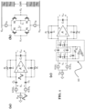
- FIG. 1(a) An example of a conventional capacitively coupled amplifier circuit that may be used in a neuromodulation device is shown in FIG. 1(a) .
- the amplifier circuit has an inverter as input stage, which is shown in FIG. 1(b) .
- the amplifier circuit of FIG. 1(a) When recording in a controlled environment, the amplifier circuit of FIG. 1(a) performs reasonably well, since there is no severe CMI disturbing its performance. However, for a bi-directional neural interface, the amplifier circuit may suffer from CMI due to its limited CM range (CMR).
- CMR CM range
- the stimulation signal can partially propagate to the input (recording and reference electrodes) of the amplifier circuit of FIG. 1(a) , as a stimulation waveform-like CM voltage ( V CM , also referred to as CM voltage signal).
- V CM stimulation waveform-like CM voltage
- the V CM can travel to appear at the input of the amplifier circuit, if the stimulation frequency is higher than f h (and it mostly is).
- the CMR of the amplifier is limited to V DD -V SS -( V B 1 + V B 2 + VGS n + VSG p ), where V B 1 and V B 2 are minimum voltage drops required by tail current sources I B 1 and I B 2 , respectively.
- the other parameters have their own usual meanings.
- the V CM can be in the range of 50-300 mV or even greater. For these reasons, the input stage of FIG. 1(b) cannot always handle the V CM , and consequently the amplification of the amplifier circuit of FIG. 1(a) may fail.
- CMFF CM feedforward
- the CMFF amplifier contains a transconductor (A), a pair of CM detector capacitors C ic , a feedback capacitor C cf , a resistor R cf , and current stealing capacitors C oc .
- This amplifier circuit detects and amplifies the V CM with an AC gain of - 2 C ic / C cf .
- the input CM current flowing through C in i.e., I CM
- the inverter based input stage can remain functioning for V CMpp > CMR.
- the additional CMFF amplifier shown in FIG. 1(c) adds more input capacitor C ic in addition to the original C in , thereby degrading the input impedance of the amplifier circuit.
- IRN input-referred noise
- the amplifier circuit of FIG. 1(c) may further incorporate an impedance boosting network, which leads to additional hardware complexity.
- the chip area per channel needs to be kept tiny, so as to accommodate several hundreds of channels or more within a reasonable total chip area. The large chip area per channel as required by the design of FIG. 1(c) may thus not be acceptable.
- this disclosure aims to provide an improved amplifier circuit for a neuromodulation device, in particular, to overcome the above-mentioned issues.
- An objective is accordingly to suppress a CM voltage signal and reduce CMI, while keeping the size of the amplifier circuit small.
- a further objective is to avoid input impedance degradation.
- An objective is also the performance of the amplifier circuit for low-noise small-signal amplification, and that the amplifier circuit at the same time rejects large EDO.
- Another objective of this disclosure is to provide an improved neuromodulation device.
- a first aspect of this disclosure provides an amplifier circuit for amplifying a biological electrical signal, the amplifier circuit comprising: an input stage with two input terminals, configured to receive an input voltage signal, which is based on the biological electrical signal and comprises a CM voltage signal and a differential mode (DM) voltage signal; a differential transconductor comprising a non-inverting input and an inverting input, each connected to one of the two input terminals, and comprising an output for providing an output current signal based on the DM voltage signal; wherein the transconductor is configured to provide a first CM voltage signal, which is tapped after the non-inverting input, and a second CM voltage signal, which is tapped after the inverting input; and a CM amplifier configured to combine the first CM voltage signal with the second CM voltage signal to obtain a combined CM voltage signal, amplify the combined CM voltage signal with an inverting gain to obtain an inverted CM voltage signal, and provide the inverted CM voltage signal to the non-inverting input and
- the CM amplifier of the amplifier circuit of the first aspect suppresses the CM voltage signal in the input signal and reduces CMI. Since the amplifier circuit comprises the CM amplifier after the transconductor, input impedance degradation is avoided. Also, the size of the amplifier circuit can be smaller than, for example, the amplifier circuit shown in FIG. 1(c) . Due to the differential transconductor, a good low-noise performance of the amplifier circuit can be achieved.
- the amplifier circuit comprises: a first capacitive feedback line configured to feedback the inverted CM voltage signal from the CM amplifier to the non-inverting input of the transconductor; and a second capacitive feedback line configured to feedback the inverted CM voltage signal from the CM amplifier to the inverting input of the transconductor; wherein each of the first and the second capacitive feedback line comprises a first capacitor.
- each of the non-inverting input and the inverting input of the transconductor is connected to one of the two input terminals of the input stage via a respective second capacitor; and the second capacitor has a higher capacitance than the first capacitor.
- the capacitive feedback from the CM amplifier according to the above implementations leads to low noise in the amplifier circuit.
- the transconductor comprises: a first transistor connected with its gate to the non-inverting input and coupled with its source to a supply voltage, VDD; a second transistor connected with its gate to the inverting input, connected with its source to the source of the first transistor, and coupled with its source to VDD; a third transistor connected with its gate to the non-inverting input, connected with its drain to the drain of the first transistor, and coupled with its source to a ground voltage; and a fourth transistor connected with its gate to the inverting input, connected with its drain to the drain of the second transistor, connected with its source to the source of the third transistor, and coupled with its source to VSS; wherein the first CM voltage signal is tapped between the sources of the first and the second transistor, and the second CM voltage signal is tapped between the sources of the third and the fourth transistor.
- the amplifier circuit is configured such that a tail current of the source-connected third and fourth transistor is higher than a tail current of the source-connected first and second transistor in use of the amplifier circuit.
- the CM amplifier comprises a summing junction at which the first CM voltage signal and the second CM voltage signal are combined into the combined CM voltage signal; wherein each of the first CM voltage signal and the second CM voltage signal is connected to the combination point via a respective third capacitor.
- the CM amplifier further comprises a gain circuit including a second transconductor, a fourth capacitor and a first resistor; and the gain circuit is configured to amplify the combined CM voltage signal with the inverting gain to produce the inverted CM voltage signal.
- the amplifier circuit further comprises a DM feedback circuit configured to provide a feedback voltage signal, which is based on the output current signal of the transconductor, to the non-inverting input and the inverting input of the transconductor.
- the capacitively coupled feedback architecture of the above implementations achieves the desired EDO rejecting abilities of the amplifier circuit.
- the amplifier circuit further comprises a conversion circuit configured to convert the output current signal of the transconductor into the feedback voltage signal.
- the biological electrical signal is an electroencephalogram, (EEG) signal or a stimulation-based neural signal.
- EEG electroencephalogram
- a second aspect of this disclosure provides a neuromodulation device for measuring one or more biological electrical signals in response to a neural modulation of biological tissue, wherein the neuromodulation device comprises one or more amplifier circuits of the first aspect or any implementation thereof.
- the neuromodulation device further comprises an array of electrodes comprising a first set of electrodes and a second set of electrodes, wherein each electrode of the first set is connected to a respective amplifier circuit of the one or more amplifier circuits, and wherein each electrode of the second set is configured to cause a respective neural modulation of the biological tissue.
- some electrodes can be used for recording, and some other electrodes for stimulating, which may be beneficial for the performance of the neuromodulation device.
- each electrode of the second set comprises a stimulator, which is configured to provide a stimulation signal to cause the neural modulation of the biological tissue.
- the neuromodulation device comprises multiple of the amplifier circuits; wherein the amplifier circuits share a single CM amplifier; and the CM amplifier is configured to provide, for each of the amplifier circuits, a respective inverted CM voltage signal to the non-inverting input and the inverting input of the transconductor of that amplifier circuit.
- the neuromodulation device further comprises one or more shared buffers connected to the multiple amplifier circuits and to the single CM amplifier, wherein the output of each amplifier circuit is connected by a respective switch to the shared buffers; wherein the neuromodulation device is configured to sequentially operate the switches, which causes the multiple amplifier circuits to sequentially output their respective current signal and causes the CM amplifier to sequentially provide the respective inverted CM voltage signal to the respective transconductor of one of the amplifier circuits.
- the shared buffers allow multiplexing the multiple channels.
- the neuromodulation device further comprises a bi-directional neural interface comprising at least one needle; wherein the neural interface is configured to provide the neural stimulation to the biological tissue, to receive the one or more biological electrical signals, and to provide them to the one or more amplifier circuits.
- the neuromodulation device of the second aspect achieves the same advantages as the amplifier circuit of the first aspect.
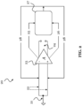
- FIG. 2 shows an amplifier circuit 20 according to this disclosure.
- the amplifier circuit 20 is configured to amplify a biological electrical signal, for instance, as received in response to a neural modulation of biological tissue. That is, the biological electrical signal maybe a stimulation-based neural signal.
- the biological electrical signal may, for example, be an EEG signal.
- the amplifier circuit 20 is suitable for use in a neuromodulation device or a recording arrangement. Due to its low-noise performance and efficient CM suppression, the amplifier circuit 20 is especially suited for a neuromodulation device using a bi-directional neural interface for neural stimulation and signal recording.
- the amplifier circuit 20 shown in FIG. 2 comprises an input stage 21 with two input terminals, a differential transconductor 23, and a CM amplifier 27.
- the input stage 21 is configured to receive an input voltage signal 22, which is based on the biological electrical signal that the amplifier circuit 20 is intended to amplify.
- the input voltage signal 22 may be derived from the biological electrical signal, or may be the biological electrical signal, or the biological electrical signal may be signal processed to obtain the input voltage signal 22.
- the input voltage signal 22 comprises a CM voltage signal and a DM voltage signal.
- the DM voltage signal is the signal component, which the amplifier circuit 20 is supposed to amplify, while the CM voltage signal is the signal component that the amplifier circuit 20 is designed to suppress.
- the CM amplifier 27 is configured to combine the first CM voltage signal 25 with the second CM voltage signal 26, so as to obtain a combined CM voltage signal. For instance, the first and second CM voltage signal 25, 26 may be summed. Then, the CM amplifier 27 is configured to amplify the combined CM voltage signal with an inverting gain, so as to obtain an inverted CM voltage signal 28. This inverted CM voltage signal 28 is then provided back to the non-inverting input and the inverting input of the transconductor 23, respectively, as indicated in FIG. 2 . This feedback leads to a suppression of the CM voltage signal in the output current signal of the transconductor 23.
- FIG. 3 shows an exemplary and more detailed amplifier circuit 20 according to this disclosure, which builds on the amplifier circuit 20 shown in FIG. 2 . Same components in FIG. 2 and FIG. 3 share the same reference signs and function likewise.
- the amplifier circuit 20 shown in FIG. 3 comprises capacitive feedback lines to provide the inverted CM voltage signal 28 back to the inputs of the transconductor 23.
- the feedback lines of the amplifier circuit include a first capacitive feedback line 31, which is configured to feedback the inverted CM voltage signal 28 from the CM amplifier 27 to the non-inverting input of the transconductor 23, and a second capacitive feedback line 32, which is configured to feedback the inverted CM voltage signal 28 from the CM amplifier 27 to the inverting input of the transconductor 23.
- Both capacitive feedback lines 31 and 32 comprise a capacitor C co .
- the amplifier circuit 20 comprises further capacitors.
- the amplifier circuit 20 comprises a capacitor C L at the output 24, in particular, between two output terminals of the output 24.
- the amplifier circuit 20 comprises two capacitors C in .
- both the non-inverting input and the inverting input of the transconductor 23 may be connected via one capacitor C in to the input stage 21.
- the capacitors C in are preferably selected such that they have (each) a higher capacitance than the capacitors C co .
- the amplifier circuit 20 further comprises a DM feedback circuit 33, which is configured to provide a feedback voltage signal 34, which is based on the output current signal of the transconductor 23 - which is again based on the DM voltage signal in the input voltage signal 22 - to the two inputs of the transconductor 23.
- the DM feedback circuit 33 comprises a first and a second capacitive feedback path, wherein each feedback path comprises a capacitor C f and a resistor R f that is connected in parallel to C f .
- FIG. 4 shows an exemplary transistor-level implementation of an amplifier circuit 20 according to this disclosure, for example, the amplifier circuit 20 shown in FIG. 3 .
- Same components in FIG. 3 and FIG. 4 share the same reference signs and function likewise.
- the transconductor 23 comprises four transistors M 1 , M 2 , M 3 , and M 4 .
- the first transistor M 1 is connected with its source to the source of the second transistor M 2 .
- the third transistor M 3 is connected with its source to the source of the fourth transistor M 4 .
- the pair M 1 -M 2 and the pair M 3 -M 4 is, respectively, a source-connected transistor pair. These two transistor pairs are connected to each other.
- the first transistor M 1 is connected with its drain to the drain of the third transistor M 3
- the second transistor M 2 is connected with its drain to the drain of the fourth transistor M 4 .
- the gates of the first transistor M 1 and the third transistor M 3 are both connected to the non-inverting input, and the gates of the second transistor M 2 and the fourth transistor M 4 are both connected to the inverting input.
- the connected sources of the first transistor M 1 and the second transistor M 2 are further coupled to V DD , e.g., via a current source, and the connected sources of the third transistor M 3 and the fourth transistor M 4 are further coupled to Vss, e.g., via a current source.
- V DD voltage source
- Vss e.g., via a current source
- the first CM voltage signal 25 is tapped between the sources of the first and the second transistor M 1 , M 2
- the second CM voltage signal 26 is tapped between the sources of the third and the fourth transistor M 3 , M 4 , for instance, at the respective coupling connection of these sources to either V DD and Vss.
- CM voltage signals 25, 26 are provided to the CM amplifier 27, in particular, are routed to a summing junction 42.
- the lines carrying the first CM voltage signal 25 and the second CM voltage signal 26 may be respectively connected to the summing junction 42 via a respective capacitor C ci .
- the first CM voltage signal 25 and the second CM voltage signal 26 are combined, i.e., added together. This results in the combined CM voltage signal.
- the combined CM voltage signal is further provided to a gain circuit 43 of the CM amplifier 27.
- the gain circuit 43 includes a transconductor Ac, a capacitor C cf and a resistor R cf as shown, and is configured to amplify the combined CM voltage signal with the inverting gain (negative gain), which results in the inverted CM voltage signal 28.
- the inverted voltage signal 28 is provided via the capacitive feedback lines 31, 32 to the inverting and non-inverting input of the transconductor 23.
- An underlying concept of the amplifier circuits 20 shown in the FIGs. 2-4 is that instead of detecting the CM voltage signal at the input stage 21 and performing feedforward cancellation - as shown for the exemplary amplifier circuit of FIG. 1(c) - the CM voltage signal of the input voltage signal 22 is allowed to enter the transconductor 23, and a feedback-based CM suppression is performed. This helps to avoid the undesired input impedance degradation.
- V iCM 1 V iCM 2 ⁇ 2 V cmH ⁇ 2 V cmL .
- the inverted CM voltage signal 28 is fed back to the input terminals of the transconductor 23, via the feedback lines 31, 32 including the capacitors C co .
- V iCM V CM 2 C in 2 C in + C EQ ⁇ V CM C in C in + KC OC
- V iCM becomes zero, meaning that there are no CM voltage fluctuations at the inputs of the transconductor 23.
- C CO « C in for noise reasons.
- K a practical value of K >50 is desirable.
- V CO maybe seen as AC ground, and the pair of capacitors C CO (without gain) may be virtually grounded.
- This is to allow folded-cascode branches (M 5 -I B2 and M 6 -I B2 ) to deliver the output current of the input stage to the output nodes V o1 and V o2 , respectively.
- This topology offers a wide signal swing at the output.
- the output common mode feedback block (CMFB) may be is inserted to create a CM feedback loop to stabilize the output CM level of V o1 and V o2 .
- V B is to bias the common gate voltage of M 5 and M 6 .
- the source-coupled transistor pairs M 1 -M 2 and M 3 -M 4 are also able to detect CM voltage fluctuations, and shift them to appear at the common source terminals of the two transistor pairs as V cmH and V cmL , respectively.
- the CM amplifier 27, which may be formed by formed by C ci , C cf , R cf and the transconductor Ac, will perform CM signal amplification with a gain of -K -2 C ci / C cf .
- the resistor R cf can be made by a MOS pseudo-resistor.
- a high-pass cut-off frequency below 1 Hz can be achieved within a tiny chip area.
- the transconductor A C only contributes CM noise that can be cancelled out in the differential mode. It can thus be designed in a compact and low-power fashion. Therefore, a large K can be achieved within a reasonable area.
- FIG. 5 compares exemplary output voltages of an amplifier circuit without CMI suppression (shown in FIG. 1(a) ) and an amplifier circuit 20 comprising the CM amplifier 27 according to this disclosure.
- the comparison shows that a large CMI will exceed the CMR of the exemplary amplifier circuit, which may shutdown the amplifier circuit as visible in FIG. 5(a) .
- the amplifier circuit 20 of this disclosure is more robust, as the CM is suppressed, and brings back a clean output signal in FIG. 5(b) .
- FIG. 5(a) shows the output voltage of the exemplary amplifier circuit without the CM amplifier 27 and without capacitive feedback via C CO over time.
- the amplifier circuit fails to provide any output signal. This implies, for instance, that reading a neural signal at a stimulation moment would not be possible.
- the proper sinusoidal output voltage signal can be obtained, as shown in FIG. 5(b) . Recording a neural signal during stimulation is possible in this case, i.e., with the amplifier circuit 20 of this disclosure.
- V CM sinusoidal sinusoidal V CM with a 200 mV p amplitude
- the resistors R f and R cf were identically made by MOS pseudo-resistors.
- OTA operational transconductance amplifier
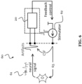
- FIG. 6 shows an exemplary neuromodulation device 60 according to this disclosure.
- the neuromodulation device 60 is configured to measure one or more biological electrical signals 61 in response to a neural modulation of biological tissue.
- the neuromodulation device 60 comprises at least one amplifier circuits 20 according to this disclosure, for instance, as described in the FIGs. 2-4 .
- the neuromodulation device 60 may further comprises at least one stimulator 62, which is configured to generate a stimulation signal 63, which can cause the neural modulation of the biological tissue.
- the stimulation signal 63 may be provided by a neural interface of the neuromodulation device 60 to the biological tissue.
- the neural interface may be a bi-directional neural interface, which is further configured to receive the one or more biological electrical signals 61 in response to the neural stimulation, and to provide them to the one or more amplifier circuits 20.
- the neuromodulation device 60 may comprise a bi-directional neural interface comprising at least one needle 74.
- the neuromodulation device 60 may comprise an array 71 of electrodes.
- the array 71 may include a first set of electrodes 72 and a second set of electrodes 73, which may be of a different kind or design.
- each electrode 72 of the first set may be connected to a respective amplifier circuit 20 of the one or more amplifier circuits 20 of the neuromodulation device 60.
- Each electrode 73 of the second set may be configured to cause a respective neural modulation of the biological tissue.
- each electrode 72 of the first set may comprise at least one amplifier circuit 20, and may be used for measuring (recording) an electrical biological signal 61.
- Each electrode 73 of the second set may comprises at least one stimulator 62, and may be used to generate a stimulation signal 63 to the interface, in this case comprising the needle 74.
- FIG. 8 shows a multichannel recording arrangement 80 according to this disclosure.
- the recording arrangement 80 comprises multiple of the amplifier circuits 20 according to this disclosure, for example, as shown in FIGs. 2-4 .
- Each amplifier circuit 20 maybe associated with one of multiple channels.
- the amplifier circuits 20 share a single CM amplifier 27.
- the CM amplifier 27 may be considered being a part of each amplifier circuit 20.
- the CM amplifier 27 is configured to provide, for each of the amplifier circuits 20, a respective inverted CM voltage signal 28 to the non-inverting input and the inverting input of the transconductor 23 of that amplifier circuit 20.
- the shared CM amplifier 27 may improve the area per channel in the multichannel topology, since it can be shared among many recoding channels. This sharing is possible under the assumption that all recording electrodes (first set of electrodes 72) are placed in the nearby neighborhood and individually suffer from a comparable amount of CMI.
- CM feedback gain i.e., the same degree of CM suppression
- N pairs of C ci / N the same area occupied by one pair of C ci
- a pair of buffers can be used here.
- a pair of C co is still used for each channel.
- This topology also offers weighted adjustment for each channel individually by adjusting the C co value. This is useful, if the strength of the CMI appearing on each channel is known beforehand.
- the CM amplifier 27 may perform summing average of CMI and the required C EQ for each channel, and can be adjusted via the value of C co according to (1) and the known CMI.
- the multichannel recording arrangement 80 of FIG. 8 may further comprises one or more shared buffers 81 (which may be used as ADC drivers), which are connected to the multiple amplifier circuits 20 and to the single CM amplifier 27.
- the output of each amplifier circuit 20 is connected by a respective switch S 1 , S 2 , S 3 ...S N to the shared buffers 81.
- the outputs of all channels (1 to N) may be multiplexed by switches S 1 to S N , and may be controlled by the clock signals shown in timing diagram at the bottom of FIG. 8 . That is, the recording arrangement 80 is configured to sequentially operate the switches S 1 ... S N , which causes the multiple amplifier circuits 20 to sequentially output their respective current signal, and causes the CM amplifier 27 to sequentially provide the respective inverted CM voltage signal 28 to the respective transconductor 23 of one of the amplifier circuits 20.
- An embodiment of this disclosure is further a multichannel neuromodulation device, which comprises the multichannel recording arrangement 80 shown in FIG. 8 .
- this multichannel neuromodulation device may accordingly comprise at least one least one stimulator, which is configured to generate a stimulation signal.
- the multichannel neuromodulation device may be similar to the neuromodulation device 60 of FIG. 6 having multiple channels for recording.
- the neuromodulation device 60 shown in FIG. 6 may comprise the recording arrangement 80 shown in FIG. 8 .
- a stimulation-like waveform of V CM together with sinusoidal V id (as described above with respect to FIG. 5 )) was applied to all channel inputs. Similar results as shown in FIG. 5 were obtained, which proves that the shared CM amplifier 27 is well functional.
- FIG. 9 shows a Discrete Fourier Transform (DFT) of a first channel with and without reset mechanism. A 1 kHz 3 mV p input voltage signal was applied to the first channel. The rest of the channel inputs received the same signal amplitude, but different frequencies that are not set to be clearly visible in frequency domain (not located at any harmonics of the first channel's input signal).
- DFT Discrete Fourier Transform
- FIG. 9(a) shows, for the case that S R are always turned off ( C p are not discharged), that the first channel's output comprises fundamental component at 1 kHz, its 3 rd harmonic component, and the output of the previous recorded channel, i.e., channel 16 (as a crosstalk component with -56 dB magnitude at 3.3 kHz).
- This crosstalk component was stored on C p and added to the output signal of the first channel 1 after S 1 is closed.
- This crosstalk can be minimized by the controlling of the reset switches S R according to the timing diagram in FIG. 8 .
- the result is obtained in FIG. 9(b) .
- the memory of channel 16 stored on C p is erased almost completely.
- the crosstalk component is thus reduced from -56 dB to -92 dB.
- an amplifier circuit 20 configured to suppress a CM voltage signal in the input voltage signal 22, and consequently to reduce CMI, while not degrading the input impedance.
Landscapes
- Health & Medical Sciences (AREA)
- Life Sciences & Earth Sciences (AREA)
- Engineering & Computer Science (AREA)
- Biophysics (AREA)
- Veterinary Medicine (AREA)
- Public Health (AREA)
- General Health & Medical Sciences (AREA)
- Animal Behavior & Ethology (AREA)
- Biomedical Technology (AREA)
- Radiology & Medical Imaging (AREA)
- Nuclear Medicine, Radiotherapy & Molecular Imaging (AREA)
- Heart & Thoracic Surgery (AREA)
- Power Engineering (AREA)
- Child & Adolescent Psychology (AREA)
- Physiology (AREA)
- Neurology (AREA)
- Hospice & Palliative Care (AREA)
- Developmental Disabilities (AREA)
- Social Psychology (AREA)
- Psychology (AREA)
- Psychiatry (AREA)
- Physics & Mathematics (AREA)
- Pathology (AREA)
- Medical Informatics (AREA)
- Molecular Biology (AREA)
- Surgery (AREA)
- Amplifiers (AREA)
Priority Applications (2)
| Application Number | Priority Date | Filing Date | Title |
|---|---|---|---|
| EP23193810.1A EP4518155A1 (fr) | 2023-08-29 | 2023-08-29 | Suppression d'interférence en mode commun dans un circuit amplificateur pour un dispositif de neuromodulation |
| US18/818,054 US20250073450A1 (en) | 2023-08-29 | 2024-08-28 | Common Mode Interference Suppression In An Amplifier Circuit For A Neuromodulation Device |
Applications Claiming Priority (1)
| Application Number | Priority Date | Filing Date | Title |
|---|---|---|---|
| EP23193810.1A EP4518155A1 (fr) | 2023-08-29 | 2023-08-29 | Suppression d'interférence en mode commun dans un circuit amplificateur pour un dispositif de neuromodulation |
Publications (1)
| Publication Number | Publication Date |
|---|---|
| EP4518155A1 true EP4518155A1 (fr) | 2025-03-05 |
Family
ID=87863638
Family Applications (1)
| Application Number | Title | Priority Date | Filing Date |
|---|---|---|---|
| EP23193810.1A Pending EP4518155A1 (fr) | 2023-08-29 | 2023-08-29 | Suppression d'interférence en mode commun dans un circuit amplificateur pour un dispositif de neuromodulation |
Country Status (2)
| Country | Link |
|---|---|
| US (1) | US20250073450A1 (fr) |
| EP (1) | EP4518155A1 (fr) |
Citations (1)
| Publication number | Priority date | Publication date | Assignee | Title |
|---|---|---|---|---|
| US5392784A (en) * | 1993-08-20 | 1995-02-28 | Hewlett-Packard Company | Virtual right leg drive and augmented right leg drive circuits for common mode voltage reduction in ECG and EEG measurements |
-
2023
- 2023-08-29 EP EP23193810.1A patent/EP4518155A1/fr active Pending
-
2024
- 2024-08-28 US US18/818,054 patent/US20250073450A1/en active Pending
Patent Citations (1)
| Publication number | Priority date | Publication date | Assignee | Title |
|---|---|---|---|---|
| US5392784A (en) * | 1993-08-20 | 1995-02-28 | Hewlett-Packard Company | Virtual right leg drive and augmented right leg drive circuits for common mode voltage reduction in ECG and EEG measurements |
Non-Patent Citations (3)
| Title |
|---|
| HONG SOONSEONG ET AL: "A Power-Efficient Low-Noise Neural Recording Amplifier IC with High Tolerance to Stimulation Artifacts", 2022 19TH INTERNATIONAL SOC DESIGN CONFERENCE (ISOCC), IEEE, 19 October 2022 (2022-10-19), pages 306 - 307, XP034289646, DOI: 10.1109/ISOCC56007.2022.10031576 * |
| PÉREZ-PRIETO NORBERTO ET AL: "Recording Strategies for High Channel Count, Densely Spaced Microelectrode Arrays", FRONTIERS IN NEUROSCIENCE, vol. 15, 13 July 2021 (2021-07-13), CH, pages 1 - 21, XP093128989, ISSN: 1662-453X, Retrieved from the Internet <URL:https://www.frontiersin.org/journals/neuroscience/articles/10.3389/fnins.2021.681085/full#B3> DOI: 10.3389/fnins.2021.681085 * |
| XU JIAWEI ET AL: "Active Electrodes for Wearable EEG Acquisition: Review and Electronics Design Methodology", IEEE REVIEWS IN BIOMEDICAL ENGINEERING, vol. 10, 29 December 2017 (2017-12-29), pages 187 - 198, XP011675427, ISSN: 1937-3333, [retrieved on 20171229], DOI: 10.1109/RBME.2017.2656388 * |
Also Published As
| Publication number | Publication date |
|---|---|
| US20250073450A1 (en) | 2025-03-06 |
Similar Documents
| Publication | Publication Date | Title |
|---|---|---|
| US11025215B2 (en) | High input impedance, high dynamic range, common-mode-interferer tolerant sensing front-end for neuromodulation systems | |
| US5573550A (en) | Implantable stimulation device having a low noise, low power, precision amplifier for amplifying cardiac signals | |
| JP4095174B2 (ja) | 液晶ディスプレイ装置 | |
| US8531238B2 (en) | Multi-stage fully differential amplifier with controlled common mode voltage | |
| Duisters et al. | A-90-dB THD rail-to-rail input opamp using a new local charge pump in CMOS | |
| US8004350B2 (en) | Impedance transformation with transistor circuits | |
| JPS58111416A (ja) | 利得制御増幅器 | |
| Tran et al. | An ultra-low-power neural signal acquisition analog front-end IC | |
| US7471148B2 (en) | Differential low noise amplifier (LNA) with common mode feedback and gain control | |
| CN117895909B (zh) | 一种具有高输入阻抗的电容斩波仪表放大器 | |
| US5117200A (en) | Compensation for a feedback amplifier with current output stage | |
| US6023194A (en) | Amplifier with reduced input capacitance | |
| Liu et al. | An auto-zeroing chopper-stabilized capacitively coupled instrumentation amplifier with 25-Vpp common-mode interference tolerance | |
| EP4518155A1 (fr) | Suppression d'interférence en mode commun dans un circuit amplificateur pour un dispositif de neuromodulation | |
| US4521741A (en) | Impedance transformer circuit | |
| KR102615524B1 (ko) | 포지티브 피드백 루프와 네거티브 커패시턴스 방식의 입력 임피던스 증폭 회로 | |
| EP0234107A2 (fr) | Circuits à transistors à effet de champ | |
| Kim et al. | An ultra low-power low-noise neural recording analog front-end IC for implantable devices | |
| Chang et al. | Instrumentation amplifier input capacitance cancellation for biopotential and bioimpedance measurements | |
| US6825708B1 (en) | Apparatus and method for an offset-correcting sense amplifier | |
| US9867574B2 (en) | Multi-channel neural signal amplifier system providing high CMRR across an extended frequency range | |
| CN211959169U (zh) | 一种可编程生物电传感放大器 | |
| Wu et al. | Efficient self-adaptive pseudo-resistor with rapid settling and high linearity for neurorecording front-end circuits | |
| Chen et al. | A Low Noise Neural Recording Frontend IC With Power Management for Closed-Loop Brain-Machine Interface Application | |
| Reich et al. | A self-compensated, low-offset voltage buffer for input impedance boosting in chopped neural front-ends |
Legal Events
| Date | Code | Title | Description |
|---|---|---|---|
| PUAI | Public reference made under article 153(3) epc to a published international application that has entered the european phase |
Free format text: ORIGINAL CODE: 0009012 |
|
| STAA | Information on the status of an ep patent application or granted ep patent |
Free format text: STATUS: THE APPLICATION HAS BEEN PUBLISHED |
|
| AK | Designated contracting states |
Kind code of ref document: A1 Designated state(s): AL AT BE BG CH CY CZ DE DK EE ES FI FR GB GR HR HU IE IS IT LI LT LU LV MC ME MK MT NL NO PL PT RO RS SE SI SK SM TR |
|
| STAA | Information on the status of an ep patent application or granted ep patent |
Free format text: STATUS: REQUEST FOR EXAMINATION WAS MADE |
|
| 17P | Request for examination filed |
Effective date: 20250904 |