EP4521555A1 - Antenneneinheit, antennenanordnung und kommunikationsvorrichtung - Google Patents
Antenneneinheit, antennenanordnung und kommunikationsvorrichtung Download PDFInfo
- Publication number
- EP4521555A1 EP4521555A1 EP23867443.6A EP23867443A EP4521555A1 EP 4521555 A1 EP4521555 A1 EP 4521555A1 EP 23867443 A EP23867443 A EP 23867443A EP 4521555 A1 EP4521555 A1 EP 4521555A1
- Authority
- EP
- European Patent Office
- Prior art keywords
- slit
- patch
- sub
- antenna element
- antenna
- Prior art date
- Legal status (The legal status is an assumption and is not a legal conclusion. Google has not performed a legal analysis and makes no representation as to the accuracy of the status listed.)
- Pending
Links
Images





















Classifications
-
- H—ELECTRICITY
- H01—ELECTRIC ELEMENTS
- H01Q—ANTENNAS, i.e. RADIO AERIALS
- H01Q21/00—Antenna arrays or systems
- H01Q21/06—Arrays of individually energised antenna units similarly polarised and spaced apart
- H01Q21/08—Arrays of individually energised antenna units similarly polarised and spaced apart the units being spaced along or adjacent to a rectilinear path
-
- H—ELECTRICITY
- H01—ELECTRIC ELEMENTS
- H01Q—ANTENNAS, i.e. RADIO AERIALS
- H01Q19/00—Combinations of primary active antenna elements and units with secondary devices, e.g. with quasi-optical devices, for giving the antenna a desired directional characteristic
- H01Q19/005—Patch antenna using one or more coplanar parasitic elements
-
- H—ELECTRICITY
- H01—ELECTRIC ELEMENTS
- H01Q—ANTENNAS, i.e. RADIO AERIALS
- H01Q21/00—Antenna arrays or systems
- H01Q21/24—Combinations of antenna units polarised in different directions for transmitting or receiving circularly and elliptically polarised waves or waves linearly polarised in any direction
-
- H—ELECTRICITY
- H01—ELECTRIC ELEMENTS
- H01Q—ANTENNAS, i.e. RADIO AERIALS
- H01Q5/00—Arrangements for simultaneous operation of antennas on two or more different wavebands, e.g. dual-band or multi-band arrangements
- H01Q5/30—Arrangements for providing operation on different wavebands
- H01Q5/307—Individual or coupled radiating elements, each element being fed in an unspecified way
- H01Q5/342—Individual or coupled radiating elements, each element being fed in an unspecified way for different propagation modes
-
- H—ELECTRICITY
- H01—ELECTRIC ELEMENTS
- H01Q—ANTENNAS, i.e. RADIO AERIALS
- H01Q5/00—Arrangements for simultaneous operation of antennas on two or more different wavebands, e.g. dual-band or multi-band arrangements
- H01Q5/30—Arrangements for providing operation on different wavebands
- H01Q5/378—Combination of fed elements with parasitic elements
- H01Q5/385—Two or more parasitic elements
-
- H—ELECTRICITY
- H01—ELECTRIC ELEMENTS
- H01Q—ANTENNAS, i.e. RADIO AERIALS
- H01Q9/00—Electrically-short antennas having dimensions not more than twice the operating wavelength and consisting of conductive active radiating elements
- H01Q9/04—Resonant antennas
- H01Q9/0407—Substantially flat resonant element parallel to ground plane, e.g. patch antenna
- H01Q9/045—Substantially flat resonant element parallel to ground plane, e.g. patch antenna with particular feeding means
- H01Q9/0457—Substantially flat resonant element parallel to ground plane, e.g. patch antenna with particular feeding means electromagnetically coupled to the feed line
-
- H—ELECTRICITY
- H01—ELECTRIC ELEMENTS
- H01Q—ANTENNAS, i.e. RADIO AERIALS
- H01Q9/00—Electrically-short antennas having dimensions not more than twice the operating wavelength and consisting of conductive active radiating elements
- H01Q9/04—Resonant antennas
- H01Q9/0407—Substantially flat resonant element parallel to ground plane, e.g. patch antenna
- H01Q9/0478—Substantially flat resonant element parallel to ground plane, e.g. patch antenna with means for suppressing spurious modes, e.g. cross polarisation
Definitions
- the present invention relates to the field of radio frequency communication technologies, and in particular, to an antenna element, an antenna array, and a communication device.
- a router and customer premises equipment (customer premises equipment, CPE) are used as an example.
- CPE customer premises equipment
- a pattern-reconfigurable feature of a high Wi-Fi frequency band has become an important selling point in a next-generation smart home solution.
- a low-profile antenna solution is usually designed based on a patch (patch) antenna, and implements high-gain omnidirectional coverage in a horizontal plane by using a phase control method.
- a continuous research and development direction in the industry is how to design a dual-polarized antenna element to ensure that a bandwidth, a gain, and coverage of an antenna meet design requirements while implementing a low profile.
- the antenna element is dual-polarized, to implement a low profile and ensure that a bandwidth, a gain, and coverage of an antenna meet design requirements.
- an embodiment of this application provides an antenna element, including a radiation patch and a feeding assembly, where the radiation patch includes a first additional sub-patch, a first sub-patch, a second sub-patch, and a second additional sub-patch that are sequentially arranged in a first direction, the radiation patch includes a first slit and a second slit that penetrate the radiation patch in a second direction, the first slit is formed between the first sub-patch and the second sub-patch, the second slit includes a first sub-slit and a second sub-slit, the first sub-slit is formed between the first sub-patch and the first additional sub-patch, the second sub-slit is formed between the second sub-patch and the second additional sub-patch, a maximum size of the radiation patch in the first direction is a length of the radiation patch, a maximum size of the radiation patch in the second direction is a width of the radiation patch, and a length-to-width ratio R of the radiation
- This application has an advantage of a low profile by using the radiation patch as a radiator of the antenna element.
- a radiation patch whose length is greater than a width can be used, to reduce a size of the radiation patch in a width direction.
- a size of the radiation patch in the first direction may be limited to be greater than a size of the radiation patch in the second direction, so that the antenna element can generate a fan-shaped beam, to meet a coverage requirement.
- the length-to-width ratio of the radiation patch is limited, so that the antenna element can be limited within a proper bandwidth range.
- the first slit and the second slit that penetrate the radiation patch in the second direction are provided, so that in a process in which the feeding assembly excites the radiation patch, the antenna element can be excited to generate at least two operating modes.
- This application helps implement the low profile of the antenna and ensure a bandwidth and a gain of the antenna.
- the first slit and the second slit each include a first end and a second end, both an extension direction of the first slit and an extension direction of the second slit are a direction in which the first end points to the second end, and both the extension direction of the first slit and the extension direction of the second slit are the second direction.
- specific definitions of the extension direction of the first slit and the extension direction of the second slit are limited, and a specific implementation in which the extension direction is the width direction (the second direction) of the radiation patch is specified.
- specific shapes of the first slit and the second slit may not be limited to rectangles.
- both a length of the first slit and a length of the second slit are a size of an extension path extending from the first end to the second end
- both a width of the first slit and a width of the second slit are a size in a direction perpendicular to the extension path
- both the width of the first slit and the width of the second slit are within a range of 0.03 mm to 3 mm.
- the width of the first slit and the width of the second slit are limited within the range of 0.03 mm to 3 mm, so that the antenna element can be limited within the proper bandwidth range.
- High coverage rate effect is implemented while a high-gain fan-shaped beam is formed. This solution helps ensure that the antenna element can generate two different operating modes in both vertical polarization and horizontal polarization.
- the width of the second slit is less than or equal to 2 mm. In this solution, the width of the second slit is limited, so that the antenna element can be limited within the proper bandwidth range.
- the width of the first slit is 1.2 mm, and the width of the second slit is 0.8 mm.
- the length-to-width ratio R of the radiation patch satisfies 3 ⁇ R ⁇ 5.
- the length-to-width ratio of the radiation patch is limited, so that the antenna element can be limited within a proper bandwidth range.
- the radiation patch does not have a slit that penetrates the radiation patch in the first direction, or the radiation patch has only one slit that penetrates the radiation patch in the first direction.
- the first slit and the second slit that penetrate the radiation patch in the second direction are provided, and the radiation patch does not have a slit that penetrates the radiation patch in the first direction, or has only one slit that penetrates the radiation patch in the first direction, so that in a process in which a first feed structure and a second feed structure excite the radiation patch, the antenna element can be excited to generate two different polarizations, and each polarization has two operating modes.
- This application helps implement the low profile of the antenna and ensure the bandwidth and the gain of the antenna.
- the first slit is in a middle position of the radiation patch in the first direction. Because the second slit penetrates the radiation patch in the second direction and the second slit is symmetrically distributed on two sides of the first slit in the first direction, in this solution, the middle position is limited only to the middle position of the radiation patch in the first direction, and whether the middle position is a middle position in the second direction is not limited. In this solution, the first slit is limited to be symmetrically distributed on the two sides of the first slit, so that the radiation patch forms a symmetrical distribution architecture centered on the first slit. This helps control a beam pattern of the antenna element.
- a plurality of sub-patches are symmetrically distributed on the two sides of the first slit in the first direction.
- the plurality of sub-patches of the radiation patch are limited to forming the symmetrical distribution architecture centered on the first slit. This helps control the beam pattern of the antenna element.
- the feeding assembly includes a ground plane and a feeding layer, the ground plane is disposed between the feeding layer and the radiation patch in a stacked manner, the feeding layer includes a first feed structure and a second feed structure, the ground plane is provided with a first coupling slit and a second coupling slit that are provided in a cross manner, the first feed structure and the first coupling slit are provided directly opposite to each other, and the second feed structure and the second coupling slit are provided directly opposite to each other.
- the first coupling slit at least partially overlaps the first sub-patch
- the first coupling slit at least partially overlaps the second sub-patch
- the second coupling slit is provided directly opposite to the first slit.
- the first feed structure is coupled to the first coupling slit to excite first polarization of the radiation patch.
- the second coupling slit does not overlap the first sub-patch, and the second coupling slit does not overlap the second sub-patch.
- the second feed structure is coupled to the second coupling slit to excite second polarization of the radiation patch.
- the first feed structure is coupled to the first coupling slit to excite horizontal polarization of the radiation patch
- the second feed structure is coupled to the second coupling slit to excite vertical polarization of the radiation patch.
- a specific architecture of the feeding assembly is limited.
- the ground plane is disposed between the feeding layer and the radiation patch in a stacked manner, so that features of a small size and a low profile of the antenna element can be easily implemented.
- a manner in which the first feed structure and the second feed structure separately perform coupled feeding on the two coupling slits on the ground plane implements a simple feeding solution design, and also helps improve transmission efficiency of a radio frequency signal and reduce a loss.
- the first coupling slit does not overlap the first additional sub-patch and the second additional sub-patch
- the second coupling slit does not overlap the first additional sub-patch and the second additional sub-patch.
- the radiation patch is excited (for example, in a horizontal polarization state) through the first coupling slit to generate a main operating mode and a parasitic operating mode.
- the main operating mode the first sub-patch is excited to generate a current in the second direction.
- the parasitic operating mode the additional sub-patch is excited to generate a current in the second direction.
- the radiation patch generates a first operating mode and a second operating mode through excitation (for example, in a vertical polarization state) of the second coupling slit.
- first operating mode and the second operating mode all current directions on the radiation patch are the first direction.
- an electric field generates weak point reverse between the first slit and the ground plane of the feeding assembly.
- the electric field generates strong point reverse between the second slit and the ground plane of the feeding assembly.
- the first sub-patch and the additional sub-patch are collectively referred to as sub-patches, at least one sub-patch is provided with a slot, the slot extends from an edge of the sub-patch to inside of the sub-patch, and an extension direction of the slot includes a third direction.
- the third direction is the same as the first direction, or there are an included angle between the third direction and the second direction and an included angle between the third direction and the first direction.
- a slot is provided on a sub-patch, so that a frequency response in horizontal polarization can be independently adjusted and controlled.
- the slot includes a first slot and a second slot, the first slot is provided at a first position of the first sub-patch, the second slot is provided at a second position of the second sub-patch, and the first position and the second position are symmetrical with respect to the first slit.
- the first slot and the second slot are designed, so that a resonance frequency in the main operating mode can be designed in a first target frequency band.
- the slot includes a third slot and a fourth slot
- the third slot is provided at a third position of the first additional sub-patch
- the fourth slot is provided at a fourth position of the second additional sub-patch
- the third position and the fourth position are symmetrical with respect to the first slit.
- the third slot and the fourth slot are designed, so that a resonance frequency in the parasitic operating mode can be designed in a second target frequency band.
- the additional sub-patch includes a patch body and a protruding structure connected to the patch body.
- the protruding structure is positioned on a side that is of the patch body and that is away from the first sub-patch, and an extension direction of the protruding structure includes the third direction.
- the third direction is the same as the first direction, or there are an included angle between the third direction and the second direction and an included angle between the third direction and the first direction.
- the protruding structure is disposed at an edge of the sub-patch, so that a path of a current in horizontal polarization can be changed, and a frequency in horizontal polarization can be changed.
- the first coupling slit and the second coupling slit form a cross-shaped slit structure.
- the horizontal polarization and the vertical polarization are easily implemented by limiting two coupling slits on the ground plane to the cross-shaped structure. This helps reduce design difficulty and manufacturing process difficulty, easily ensure manufacturing precision of the antenna element, and improve a yield rate.
- the feeding assembly includes a first interface and a second interface that are configured to connect to a radio frequency cable, one end of the first feed structure is connected to the first interface, another end of the first feed structure is coupled to the first coupling slit, one end of the second feed structure is connected to the second interface, another end of the second feed structure is coupled to the second coupling slit, and in the first direction, the first interface and the second interface are respectively disposed on two sides of a projection of the radiation patch on the feeding layer.
- the first interface and the second interface are limited to be distributed on two sides of the radiation patch in the first direction.
- the first interface and the second interface do not occupy space between the antenna elements, so that the antenna elements may be arranged more compactly, and a position of the first interface and a position of the second interface are more convenient for connection, that is, the radio frequency cable is connected.
- an embodiment of this application provides an antenna array, including at least two antenna elements according to any one of the possible implementations of the first aspect, where the at least two antenna elements are sequentially arranged in a second direction.
- antenna elements are arranged in the second direction so that a small-size design of the antenna array can be easily implemented, and a slit is provided between the antenna elements so that good isolation can be implemented.
- an embodiment of this application provides a communication device, including a feeding network and the antenna array according to the second aspect, where the first feed structure and the second feed structure of the antenna element are electrically connected to the feeding network.
- an embodiment of this application provides a communication device, including a feeding network and the antenna element according to any one of the possible implementations of the first aspect, where the first feed structure and the second feed structure are electrically connected to the feeding network.
- the parallelism defined in this application is not limited to absolute parallelism; as defined, the parallelism may be understood as basic parallelism; non-absolute parallelism caused by factors such as an assembly tolerance, a design tolerance, and a structure flatness is allowed; and an error within a small angle range is allowed, for example, a relationship within an assembly error range of 10 degrees may be understood as a parallel relationship.
- the verticality defined in this application is not limited to an absolute vertical intersection (an included angle is 90 degrees) relationship; a non-absolute vertical intersection relationship caused by factors such as an assembly tolerance, a design tolerance, and a structure flatness is allowed; and an error within a small angle range is allowed, for example, a relationship within an assembly error range of 80 degrees to 100 degrees may be understood as a vertical relationship.
- the coupling may be understood as direct coupling and/or indirect coupling, and "coupling connection” may be understood as a direct coupling connection and/or an indirect coupling connection.
- the direct coupling may also be referred to as "electrical connection”, which may be understood as physical touch and electrical conductivity of components, or may be understood as a form in which different components in a line structure are connected through a physical line that can transmit an electrical signal, like printed circuit board (printed circuit board, PCB) copper foil or a conducting wire.
- Indirect coupling may be understood as electrical conductivity of two conductors in a spaced/non-touch manner.
- the indirect coupling may also be referred to as capacitive coupling. For example, signal transmission is implemented by forming an equivalent capacitor through coupling of a gap between two conductive components.
- connection That two or more components are conducted or connected in the "electrical connection” or “indirect coupling” manner to perform signal/energy transmission may be referred to as the connection.
- Antenna pattern The antenna pattern is also referred to as a radiation pattern.
- the antenna pattern is a pattern in which a relative field strength (a normalized modulus value) of an antenna radiation field changes with a direction at a specific distance from an antenna.
- the antenna pattern is usually represented by two plane patterns that are perpendicular to each other in a maximum radiation direction of the antenna.
- the antenna pattern usually includes a plurality of radiation beams.
- a radiation beam with a maximum radiation strength is referred to as a main lobe, and other radiation beams are referred to as minor lobes or side lobes.
- minor lobes In the minor lobes, a minor lobe in an opposite direction of the main lobe is also referred to as a back lobe.
- the antenna return loss may be understood as a ratio of power of a signal reflected back to an antenna port through an antenna circuit to transmit power of the antenna port.
- a smaller reflected signal indicates a larger signal radiated through an antenna into space and higher radiation efficiency of the antenna.
- a larger reflected signal indicates a smaller signal radiated through the antenna into space and lower radiation efficiency of the antenna.
- the antenna return loss may be represented by an S11 parameter, and the S11 parameter is usually a negative number.
- a smaller S11 parameter indicates a smaller antenna return loss and higher radiation efficiency of the antenna.
- a larger S11 parameter indicates a larger antenna return loss and lower radiation efficiency of the antenna.
- the isolation is a ratio of power of a signal transmitted through an antenna to power of a signal received through another antenna, and may be represented by an S21 parameter and an S12 parameter.
- the antenna system efficiency is a ratio of power radiated through an antenna into space (namely, power that is effectively converted into an electromagnetic wave) to input power of the antenna.
- the radiation efficiency is a ratio of power radiated through an antenna into space (namely, power that is effectively converted into an electromagnetic wave) to active power input to the antenna.
- the active power input to the antenna is a value obtained by subtracting an antenna loss from the input power of the antenna.
- the antenna loss mainly includes an ohmic loss and/or a dielectric loss of metal.
- the ground plane may generally mean at least a part of any grounding plane, grounding plate, ground metal layer, or the like of an electronic device (for example, a mobile phone), or at least a part of any combination of the foregoing grounding plane, grounding plate, grounding component, or the like.
- Ground/ground plane may be used for grounding of a component of the electronic device.
- ground/ground plane may include any one or more of the following: a grounding plane of a circuit board of the electronic device, a grounding plate formed by a middle frame of the electronic device, a ground metal layer formed by a thin metal film below a screen, a conductive grounding plane of a battery, and a conductive member or metal member electrically connected to the grounding plane/grounding plate/metal layer.
- the circuit board may be a printed circuit board (printed circuit board, PCB), for example, an 8-layer board, a 10-layer board, a 12-layer board, a 13-layer board, or a 14-layer board respectively having 8, 10, 12, 13, or 14 layers of conductive materials, or an element that is separated and electrically insulated by a dielectric layer or an insulation layer, for example, glass fiber or polymer.
- the circuit board includes a dielectric substrate, a grounding plane, and a cable layer, where the cable layer and the grounding plane are electrically connected through a via.
- components such as a display 120, a touchscreen, an input button, a transmitter, a processor, a memory, a battery 140, a charging circuit, and a system on chip (system on chip, SoC) structure may be mounted on or connected to the circuit board, or electrically connected to the cable layer and/or the grounding plane in the circuit board.
- a radio frequency source is disposed at the cable layer.
- any one of the grounding plane, the grounding plate, or the ground metal layer is made of a conductive material.
- the conductive material may be any one of the following materials: copper, aluminum, stainless steel, brass, an alloy thereof, copper foil on an insulation substrate, aluminum foil on an insulation substrate, gold foil on an insulation substrate, silver-plated copper, silver-plated copper foil on an insulation substrate, silver foil and tin-plated copper on an insulation substrate, cloth impregnated with graphite powder, a graphite-coated substrate, a copper-plated substrate, a brass-plated substrate, and an aluminum-plated substrate.
- the grounding plane/grounding plate/ground metal layer may alternatively be made of another conductive material.
- a wave beam is a shape, formed on a surface of the earth, of an electromagnetic wave emitted through a satellite antenna (for example, a light beam emitted by a flashlight to a dark place).
- An antenna beam is usually a main lobe or a main beam in an antenna pattern, is an area in which antenna energy is most concentrated, and is also most commonly used. Generally, there is only one main beam.
- Beam scanning means covering a spatial area with a group of transmit and receive beams at a prespecified time interval and direction.
- the scanning direction of the electromagnetic wave beam is a beam scanning direction in which the antenna receives and transmits electromagnetic waves.
- Horizontal polarization and vertical polarization The horizontal polarization means that when a satellite transmits a signal to the ground, a vibration direction of radio waves is a horizontal direction; the vertical polarization means that when a satellite transmits a signal to the ground, a vibration direction of radio waves is a vertical direction; and instantaneous orientation of an electric field vector corresponding to a case in which electromagnetic waves are propagated in space is referred to as polarization.
- the operating frequency band means that no matter what type of antenna is used, the antenna always operates within a specific frequency range (frequency bandwidth).
- an operating frequency band of an antenna supporting a B40 frequency band includes a frequency ranging from 2300 MHz to 2400 MHz.
- the operating frequency band of the antenna includes a B40 frequency band.
- a frequency range that meets an indicator requirement may be considered as the operating frequency band of the antenna.
- Bandwidth A width of an operating frequency band is referred to as an operating bandwidth.
- An operating bandwidth of an omnidirectional antenna may reach 3% to 5% of a center frequency.
- An operating bandwidth of a directional antenna may reach 5% to 10% of the center frequency.
- the bandwidth may be considered as a range of frequencies on both sides of the center frequency (for example, a resonance frequency of a dipole), where an antenna characteristic is within an acceptable range of values for the center frequency.
- an antenna frequency bandwidth is an antenna frequency range corresponding to a case in which a directional gain of the antenna decreases by 3 dB.
- the resonance is also referred to as "resonance".
- the resonance is a phenomenon that an amplitude of an oscillating system increases sharply when a frequency of periodic external force is the same as or close to an inherent oscillation frequency of the system under the external force.
- a frequency at which the resonance is generated is referred to as "resonance frequency”
- a range of the resonance frequency is a resonant frequency band, and a return loss characteristic of any frequency in the resonant frequency band may be less than -6 dB or -5 dB.
- the resonant frequency band may be the same as or different from an operating frequency band, or frequency ranges of the resonant frequency band and the operating frequency band may partially overlap.
- a resonant frequency band of an antenna may cover a plurality of operating frequency bands of the antenna.
- the operating resonance is resonance generated by an antenna element in an operating frequency band.
- Gain The gain is used to represent a degree to which an antenna intensively radiates input power. Usually, a narrower main lobe of an antenna pattern indicates a smaller minor lobe, and a higher antenna gain.
- Antenna array Several radiating elements are arranged in a specific manner to form an antenna array that is also referred to as an antenna array.
- the radiating element is referred to as an antenna element or an array element.
- Radiation field of an antenna array The radiation field is obtained in a manner in which vector fields generated by an antenna element are superimposed, and distribution of current amplitudes and phases on the vector field meets a proper relationship.
- the array factor represents directivity of an antenna array including isotropic elements, and a value of the array factor depends on an arrangement mode of the antenna array and a relative amplitude and phase of an excitation current on an antenna element in the antenna array. The value is irrelevant to a type and size of the antenna element.
- An antenna element and an antenna array provided in this application are used in a WLAN system, and are specifically used in a communication device or a terminal device.
- the communication device may be but is not limited to a router, CPE (Customer Premises Equipment, customer premises equipment), or the like.
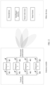
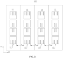
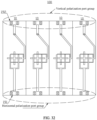
- FIG. 1 is a basic architecture of a connection relationship between an antenna module in a communication device and a baseband according to an implementation.
- FIG. 2 is a diagram in which the antenna module may cover different terminal devices according to an implementation.
- an element 1, an element 2, an element 3, and an element 4 all represent antenna elements, and ⁇ 1, ⁇ 2, ⁇ 3, and ⁇ 4 all represent phase-shift elements.
- the communication device includes the antenna module, and the antenna module is electrically connected to a baseband circuit (in FIG. 1 , the baseband represents the baseband circuit or a baseband chip) through a radio frequency channel.
- the baseband circuit transmits a radio frequency signal to the antenna module through the radio frequency channel.
- there are two radio frequency channels between the baseband circuit and the antenna module where one radio frequency channel is configured to excite horizontal polarization of the antenna module, and the other radio frequency channel is configured to excite vertical polarization of the antenna module.
- the antenna module includes an antenna array.
- the antenna array may be formed by arranging one or more antenna elements, and connection relationships between the antenna elements and the radio frequency channels are the same.
- One of the antenna elements is used as an example. One end of the antenna element is connected to one radio frequency channel through a phase-shift element, and the other end of the antenna element is connected to the other radio frequency channel through a phase-shift element.
- the antenna elements may not be connected to phase-shift elements, or some antenna elements are connected to phase-shift elements, and some antenna elements are not connected to phase-shift elements.
- the phase-shift element is configured to perform phase adjustment on a specific antenna element, to change a scanning direction of an electromagnetic wave beam of the antenna element, so that the antenna element can communicate with terminal devices at different positions.
- the four antenna elements each are connected to a phase-shift element, so that a direction of an electromagnetic wave beam of the antenna module may be varied.
- An electromagnetic wave signal of the antenna module may cover terminal devices such as a smartphone, intelligent security, a smart television, and a smart home that are distributed at different positions in a specific scenario.
- the element 1, the element 2, the element 3, and the element 4 represent four antenna elements, phase-shift elements ⁇ 1 are positioned on two sides of the element 1, phase-shift elements ⁇ 2 are positioned on two sides of the element 2, and phase-shift elements ⁇ 3 are positioned on two sides of the element 3, and phase-shift elements ⁇ 4 are positioned on two sides of the element 4.
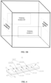
- the entire communication device is a three-dimensional columnar architecture.
- a top surface of the communication device is in a runway shape.
- the communication device includes a top area and a bottom area.
- Antenna modules are disposed in the top area.
- An antenna module I is disposed closely to the front surface of the top area, and the antenna module II is disposed closely to the back surface of the top area.
- the front surface and the back surface may be referred to by using an appearance surface of a housing of the communication device.
- the front surface is a side surface of the communication device with the housing facing a main signal environment when the communication device is in a use state
- the back surface is a side surface of the communication device with the housing being opposite to the main signal environment when the communication device is in the use state.
- a size of the communication device is small, and only one antenna module I may be disposed inside the communication device.
- the communication device is in a square box shape. Four surfaces of the communication device can radiate an electromagnetic wave signal. Four antenna modules may be disposed in the communication device.
- An antenna module I is close to a front surface
- an antenna module II is close to a left side surface
- an antenna module III is close to a back surface
- an antenna module IV is close to a right side surface.
- the front surface, the back surface, the left side surface, and the right side surface may also be referred to by using an appearance surface of a housing of the communication device. It should be understood that, that the antenna module is positioned on the front surface, the back surface, or the side surface is not limited to being positioned on an appearance surface or being disposed closely to the surface.
- FIG. 4 is a diagram of one direction of an antenna element 10 according to an implementation of this application.
- FIG. 5 is a diagram of another direction of the antenna element 10 according to the implementation of this application.
- the antenna element 10 provided in this application includes a radiation patch 12 and a feeding assembly 14, and the feeding assembly 14 is electrically connected to a radio frequency circuit in a communication device.
- the feeding assembly 14 is configured to feed the radiation patch 12.
- the feeding assembly 14 is configured to allow the radiation patch 12 to generate dual-polarized signals, for example, a horizontally polarized signal and a vertically polarized signal (hereinafter referred to as generating horizontal polarization/vertical polarization).
- two operating modes are generated during horizontal polarization feeding of the radiation patch 12, and the two operating modes are also generated during vertical polarization feeding of the radiation patch 12.
- FIG. 6 is a plane diagram of the radiation patch 12 of the antenna element according to the implementation shown in FIG. 4 .
- the radiation patch 12 includes a first additional sub-patch 1212A, a first sub-patch 1211A, a second sub-patch 1211B, and a second additional sub-patch 1212B that are sequentially arranged in a first direction A1.
- the radiation patch 12 includes a first slit 1221 and a second slit 1222 that penetrate the radiation patch 12 in a second direction A2.
- the first slit is formed between the first sub-patch 1211A and the second sub-patch 1211B.
- the second slit 1222 includes a first sub-slit 1222A and a second sub-slit 1222B.
- the first sub-slit 1222A is formed between the first sub-patch 1211A and the first additional sub-patch 1212A.
- the second sub-slit 1222B is formed between the second sub-patch 1211B and the second additional sub-patch 1212B.
- the radiation patch 12 does not have a slit that penetrates the radiation patch 12 in the first direction A1.
- An extension direction of the first slit 1221, an extension direction of the first sub-slit 1222A, and an extension direction of the second sub-slit 1222B are all the second direction A2.
- a size of the radiation patch 12 in the first direction A1 is greater than a size of the radiation patch 12 in the second direction A2.
- the first direction A1 is perpendicular to the second direction A2.
- an included angle may alternatively be formed between the first direction A1 and the second direction A2.
- the radiation patch 12 of the antenna element 10 is designed as follows: A length size in the first direction A1 is greater than a width size in the second direction A2, so that the antenna element 10 forms an elongated asymmetric structure, where the asymmetric structure means that a structure size in the first direction A1 is different from a structure size in the second direction A2, and the entire radiation patch 12 is not a square patch structure.
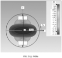
- the antenna element 10 provided in this application can generate a fan-shaped beam, implement wide coverage on a horizontal plane while maintaining a high gain, and is designed for a dual-polarized antenna.
- An overall outer profile of the radiation patch 12 is a rectangle.
- a size of the radiation patch 12 in the first direction A1 is a length of the radiation patch 12, and a size of the radiation patch 12 in the second direction A2 is a width of the radiation patch 12.
- a length-to-width ratio R of the radiation patch 12 satisfies R ⁇ 2.
- the length-to-width ratio R of the radiation patch 12 satisfies 3 ⁇ R ⁇ 5.
- the entire radiation patch 12 is a slender rectangle.
- the first slit 1221, the first sub-slit 1222A, and the second sub-slit 1222B are provided, so that the radiation patch 12 has good radiation performance in a case in which dual polarization and two operating modes of each polarization are met.
- the first additional sub-patch 1212A, the first sub-patch 1211A, the second sub-patch 1211B, and the second additional sub-patch 1212B are collectively referred to as sub-patches.
- a size of each sub-patch in the second direction A2 is a width of the sub-patch
- a size of each sub-patch in the first direction A1 is a length of the sub-patch.
- widths of all sub-patches may be equal, and lengths of all sub-patches may also be equal.
- lengths of some sub-patches in a plurality of sub-patches may alternative be different, and widths of the some patches in the plurality of sub-patches may alternative be different.
- a single sub-patch may be a rectangle or a square, or the sub-patch may be in another shape, for example, an ellipse, a trapezoid, or a polygon. This is not specifically limited in this application.
- the radiation patch 12 of the antenna element 10 has four sub-patches. In another implementation, there may alternatively be six, eight, or more sub-patches.
- the following describes a specific structure of the antenna element 10 in detail by using a specific implementation in which the radiation patch 12 has four sub-patches.
- Various limitations in this specific implementation are also applicable to other different implementations (for example, an implementation in which there may alternatively be six sub-patches).
- the radiation patch 12 includes at least three slits (namely, the first slit 1221, the first sub-slit 1222A, and the second sub-slit 1222B) that penetrate the radiation patch in the second direction A2, where a slit provided in a middle position of the radiation patch 12 in the first direction A1 is the first slit 1221, and the remaining slits are the second slit 1222.
- the radiation patch 12 is provided with three slits, including one first slit 1221 and two second slits 1222 (including the first sub-slit 1222A and the second sub-slit 1222B).
- each slit (including the first slit 1221 and the second slit 1222) includes a first end E1 and a second end E2, the first end E1 is positioned on one long edge of the radiation patch 12, the second end E2 is positioned on the other long edge of the radiation patch 12, and both the extension direction of the first slit 1221 and an extension direction of the second slit 1222 may be a direction in which the first end E1 points to the second end E2.
- the radiation patch does not have a slit that penetrates the radiation patch in the first direction, or the radiation patch has only one slit that penetrates the radiation patch in the first direction.
- the radiation patch is limited to including at least three slits that penetrate the radiation patch in the second direction, and at most one slit that penetrates the radiation patch in the first direction (which may be understood as that the radiation patch does not have a slit that penetrates the radiation patch in the first direction, or the radiation patch has only one slit that penetrates the radiation patch in the first direction), so that the antenna element 10 can be adjusted to two different operating modes (a main operating mode and a parasitic operating mode) in first polarization (for example, horizontal polarization) and two different operating modes in second polarization (for example, vertical polarization), and further the antenna element 10 can implement a dual-polarized multi-mode (at least four operating modes) state.
- a main operating mode and a parasitic operating mode in first polarization
- second polarization for example, vertical polarization
- the extension directions of the first slit 1221, the first sub-slit 1222A, and the second sub-slit 1222B are the same as extension paths, namely, the second direction A2, of the first slit 1221, the first sub-slit 1222A, and the second sub-slit 1222B.
- the first slit 1221 is used as an example.
- the first slit 1221 is a curved shape, for example, serpentine
- an extension path of the first slit 1221 is different from the extension direction of the first slit 1221, where the extension path is a curved extension track; but the extension direction is still a direction in which the first end E1 points to the second end E2, and the extension direction is still the second direction A2.
- the first slit 1221 is a curved shape, and the first sub-slit 1222A and the second sub-slit 1222B are rectangles.
- the first slit 1221 is a rectangle, and the first sub-slit 1222A and the second sub-slit 1222B are a curved shape; or the first slit 1221, the first sub-slit 1222A, and the second sub-slit 1222B may all be a curved shape.
- Extension paths of the first slit 1221, the first sub-slit 1222A, and the second sub-slit 1222B are not limited in this application.
- the extension directions of the first slit 1221, the first sub-slit 1222A, and the second sub-slit 1222B are limited to the second direction A2
- the extension paths of the first slit 1221, the first sub-slit 1222A, and the second sub-slit 1222B may be a straight line shape, a curved shape (for example, a serpentine shape or an arc shape), a sawtooth shape, or the like.
- the extension paths of the first slit 1221, the first sub-slit 1222A, and the second sub-slit 1222B are a straight line shape
- lengths of the first slit 1221, the first sub-slit 1222A, and the second sub-slit 1222B are the shortest
- the lengths of the first slit 1221, the first sub-slit 1222A, and the second sub-slit 1222B may be the width of the radiation patch 12.
- Widths of the first slit 1221, the first sub-slit 1222A, and the second sub-slit 1222B are a size perpendicular to a direction of the extension paths that are of the first slit 1221, the first sub-slit 1222A, and the second sub-slit 1222B, and the widths of the first slit 1221, the first sub-slit 1222A, and the second sub-slit 1222B may be within a range of 0.03 mm to 3 mm. In a specific implementation, a width of the slit is within a range of 0.5 mm to 1.5 mm.
- an operating frequency band and a bandwidth of the antenna element 10 may be adjusted by adjusting specific forms and widths of the first slit 1221, the first sub-slit 1222A, and the second sub-slit 1222B.
- the operating frequency band of the antenna element 10 is 5.15 GHz to 5.85 GHz.
- both a width of the first slit 1221 and a width of the second slit 1222 may be within a range of 0.03 mm to 3 mm. In an implementation, the width of the second slit 1222 is less than or equal to 2 mm.
- the width of the first slit 1221 and the width of the second slit 1222 may be the same or different. For example, the width of the first slit 1221 may be greater than the width of the second slit 1222. For example, the width of the first slit 1221 is 1.2 mm, and the width of the second slit 1222 is 0.8 mm. In an implementation, widths of all second slits 1222 are the same.
- the second slits 1222 are symmetrically distributed on two sides of the first slit 1221 in the first direction A1, and minimum spacings between the first slit 1221 and the second slits 1222 positioned on the two sides of the first slit 1221 are the same.
- the radiation patch 12 has a center line C1 extending in the second direction A2, and the radiation patch 12 is symmetrically distributed on two sides of the center line C1.
- that the first slit 1221 is in a middle position of the radiation patch 12 in a length direction may be understood as that the center line C1 is within a range covered by the first slit 1221, or the center line C1 passes through at least a part of an area of the first slit 1221.
- the center line C1 of the radiation patch 12 coincides with a center position of the first slit 1221 in a width direction.
- first slit 1221 When there are two second slits 1222, distances between the two second slits 1222 and the first slit 1221 are equal, and the two second slits 1222 are the same in size and form. When there are four or more second slits 1222, two second slits 1222 having equal distances from the first slit 1221 are the same in size and form, and second slits 1222 having different distances from the first slit 1221 may be different in size and form.
- the first additional sub-patch 1212A, the first sub-patch 1211A, the second sub-patch 1211B, and the second additional sub-patch 1212B are symmetrically distributed on the two sides of the first slit 1221 in the first direction A1.
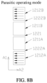
- a main operating mode and a parasitic operating mode are generated during horizontal polarization feeding of the radiation patch 12 provided in this application.
- the first sub-patch 1211A and the second sub-patch 1211B are excited to generate currents in the second direction A2, and the first sub-patch 1211A and the second sub-patch 1211B are configured to radiate electromagnetic wave signals in the main operating mode.
- a limitation on directions of the currents on the first sub-patch 1211A and the second sub-patch 1211B may be understood as follows: In the main operating mode, main currents of the first sub-patch 1211A and the second sub-patch 1211B are in the second direction A2, or the currents on the first sub-patch 1211A and the second sub-patch 1211B roughly flow in the second direction A2 from one end to the other end of the first sub-patch 1211A and from one end to the other end of the second sub-patch 1211B respectively.
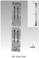
- Directions of arrow indication lines on the first sub-patch 1211A and the second sub-patch 1211B in FIG. 8A represent directions of main currents or approximate directions of currents.
- the first additional sub-patch 1212A and the second additional sub-patch 1212B are excited to generate currents in the second direction A2, and the first additional sub-patch 1212A and the second additional sub-patch 1212B are configured to radiate electromagnetic wave signals in the parasitic operating mode.
- a limitation on directions of the currents on the first additional sub-patch 1212A and the second additional sub-patch 1212B may be understood as follows: In the parasitic operating mode, main currents of the first additional sub-patch 1212A and the second additional sub-patch 1212B are in the second direction A2, or the currents on the first additional sub-patch 1212A and the second additional sub-patch 1212B roughly flow in the second direction A2 from one end to the other end of the first additional sub-patch 1212A and from one end to the other end of the second additional sub-patch 1212B respectively.
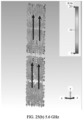
- Directions of arrow indication lines on the first additional sub-patch 1212A and the second additional sub-patch 1212B in FIG. 8B represent directions of main currents or approximate directions of currents.
- currents on the first sub-patch 1211A and the second sub-patch 1211B in the main operating mode and currents on the first additional sub-patch 1212A and the second additional sub-patch 1212B in the parasitic operating mode may be in a same direction (as shown in FIG. 8A and FIG.
- the currents are in a leftward direction or a rightward direction) or may be in opposite directions (for example, in the second direction, the currents on the first sub-patch 1211A and the second sub-patch 1211B in the main operating mode are in a leftward direction, and the currents on the first additional sub-patch 1212A and the second additional sub-patch 1212B in the parasitic operating mode are in a rightward direction).
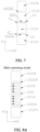
- a first operating mode and a second operating mode are generated during vertical polarization feeding of the radiation patch 12 provided in this application.
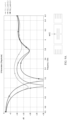
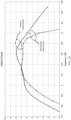
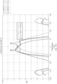
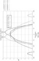
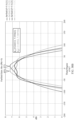
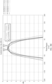
- operating frequencies of the antenna element in the first operating mode and the second operating mode may be adjusted by adjusting a width of the first slit (namely, a size of the first slit in the first direction A1) and a width of the second slit (namely, a size of the second slit in the first direction A1) respectively.
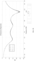
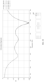
- FIG. 9A and FIG. 9B It can be seen that, when a width of a slit increases, a resonance moves toward a high frequency, where the width of the first slit (marked as ws1 in FIG. 9A ) mainly affects a resonance in the first operating mode, and the second slit (marked as ws2 in FIG. 9B ) mainly affects a resonance in the second operating mode.
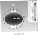
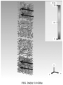
- FIG. 10A shows a current direction of the radiation patch in the first operating mode, where a straight line with an arrow that continuously extends from the bottom end of the radiation patch to a position adjacent to the top end represents the current direction.
- a current on the radiation patch 12 flows from one end to the other end of the radiation patch 12 in the first direction A1.
- FIG. 10A schematically illustrates a current direction in a state, where the current flows from the bottom end to the top end of the radiation patch 12, and positions at the bottom end and the top end may be positions of current zero points.
- FIG. 10B shows a current direction and distribution of electric fields of the radiation patch in the first operating mode.
- a straight line with an arrow that extends in a Y direction represents the current direction.
- An indication line with an arrow that extends in a Z direction represents an electric field direction and electric field strength.
- Dashed-line rectangular boxes represent the first sub-patch 1211A, the second sub-patch 1211B, the first additional sub-patch 1212A, and the second additional sub-patch 1212B respectively. Gaps between adjacent dashed-line boxes represent the first slit 1221 and the second slit 1222 respectively. Refer to FIG. 10B . In the first operating mode, an electric field generated by the antenna element 10 generates weak point reverse between the first slit 1221 and a ground plane of the feeding assembly 14.
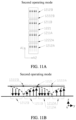
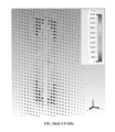
- FIG. 11A shows a current direction of the radiation patch in the second operating mode, where a straight line with an arrow that continuously extends from the bottom end of the radiation patch to a position adjacent to the top end represents the current direction.
- a current on the radiation patch 12 flows from one end to the other end of the radiation patch 12 in the first direction A1.
- FIG. 11A schematically illustrates a current direction in a state, where the current flows from the bottom end to the top end of the radiation patch 12, and positions at the bottom end and the top end may be positions of current zero points.
- FIG. 11B shows a current direction and distribution of electric fields of the radiation patch in the second operating mode.
- a straight line with an arrow that extends in a Y direction represents the current direction.
- An indication line with an arrow that extends in a Z direction represents an electric field direction and electric field strength.
- Dashed-line rectangular boxes represent the first sub-patch 1211A, the second sub-patch 1211B, the first additional sub-patch 1212A, and the second additional sub-patch 1212B respectively.
- Gaps between adjacent dashed-line boxes represent the first slit 1221 and the second slit 1222 respectively.
- FIG. 11B In the second operating mode, an electric field generated by the antenna element 10 generates strong point reverse between the second slit 1222 and a ground plane.
- the radiation patch 12 is fed by coupling a microstrip feed structure to a slit on the ground plane.
- FIG. 12 is a three-dimensional exploded view of the antenna element 10 according to this implementation of this application.
- the feeding assembly 14 includes a ground plane 15 and a feeding layer 16, the ground plane 15 is disposed between the feeding layer 16 and the radiation patch 12 in a stacked manner, and the ground plane 15 is provided with a first coupling slit 151 and a second coupling slit 152 that are provided in a cross manner.
- the ground plane 15 forms a metal grounding plane architecture on the dielectric board 11, and the first coupling slit 151 and the second coupling slit 152 are slit structures formed by removing metal materials from the ground plane 15.
- the first coupling slit 151 and the second coupling slit 152 may be filled with insulation media, and the media in the first coupling slit 151 and the second coupling slit 152 may also be air.
- an extension direction of the first coupling slit 151 is the first direction A1
- an extension direction of the second coupling slit 152 is the second direction A2
- the first coupling slit 151 and the second coupling slit 152 form a cross-shaped slit structure.
- first coupling slit 151 and the second coupling slit 152 are perpendicular to each other may be understood as that the first coupling slit 151 and the second coupling slit 152 are generally perpendicular to each other.
- the first coupling slit 151 and the second coupling slit 152 are not limited to straight-line slits in this application, provided that extension trends of the first coupling slit 151 and the second coupling slit 152 are perpendicular to each other.
- Specific shapes of the first coupling slit 151 and the second coupling slit 152 may be straight line shapes, wavy line shapes, sawtooth shapes, or the like.
- the first coupling slit 151 and the second coupling slit 152 may include slit parts in a bent form.
- a part of the first coupling slit 151 overlaps the first sub-patch 1211A, and a part of the first coupling slit 151 overlaps the second sub-patch 1211B.
- the second coupling slit 152 does not overlap the first sub-patch 1211A, and the second coupling slit 152 does not overlap the second sub-patch 1211B either.
- the second coupling slit 152 does not overlap one of the first sub-patch 1211A and the second sub-patch 1211B, and a part of the second coupling slit 152 overlaps an edge of the other one of the first sub-patch 1211A and the second sub-patch 1211B.
- the second coupling slit 152 overlaps both an edge of the first sub-patch 1211A and an edge of the second sub-patch 1211B.
- the first coupling slit 151 does not overlap neither the first additional sub-patch 1212A nor the second additional sub-patch 1212B.
- the second coupling slit 152 does not overlap neither the first additional sub-patch 1212A nor the second additional sub-patch 1212B.
- the second coupling slit 152 is provided directly opposite to the first slit 1221 on the radiation patch 12.
- “directly opposite” should be understood as that a vertical projection 152A of the second coupling slit 152 on the radiation patch 12 and the first slit 1221 are at least partially overlapped.
- "Directly opposite” described elsewhere in this document should be understood in the same or similar way.
- a width of the second coupling slit 152 is less than or equal to that of the first slit 1221, and a length of the second coupling slit 152 is greater than that of the first slit 1221.
- the vertical projection 152A of the second coupling slit 152 on the radiation patch 12 exceeds two ends of the first slit 1221 in the second direction A2. In other words, the width of the radiation patch 12 is less than the length of the second coupling slit 152. In an implementation, a center position of the second coupling slit 152 in the second direction A2 coincides with a center position of the first slit 1221 of the radiation patch 12 in the second direction A2.
- a width of the second coupling slit 152 may alternatively be greater than that of the first slit 1221, and a length of the second coupling slit 152 may alternatively be less than that of the first slit 1221.
- the second coupling slit 152 may alternatively be provided directly opposite to a sub-patch (for example, the first sub-patch 1211A or the second sub-patch 1211B) of the radiation patch 12.
- the second coupling slit 152 and the first slit 1221 may be provided in a staggered manner (that is, the second coupling slit 152 and the first slit 1221 are not provided directly opposite to each other and are not partially overlapped).
- a vertical projection 1511A of the first coupling slit 151 on the radiation patch 12 at the center position 1511 in the first direction A1 is within a range of the first sub-patch 1211A or the second sub-patch 1211B.
- the vertical projection, on the radiation patch 12, of an area in which the first coupling slit 151 intersects with the second coupling slit 152 is within a range of the first sub-patch 1211A or the second sub-patch 1211B.
- the antenna element 10 provided in an implementation of this application includes two feed units: a first feed structure and a second feed structure.
- the radiation patch 12 is fed by using the two feed units, to excite two operating modes in the horizontal polarization and two operating modes in the vertical polarization.
- a first feed structure 17 and a second feed structure 18 are disposed on the feeding layer 16.
- the first feed structure 17 is disposed directly opposite to the first coupling slit 151.
- the second feed structure 18 is disposed directly opposite to the second coupling slit 152.
- first feed structure 17 is coupled to the first coupling slit 151 to excite the horizontal polarization of the radiation patch 12
- the second feed structure 18 is coupled to the second coupling slit 152 to excite the vertical polarization of the radiation patch 12.
- the feeding layer 16 may be a two-layer metal cabling structure disposed on the dielectric board 11.
- a part of a transmission line for coupling the first feed structure 17 to the first coupling slit 151 and a part of a transmission line for coupling the second feed structure 18 to the second coupling slit 152 are distributed on different layers of the feeding layer 16; to be specific, the two parts of transmission lines are separated through some areas (which may also be a part of the dielectric board or air) of the dielectric board 11, to implement a stacking relationship in space and facilitate a small-size design of an overall feeding architecture.
- FIG. 13 is an exploded view of a layer structure of the antenna element 10.
- the antenna element 10 is successively layered into the radiation patch 12, one layer of the dielectric board 11, the ground plane 15, another layer of the dielectric board 11, a second layer 162 of the feeding layer 16, another layer of the dielectric board 11, and a first layer 161 of the feeding layer 16 from top to bottom.
- the feeding layer 16 includes the first layer 161 and the second layer 162.
- the second layer 162 is disposed between the ground plane 15 and the first layer 161 in a stacked manner.
- the ground plane 15 and the second layer 162, and the second layer 162 and the first layer 161 are respectively separated through different layers of the dielectric board 11.
- the first layer 161 may be one layer of an outer surface of the antenna element 10.
- some transmission lines of the first feed structure 17 are distributed at the first layer 161
- remaining transmission lines of the first feed structure 17 are distributed at the second layer 162
- all transmission lines of the second feed structure 18 are distributed at the first layer 161.
- the second feed structure 18 and a part of the first feed structure 17 are disposed at the first layer 161, and only a part of the first feed structure 17 is disposed at the second layer 162.
- the first feed structure 17 includes a first part 171 and a second part 172, the first part 171 is positioned at the first layer 161, the second part 172 is positioned at the second layer 162, and one end of the first part 171 is positioned at an edge of the dielectric board 11 or near an edge of the dielectric board 11.
- the first part 171 is configured to connect to a radio frequency channel through a first interface 191.
- the other end of the first part 171 passes through a via of the dielectric board 11 and is electrically connected to one end of the second part 172, and the other end of the second part 172 is coupled to the first coupling slit 151.
- all transmission lines of the first feed structure 17 may be disposed at the first layer 161
- some transmission lines of the second feed structure 18 may be disposed at the first layer 161
- remaining transmission lines of the second feed structure 18 may be disposed at the second layer 162.
- a part of the second feed structure 18 is disposed between a part of the first feed structure 17 and the ground plane 15 in a stacked manner in a thickness direction of the dielectric board 11.
- a part of the first segment 1751 is positioned on one side of the first coupling slit 151 in the second direction A2, and a part of the first segment 1751 is positioned on the other side of the first coupling slit 151 in the second direction A2.
- a part of the second segment 1752 is positioned on one side of the first coupling slit 151 in the second direction A2, and a part of the second segment 1752 is positioned on the other side of the first coupling slit 151 in the second direction A2.
- the second feed structure 18 includes a second coupling transmission line 185.
- the second coupling transmission line 185 includes a fourth segment 1851, a fifth segment 1852, and a sixth segment 1853 that are sequentially connected.
- the fourth segment 1851 and the sixth segment 1853 are spaced apart from each other.
- the fifth segment 1852 is connected between one end of the fourth segment 1851 and one end of the sixth segment 1853.
- Extension directions of the fourth segment 1851 and the sixth segment 1853 are the first direction A1.
- An extension direction of the fifth segment 1852 may be the second direction A2. Both the fourth segment 1851 and the sixth segment 1853 cross the second coupling slit 152.
- fourth segment 1851 is positioned on one side of the second coupling slit 152 in the first direction A1, and a part of the fourth segment 1851 is positioned on the other side of the second coupling slit 152 in the first direction A1.
- a part of the sixth segment 1853 is positioned on one side of the second coupling slit 152 in the first direction A1, and a part of the sixth segment 1853 is positioned on the other side of the second coupling slit 152 in the first direction A1.
- Both the first coupling transmission line 175 and the second coupling transmission line 185 may be in a ⁇ shape or a U shape.
- Relationships between a vertical projection of the first coupling transmission line 175 on the ground plane 15, and the first coupling slit 151 and the second coupling slit 152 are as follows: Vertical projections of the first segment 1751 and the third segment 1753 on the ground plane 15 intersect with the first coupling slit 151. In a specific implementation, the vertical projections of the first segment 1751 and the third segment 1753 on the ground plane are separately perpendicular to the first coupling slit 151.
- the vertical projections of the first segment 1751 and the third segment 1753 on the ground plane 15 are symmetrically distributed on two sides of the second coupling slit 152. In a specific implementation, the vertical projections of the first segment 1751 and the third segment 1753 on the ground plane 15 are parallel to the second coupling slit 152. A vertical projection of the second segment 1752 on the ground plane 15 is positioned at a periphery of the second coupling slit 152, and does not intersect with the second coupling slit 152. In a specific implementation, the vertical projection of the second segment 1752 on the ground plane 15 is parallel to the first coupling slit 151.
- Relationships between a vertical projection of the second coupling transmission line 185 on the ground plane 15, and the first coupling slit 151 and the second coupling slit 152 are as follows: Vertical projections of the fourth segment 1851 and the sixth segment 1853 on the ground plane 15 intersect with the second coupling slit 152. In a specific implementation, the vertical projections of the fourth segment 1851 and the sixth segment 1853 on the ground plane 15 are separately perpendicular to the second coupling slit 152. The vertical projections of the fourth segment 1851 and the sixth segment 1853 on the ground plane 15 are symmetrically distributed on two sides of the first coupling slit 151.
- the vertical projections of the fourth segment 1851 and the sixth segment 1853 on the ground plane 15 are parallel to the first coupling slit 151.
- a vertical projection of the fifth segment 1852 on the ground plane 15 is positioned at a periphery of the first coupling slit 151, and does not intersect with the first coupling slit 151.
- the vertical projection of the fifth segment 1852 on the ground plane 15 is parallel to the second coupling slit 152.
- the feeding assembly 14 includes the first interface 191 and the second interface 192 that are configured to connect to a radio frequency cable. Both the first interface 191 and the second interface 192 are electrically connected to a feeding network in the baseband through the radio frequency cable.
- the first interface 191 and the second interface 192 may be disposed at the first layer, so that a connection between the first interface 191 and the radio frequency cable and a connection between the second interface 192 and the radio frequency cable are more convenient, to play an advantage of easy connection.
- a radio frequency channel between the first interface 191 and the feeding network is configured to transmit a horizontally polarized radio frequency signal
- the radio frequency channel between the second interface 192 and the feeding network is configured to transmit a vertically polarized radio frequency signal.
- the first interface 191 and the second interface 192 are respectively disposed on two sides of a projection of the radiation patch 12 on the feeding layer 16, that is, the first interface 191 and the second interface 192 are distributed on two sides in the length direction of the radiation patch 12.
- the first interface 191 is used as an example to describe a specific structure.
- the first interface 191 is disposed at the first layer 161.
- the first interface 191 includes a grounding part 1911 and a conductive part 1912.
- the grounding part 1911 and the conductive part 1912 are insulated from each other.
- the grounding part 1911 includes a pair of ground pads disposed oppositely to each other.
- the conductive part 1912 may be integrally interconnected to the first feed structure 17 (or the second feed structure 18).
- the conductive part 1912 may be one end of the first feed structure 17 (or the second feed structure 18).
- the grounding part 1911 and the ground plane 15 are electrically connected, and specifically, may be electrically connected through a conductive through hole.
- An outer conductor of the radio frequency cable is welded to the grounding part 1911, and an inner conductor of the radio frequency cable is welded to the conductive part 1912.
- the grounding part 1911 and the conductive part 1912 may be separated by using air as an insulation medium.
- the first interface 191 is disposed on a periphery of the first groove 1101.
- the second interface 192 is disposed on a periphery of the second groove 1102.
- the first groove 1101 and the second groove 1102 are used to accommodate the radio frequency cable. Connectors of the radio frequency cable are accommodated in the first groove 1101 and the second groove 1102, to ensure structural flatness of a position at which the antenna element 10 is connected to the radio frequency cable, facilitate a miniaturization design of an overall size of the antenna element 10, and avoid a case in which the overall size of the antenna element 10 increases because the connector of the radio frequency cable protrudes from an outer surface of the dielectric board 11.
- the first groove 1101 and the second groove 1102 may be used to place an SMA connector.
- the radio frequency cable is electrically connected to the antenna element 10 by using the SMA connector.
- the feeding assembly 14 provided in an implementation may be a microstrip architecture disposed on the dielectric board.
- a feeding manner of the microstrip architecture helps implement size miniaturization of the antenna element 10, and helps implement a low-profile feature of the antenna element.
- the feeding assembly 14 may alternatively be in another feeding manner, for example, probe feeding.
- Both a first feed unit and a second feed unit are probe structures. The first feed unit performs feeding at one end of the radiation patch 12 in the first direction to stimulate the vertical polarization of the radiation patch, and the second feed unit performs feeding at a position that is in a middle position of the radiation patch 12 and that is adjacent to one end of the first slit 1221, to excite the horizontal polarization of the radiation patch.
- the feeding assembly 14 may be another type of feeding architecture, provided that the horizontal polarization and the vertical polarization of the radiation patch can be excited.
- the first sub-patch 1211A, the second sub-patch 1211B, the first additional sub-patch 1212A, and the second additional sub-patch 1212B are collectively referred to as sub-patches. At least one of the sub-patches is provided with a slot 1213.
- an outer profile of each sub-patch is generally a quadrilateral, for example, a square or a rectangle.
- a slot of the sub-patch should be understood as a slot extending from an outer contour edge of the sub-patch to inside of the sub-patch. It should be understood that the slot of the sub-patch may be in communication with the first slit or the second slit.
- the first sub-patch 1211A, the second sub-patch 1211B, the first additional sub-patch 1212A, and the second additional sub-patch 1212B each are provided with slots 1213.
- only one sub-patch or two symmetric sub-patches in the sub-patches may be provided with slots 1213.
- the slot 1213 extends from an edge of the sub-patch to the inside of the sub-patch.
- the slot 1213 includes a first slot and a second slot.
- the first slot is provided at a first position of the first sub-patch, and the second slot is provided at a second position of the second sub-patch.
- the first position and the second position are symmetrical with respect to the first slit 1221. It should be understood that positions of slots being "symmetrical" with respect to the first slit 1221 may not be understood as strict symmetry in a mathematical sense. In this solution, edge openings of the slots are approximately symmetrically provided on two sides of the first slit 1221, and forms of the slots are not limited to be completely consistent.
- the slot 1213 includes a third slot and a fourth slot.
- the third slot is provided at a third position of the first additional sub-patch, and the fourth slot is provided at a fourth position of the second additional sub-patch.
- the third position and the fourth position are symmetrical with respect to the first slit.
- an extension path of a current on a sub-patch with a slot increases compared with an extension path of a current on a sub-patch without a slot.
- a current length of the antenna element 10 in the first polarization (for example, the horizontal polarization) may be increased.
- the slot 1213 allows the antenna element 10 to operate at an expected frequency in the horizontal polarization in limited width space of the sub-patch.
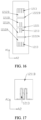
- a current flows along an edge of the sub-patch in the second direction A2. Refer to FIG. 17 .
- the slot 1213 is provided, so that the current can flow along an edge of the slot 1213.
- an extension direction of the slot 1213 includes a third direction A3.
- the third direction A3 is the same as the first direction A1.
- the extension direction of the slot 1213 may further include the first direction A1 and the second direction A2.
- the extension direction of the slot 1213 is not limited in this application, provided that the slot 1213 can increase a current direction of the antenna element 10 in the horizontal polarization, to allow the antenna element 10 to operate at an expected frequency.
- one sub-patch is provided with a plurality of (for example, two or more) slots 1213, and the plurality of slots 1213 are spaced apart from each other, so that an edge of the sub-patch is in a comb-shaped structure.
- manners (including a quantity and sizes of slots) of providing slots 1213 on the first sub-patch 1211A and the second sub-patch 1211B are the same or similar.
- the first sub-patch 1211A and the second sub-patch 1211B each are provided with two slots 1213.
- the two slots 1213 extend from edges that are of the first sub-patch 1211A and the second sub-patch 1211B and that are adjacent to the first slit 1221 to inside of the first sub-patch 1211A and inside of the second sub-patch 1211B, that is, openings of the slots 1213 on the first sub-patch 1211A and the second sub-patch 1211B face the first slit 1221.
- the slots 1213 provided on the first sub-patch 1211A and the second sub-patch 1211B are symmetrical with respect to the first slit 1221.
- Manners including a quantity and sizes of slots 1213 of providing slots 1213 on the first additional sub-patch 1212A and the second additional sub-patch 1212B are the same or similar.
- the first additional sub-patch 1212A and the second additional sub-patch 1212B each are provided with four slots 1213.
- the four slots 1213 extend from edges that are of the first additional sub-patch 1212A and the second additional sub-patch 1212B and that are away from the first sub-patch 1211A and the second sub-patch 1211B to inside of the first additional sub-patch 1212A and inside of the second additional sub-patch 1212B, that is, openings of the slots 1213 on the first additional sub-patch 1212A and the second additional sub-patch 1212B are positioned at a top edge or a bottom edge of the radiation patch 12.
- the slots 1213 provided on the first additional sub-patch 1212A and the second additional sub-patch 1212B are symmetrical with respect to the first slit 1221.
- a sub-patch arranged at the head or tail of a row of sub-patches of the radiation patch 12 is an edge patch.
- the first additional sub-patch 1212A and the second additional sub-patch 1212B are edge patches.
- the first additional sub-patch 1212A and the second additional sub-patch 1212B each include a patch body 1214 and protruding structures 1215 connected to the patch body 1214.
- the protruding structures 1215 are positioned on a side that is of the patch body 1214 and that is away from the first sub-patch 1211A and the second sub-patch 1211B, and an extension direction of the protruding structures 1215 includes the third direction A3.
- the third direction A3 is the same as the first direction A1, or there is an included angle between the third direction A3 and the first direction A1.
- a principle of disposing the protruding structure 1215 is the same as or similar to a design principle of the slot 1213.
- the protruding structure 1215 is disposed at an edge of the edge patch, so that a path of a current flow direction of the antenna element 10 in the horizontal polarization changes, and a current path becomes longer, to adjust a frequency.
- a shape of the protruding structure 1215 may be a rectangle or a triangle. If another shape is used, an edge of the protruding structure 1215 may be a straight-line edge, or may include a curved edge or an arc edge.
- FIG. 27 , FIG. 28 , FIG. 29 , and FIG. 30 are respective diagrams of S-parameters of the horizontal polarization port and the vertical polarization port during excitation when slots extending in the third direction have different sizes.
- FIG. 27 shows impact of adjusting a size, namely, Ld1, of a slot on the first sub-patch on a main mode and a parasitic mode that are generated when the antenna element is horizontally polarized.
- a slot or protruding structure is provided on a sub-patch, so that a frequency response of a horizontal polarization port can be independently controlled; and a dual-polarized symmetric slot or protruding structure is designed, so that resonance frequencies in the main operating mode and the parasitic operating mode during horizontal polarization feeding can be separately adjusted.
- a direction of the slot is the first direction, and the slot does not affect distribution of currents in the vertical polarization. Therefore, the slot does not affect an operating frequency in the vertical polarization.
- the antenna array provided in this application includes at least two antenna elements, and the at least two antenna elements are sequentially arranged in the second direction.
- the antenna array provided in this application is a low-profile dual-polarized array. Refer to FIG. 31 .
- a physical length of the spacing d between the adjacent antenna elements 10 varies greatly depending on a frequency band range. In a 5G Wi-Fi frequency band, the physical length of the spacing d between the adjacent antenna elements 10 ranges from 10 mm to 42 mm.
- First interfaces 191 of all antenna elements 10 are positioned on one edge of the antenna array 100, and second interfaces 192 of all antenna elements 10 are positioned on the other edge of the antenna array 100.
- the four antenna elements 10 have eight feeding ports (which are four first interfaces 191 and four second interfaces 192 respectively), the four first interfaces 191 are arranged at a first edge position (for example, a bottom edge in the figure) of the antenna array 100, and the four second interfaces 192 are arranged at a second edge position (for example, a top edge in the figure) of the antenna array 100.
- This design facilitates cable connection.
- feeding ports of adjacent antenna elements are isolated from each other, for example, horizontal polarization feeding ports or vertical polarization feeding ports are isolated from each other at an equal or similar spacing, to facilitate circuit configuration and ensure consistency of electromagnetic wave signal beams.
- the antenna array 100 may be connected to the phase-shift element.
- the phase-shift element For a specific connection manner, refer to FIG. 1 (described above, and details are not described again).
- FIG. 33 is a diagram of a situation in which an array factor in an antenna array (which may be a one-dimensional linear array) including four antenna elements changes with a spacing d between the antenna elements.
- a specific spacing d between the antenna elements that is marked in the upper right corner of the curve graph as FIG. 33 points to a specific curve by using an indication line with an arrow. It can be seen from FIG.
- FIG. 34 is an architecture of an antenna array of a patch 1*4 array.
- the antenna array 100A includes four antenna elements 10A.
- FIG. 35 shows a situation in which an array gain of a patch 1*4 array changes with a spacing between elements.
- FIG. 36 shows a situation in which an array gain of a low-profile high-performance dual-polarized 1*4 antenna array changes with a spacing between elements according to this application.
- Beam widening may be understood as a width of a horizontal coordinate in a peak area of a main lobe corresponding to a same vertical coordinate.
- FIG. 37A to FIG. 37C are diagrams of beam consistency of a patch 1*4 array at different spacings (namely, spacings d between antenna elements are ⁇ /4, ⁇ /3, and ⁇ /2 respectively).
- FIG. 38A to FIG. 38C are diagrams of beam consistency of a low-profile high-performance dual-polarized 1*4 antenna array at different spacings (namely, spacings d between antenna elements are ⁇ /4, ⁇ /3, and ⁇ /2 respectively) according to this application. It can be learned by comparing FIG. 37A to FIG. 37C with FIG. 38A to FIG.
- beam consistency of antenna elements of the low-profile high-performance dual-polarized 1*4 antenna array provided in this application is greatly better than that of the patch 1*4 array antenna. Beam consistency may be reflected through peak value distribution. A distance between peak values of beams shown in FIG. 37A to FIG. 37C is large, and a distance between peak values of corresponding beams shown in FIG. 38A to FIG. 38C is small.
- FIG. 39(a) to FIG. 39(c) are diagrams of S-parameters of an antenna array according to a specific implementation of this application.
- an operating bandwidth of the antenna array provided in this application in the vertical polarization may cover 5.1 GHz to 5.9 GHz, and in-band isolation between each port is greater than 13.2 dB.
- An operating bandwidth in the horizontal polarization may cover 5.1 GHz to 5.8 GHz, and in-band isolation between each port is greater than 10.4 dB.
- the in-band isolation between the horizontal polarization and the vertical polarization is higher than 16.6 dB. This indicates that the antenna array provided in this application has good bandwidth and isolation performance when the antenna array is arranged at a small spacing.
- FIG. 40(a) and FIG. 40(b) are diagrams of scanning capabilities of the antenna array in the horizontal polarization and the vertical polarization at 5.2 GHz, 5.5 GHz, and 5.8 GHz according to a specific implementation of this application. As shown in FIG. 40(a) and FIG.
- scanning angles of 3 dB gain roll-off at 5.2 GHz, 5.5 GHz, and 5.8 GHz in the vertical polarization are 70°, 69°, and 66°, respectively
- scanning angles of 5 dB gain roll-off at 5.2 GHz, 5.5 GHz, and 5.8 GHz in the vertical polarization are 85°, 81°, and 78°, respectively
- scanning angles of 3 dB gain roll-off at 5.2 GHz, 5.5 GHz, and 5.8 GHz in the horizontal polarization are 71°, 67°, and 66°, respectively
- scanning angles of 5 dB gain roll-off at 5.2 GHz, 5.5 GHz, and 5.8 GHz in the horizontal polarization are 81°, 80°, and 79°, respectively.
- Table 1 and Table 2 respectively show scanning performance and a phase requirement of an antenna array provided in an implementation of this application in the vertical polarization and the horizontal polarization. It can be learned from the tables that both the vertical polarization and the horizontal polarization show good gain levels and scanning/coverage performance, gain and scanning performance of the vertical polarization are slightly better than those of horizontal polarization. States in status bars in Table 1 and Table 2 is a phase difference between two adjacent feeding ports.
- Table 1 reflects a phase difference between two adjacent feeding ports in a vertical polarization port group, where a state I indicates that all feeding ports have a same phase, that is, a phase difference between two adjacent feeding ports is 0°; a state II indicates that a phase difference between two adjacent feeding ports is 45°; and a state III indicates that a phase difference between two adjacent feeding ports is 120°.
- FIG. 1 indicates that a phase difference between two adjacent feeding ports in a vertical polarization port group, where a state I indicates that all feeding ports have a same phase, that is, a phase difference between two adjacent feeding ports is 0°; a state II indicates that a phase difference between two adjacent feeding ports is 45°; and a state III indicates that a phase difference between two adjacent feeding ports is 120°.
- FIG. 1 reflects a phase difference between two adjacent feeding ports in a vertical polarization port group, where a state I indicates that all feeding ports have a same phase, that is, a phase difference between two adjacent feeding ports is 0°; a
- a state I indicates that all feeding ports have a same phase, that is, a phase difference between two adjacent feeding ports is 0°; a state II indicates that a phase difference between two adjacent feeding ports is 45°; and a state III indicates that a phase difference between two adjacent feeding ports is 120°.
- Table 1 Scanning performance and phase requirements of the array in the vertical polarization Vertical polarization Frequency (GHz) Isolation (dB) Peak gain (dBi) Scanning angle (3 dB gain drop) Scanning angle (5 dB gain drop) Status Phase Beam direction Gain (dBi) 5.2 13.3 10.9 70 85 State I 0° 0° 10.9 State II 45° 27° 10.7 State III 120° 52° 9.2 5.5 14.4 11.5 69 81 State I 0° 0° 11.5 State II 45° 24° 11.2 State III 120° 53° 9.5 5.8 13.2 12.0 66 78 State I 0° 0° 12.0 State II 45° 23° 11.7 State III 120° 50° 10.1 Table 2 Scanning performance and phase requirements of the array in the horizontal polarization Horizontal polarization Frequency (GHz) Isolation (dB) Peak gain (dBi) Scanning angle (3 dB gain drop) Scanning angle (5 dB gain drop) Status Phase Beam direction Gain (d
Landscapes
- Physics & Mathematics (AREA)
- Electromagnetism (AREA)
- Waveguide Aerials (AREA)
- Variable-Direction Aerials And Aerial Arrays (AREA)
Applications Claiming Priority (2)
| Application Number | Priority Date | Filing Date | Title |
|---|---|---|---|
| CN202211147258.5A CN117766989A (zh) | 2022-09-19 | 2022-09-19 | 天线单元、天线阵列和通信设备 |
| PCT/CN2023/119355 WO2024061154A1 (zh) | 2022-09-19 | 2023-09-18 | 天线单元、天线阵列和通信设备 |
Publications (2)
| Publication Number | Publication Date |
|---|---|
| EP4521555A1 true EP4521555A1 (de) | 2025-03-12 |
| EP4521555A4 EP4521555A4 (de) | 2025-08-13 |
Family
ID=90324424
Family Applications (1)
| Application Number | Title | Priority Date | Filing Date |
|---|---|---|---|
| EP23867443.6A Pending EP4521555A4 (de) | 2022-09-19 | 2023-09-18 | Antenneneinheit, antennenanordnung und kommunikationsvorrichtung |
Country Status (3)
| Country | Link |
|---|---|
| EP (1) | EP4521555A4 (de) |
| CN (1) | CN117766989A (de) |
| WO (1) | WO2024061154A1 (de) |
Families Citing this family (1)
| Publication number | Priority date | Publication date | Assignee | Title |
|---|---|---|---|---|
| CN119921114B (zh) * | 2025-04-03 | 2025-06-24 | 成都频岢微电子有限公司 | 一种基于奇偶模原理的共口径高增益方向图可重构天线 |
Family Cites Families (8)
| Publication number | Priority date | Publication date | Assignee | Title |
|---|---|---|---|---|
| GB9002636D0 (en) * | 1990-02-06 | 1990-04-04 | British Telecomm | Antenna |
| US20180123245A1 (en) * | 2016-10-28 | 2018-05-03 | Broadcom Corporation | Broadband antenna array for wireless communications |
| CN107394378A (zh) * | 2017-07-13 | 2017-11-24 | 清华大学 | 采用网格状辐射贴片的宽带低剖面双极化微带天线 |
| CN114122682A (zh) * | 2020-08-25 | 2022-03-01 | 华为技术有限公司 | 天线单元、天线阵列及电子设备 |
| CN114976583B (zh) * | 2021-02-26 | 2023-12-15 | 华为技术有限公司 | 毫米波天线、装置及电子设备 |
| CN113097726B (zh) * | 2021-04-07 | 2023-03-10 | 广东工业大学 | 一种双频双圆极化微带天线 |
| CN113629398B (zh) * | 2021-10-12 | 2022-02-08 | 深圳大学 | 一种具有一致辐射方向图且增益提高的宽带耦合贴片天线 |
| US12334637B2 (en) * | 2022-03-07 | 2025-06-17 | Tyco Electronics Holdings (Bermuda) No. 7 Limited | Metasurface antenna |
-
2022
- 2022-09-19 CN CN202211147258.5A patent/CN117766989A/zh active Pending
-
2023
- 2023-09-18 EP EP23867443.6A patent/EP4521555A4/de active Pending
- 2023-09-18 WO PCT/CN2023/119355 patent/WO2024061154A1/zh not_active Ceased
Also Published As
| Publication number | Publication date |
|---|---|
| CN117766989A (zh) | 2024-03-26 |
| EP4521555A4 (de) | 2025-08-13 |
| WO2024061154A1 (zh) | 2024-03-28 |
Similar Documents
| Publication | Publication Date | Title |
|---|---|---|
| US11387568B2 (en) | Millimeter-wave antenna array element, array antenna, and communications product | |
| US9698487B2 (en) | Array antenna | |
| US9401545B2 (en) | Multi polarization conformal channel monopole antenna | |
| AU2011354510B2 (en) | Antenna having external and internal structures | |
| JP5388943B2 (ja) | 導波管・msl変換器及び平面アンテナ | |
| US20190305415A1 (en) | Integrated multi-standard antenna system with dual function connected array | |
| JP3923360B2 (ja) | スロットアレーアンテナ及びスロットアレーアンテナ装置 | |
| CN114374085A (zh) | 一种面向5g毫米波双频段应用的双极化混合天线 | |
| WO2022042231A1 (zh) | 天线单元、天线阵列及电子设备 | |
| CN106340711B (zh) | 双极化天线 | |
| WO2021148858A1 (en) | A magneto-electric dipole antenna | |
| US6967624B1 (en) | Wideband antenna element and array thereof | |
| CN113497357B (zh) | 一种宽带双极化滤波天线 | |
| EP4521555A1 (de) | Antenneneinheit, antennenanordnung und kommunikationsvorrichtung | |
| CN114883805B (zh) | 一种具有前后比抑制的小型化天线单元及其阵列 | |
| WO2022135238A1 (en) | Dual-polarized substrate-integrated 360° beam steering antenna | |
| JP3514305B2 (ja) | チップアンテナ | |
| TWI451632B (zh) | 高增益迴圈陣列天線系統及電子裝置 | |
| CN220492202U (zh) | 一种应用于x频段的宽带端射天线 | |
| CN215418582U (zh) | 天线 | |
| CN118487053A (zh) | 天线结构及电子设备 | |
| CN117638466A (zh) | 天线模组、天线阵列及电子设备 | |
| CN114843749A (zh) | 天线、探测装置、雷达及终端 | |
| CN116683171B (zh) | 一种应用于x频段的宽带端射天线 | |
| CN116683173B (zh) | 一种单层小型化双频定位天线 |
Legal Events
| Date | Code | Title | Description |
|---|---|---|---|
| STAA | Information on the status of an ep patent application or granted ep patent |
Free format text: STATUS: THE INTERNATIONAL PUBLICATION HAS BEEN MADE |
|
| PUAI | Public reference made under article 153(3) epc to a published international application that has entered the european phase |
Free format text: ORIGINAL CODE: 0009012 |
|
| STAA | Information on the status of an ep patent application or granted ep patent |
Free format text: STATUS: REQUEST FOR EXAMINATION WAS MADE |
|
| 17P | Request for examination filed |
Effective date: 20241205 |
|
| AK | Designated contracting states |
Kind code of ref document: A1 Designated state(s): AL AT BE BG CH CY CZ DE DK EE ES FI FR GB GR HR HU IE IS IT LI LT LU LV MC ME MK MT NL NO PL PT RO RS SE SI SK SM TR |
|
| REG | Reference to a national code |
Ref country code: DE Ref legal event code: R079 Free format text: PREVIOUS MAIN CLASS: H01Q0001380000 Ipc: H01Q0005342000 |
|
| A4 | Supplementary search report drawn up and despatched |
Effective date: 20250715 |
|
| RIC1 | Information provided on ipc code assigned before grant |
Ipc: H01Q 5/342 20150101AFI20250709BHEP Ipc: H01Q 5/385 20150101ALI20250709BHEP Ipc: H01Q 9/04 20060101ALI20250709BHEP Ipc: H01Q 19/00 20060101ALI20250709BHEP Ipc: H01Q 21/08 20060101ALI20250709BHEP Ipc: H01Q 21/24 20060101ALI20250709BHEP |
|
| DAV | Request for validation of the european patent (deleted) | ||
| DAX | Request for extension of the european patent (deleted) |