EP4521858A1 - Dispositif électronique comprenant une carte de circuit imprimé souple - Google Patents
Dispositif électronique comprenant une carte de circuit imprimé souple Download PDFInfo
- Publication number
- EP4521858A1 EP4521858A1 EP24772196.2A EP24772196A EP4521858A1 EP 4521858 A1 EP4521858 A1 EP 4521858A1 EP 24772196 A EP24772196 A EP 24772196A EP 4521858 A1 EP4521858 A1 EP 4521858A1
- Authority
- EP
- European Patent Office
- Prior art keywords
- electronic device
- circuit board
- printed circuit
- flexible printed
- antenna
- Prior art date
- Legal status (The legal status is an assumption and is not a legal conclusion. Google has not performed a legal analysis and makes no representation as to the accuracy of the status listed.)
- Pending
Links
Images






Classifications
-
- H—ELECTRICITY
- H01—ELECTRIC ELEMENTS
- H01R—ELECTRICALLY-CONDUCTIVE CONNECTIONS; STRUCTURAL ASSOCIATIONS OF A PLURALITY OF MUTUALLY-INSULATED ELECTRICAL CONNECTING ELEMENTS; COUPLING DEVICES; CURRENT COLLECTORS
- H01R12/00—Structural associations of a plurality of mutually-insulated electrical connecting elements, specially adapted for printed circuits, e.g. printed circuit boards [PCB], flat or ribbon cables, or like generally planar structures, e.g. terminal strips, terminal blocks; Coupling devices specially adapted for printed circuits, flat or ribbon cables, or like generally planar structures; Terminals specially adapted for contact with, or insertion into, printed circuits, flat or ribbon cables, or like generally planar structures
- H01R12/50—Fixed connections
- H01R12/59—Fixed connections for flexible printed circuits, flat or ribbon cables or like structures
- H01R12/65—Fixed connections for flexible printed circuits, flat or ribbon cables or like structures characterised by the terminal
-
- H—ELECTRICITY
- H01—ELECTRIC ELEMENTS
- H01Q—ANTENNAS, i.e. RADIO AERIALS
- H01Q1/00—Details of, or arrangements associated with, antennas
- H01Q1/12—Supports; Mounting means
- H01Q1/22—Supports; Mounting means by structural association with other equipment or articles
- H01Q1/24—Supports; Mounting means by structural association with other equipment or articles with receiving set
- H01Q1/241—Supports; Mounting means by structural association with other equipment or articles with receiving set used in mobile communications, e.g. GSM
- H01Q1/242—Supports; Mounting means by structural association with other equipment or articles with receiving set used in mobile communications, e.g. GSM specially adapted for hand-held use
- H01Q1/243—Supports; Mounting means by structural association with other equipment or articles with receiving set used in mobile communications, e.g. GSM specially adapted for hand-held use with built-in antennas
-
- H—ELECTRICITY
- H04—ELECTRIC COMMUNICATION TECHNIQUE
- H04M—TELEPHONIC COMMUNICATION
- H04M1/00—Substation equipment, e.g. for use by subscribers
- H04M1/02—Constructional features of telephone sets
- H04M1/0202—Portable telephone sets, e.g. cordless phones, mobile phones or bar type handsets
- H04M1/026—Details of the structure or mounting of specific components
-
- H—ELECTRICITY
- H05—ELECTRIC TECHNIQUES NOT OTHERWISE PROVIDED FOR
- H05K—PRINTED CIRCUITS; CASINGS OR CONSTRUCTIONAL DETAILS OF ELECTRIC APPARATUS; MANUFACTURE OF ASSEMBLAGES OF ELECTRICAL COMPONENTS
- H05K1/00—Printed circuits
- H05K1/18—Printed circuits structurally associated with non-printed electric components
- H05K1/189—Printed circuits structurally associated with non-printed electric components characterised by the use of flexible or folded printed circuits
-
- H—ELECTRICITY
- H01—ELECTRIC ELEMENTS
- H01R—ELECTRICALLY-CONDUCTIVE CONNECTIONS; STRUCTURAL ASSOCIATIONS OF A PLURALITY OF MUTUALLY-INSULATED ELECTRICAL CONNECTING ELEMENTS; COUPLING DEVICES; CURRENT COLLECTORS
- H01R12/00—Structural associations of a plurality of mutually-insulated electrical connecting elements, specially adapted for printed circuits, e.g. printed circuit boards [PCB], flat or ribbon cables, or like generally planar structures, e.g. terminal strips, terminal blocks; Coupling devices specially adapted for printed circuits, flat or ribbon cables, or like generally planar structures; Terminals specially adapted for contact with, or insertion into, printed circuits, flat or ribbon cables, or like generally planar structures
- H01R12/50—Fixed connections
- H01R12/59—Fixed connections for flexible printed circuits, flat or ribbon cables or like structures
- H01R12/62—Fixed connections for flexible printed circuits, flat or ribbon cables or like structures connecting to rigid printed circuits or like structures
-
- H—ELECTRICITY
- H01—ELECTRIC ELEMENTS
- H01R—ELECTRICALLY-CONDUCTIVE CONNECTIONS; STRUCTURAL ASSOCIATIONS OF A PLURALITY OF MUTUALLY-INSULATED ELECTRICAL CONNECTING ELEMENTS; COUPLING DEVICES; CURRENT COLLECTORS
- H01R13/00—Details of coupling devices of the kinds covered by groups H01R12/70 or H01R24/00 - H01R33/00
- H01R13/02—Contact members
- H01R13/22—Contacts for co-operating by abutting
- H01R13/24—Contacts for co-operating by abutting resilient; resiliently-mounted
- H01R13/2442—Contacts for co-operating by abutting resilient; resiliently-mounted with a single cantilevered beam
-
- H—ELECTRICITY
- H01—ELECTRIC ELEMENTS
- H01R—ELECTRICALLY-CONDUCTIVE CONNECTIONS; STRUCTURAL ASSOCIATIONS OF A PLURALITY OF MUTUALLY-INSULATED ELECTRICAL CONNECTING ELEMENTS; COUPLING DEVICES; CURRENT COLLECTORS
- H01R2201/00—Connectors or connections adapted for particular applications
- H01R2201/02—Connectors or connections adapted for particular applications for antennas
-
- H—ELECTRICITY
- H04—ELECTRIC COMMUNICATION TECHNIQUE
- H04M—TELEPHONIC COMMUNICATION
- H04M1/00—Substation equipment, e.g. for use by subscribers
- H04M1/02—Constructional features of telephone sets
- H04M1/0202—Portable telephone sets, e.g. cordless phones, mobile phones or bar type handsets
- H04M1/026—Details of the structure or mounting of specific components
- H04M1/0264—Details of the structure or mounting of specific components for a camera module assembly
-
- H—ELECTRICITY
- H05—ELECTRIC TECHNIQUES NOT OTHERWISE PROVIDED FOR
- H05K—PRINTED CIRCUITS; CASINGS OR CONSTRUCTIONAL DETAILS OF ELECTRIC APPARATUS; MANUFACTURE OF ASSEMBLAGES OF ELECTRICAL COMPONENTS
- H05K2201/00—Indexing scheme relating to printed circuits covered by H05K1/00
- H05K2201/10—Details of components or other objects attached to or integrated in a printed circuit board
- H05K2201/10007—Types of components
- H05K2201/10121—Optical component, e.g. opto-electronic component
-
- H—ELECTRICITY
- H05—ELECTRIC TECHNIQUES NOT OTHERWISE PROVIDED FOR
- H05K—PRINTED CIRCUITS; CASINGS OR CONSTRUCTIONAL DETAILS OF ELECTRIC APPARATUS; MANUFACTURE OF ASSEMBLAGES OF ELECTRICAL COMPONENTS
- H05K2201/00—Indexing scheme relating to printed circuits covered by H05K1/00
- H05K2201/10—Details of components or other objects attached to or integrated in a printed circuit board
- H05K2201/10007—Types of components
- H05K2201/10151—Sensor
Definitions
- Various embodiments disclosed herein relate to an electronic device and, more specifically, to an electronic device including a flexible printed circuit board.
- An electronic device may include a conducting wire configured to transmit a signal or supply power. Inside the electronic device, the conducting wire may exist, for example, in the form of a cable and/or wiring on a circuit board.
- the electronic device may include a flat cable (for example, a flexible flat cable (FFC) implemented as a flexible printed circuit board (FPCB)) in order to minimize a size (for example, a thickness) of the electronic device.
- FFC flexible flat cable
- FPCB flexible printed circuit board
- the electronic device may include an antenna for wireless communication and a wireless communication module configured to perform a communication operation in a radio frequency band through the antenna.
- the wireless communication module and the antenna may be connected to each other by the above-described conducting wire (for example, a flexible circuit board).
- a contact terminal is disposed at a distal end of the conducting wire, and the contact terminal and the antenna are in contact with each other, so that the antenna and the wireless communication module are electrically connected to each other by the conducting wire.
- Various embodiments disclosed herein may provide an electronic device which has an improved electrical connection between a communication module and an antenna and more efficiently uses an internal space of the electronic device.
- An electronic device may include: a frame including at least one antenna and having a metal material and a polymer material; a front plate coupled to the frame; a rear plate coupled to the frame in an opposite direction to the front plate; at least one electrical component at least partially disposed in an internal space defined by the frame, the front plate, and the rear plate; a printed circuit board disposed in the internal space; a flexible printed circuit board having a first end portion electrically connected to the printed circuit board and a second end portion extending to be adjacent to the at least one antenna; and a contact member which is disposed in the other end portion of the flexible printed circuit board, in electrical contact with the at least one antenna, and oriented to apply an elastic force in a direction parallel to a surface of the flexible printed circuit board.
- the flexible printed circuit board may extend along one surface of the electrical component within the internal space and include a protrusion portion formed by increasing a width of the flexible printed circuit board in an area adjacent to the other end portion.
- the protrusion portion restricts, reduces or prevents a movement of the flexible printed circuit board when a reaction force acts on the flexible printed circuit board.
- the flexible printed circuit board therefore remains in substantially a same position, so an electrical contact of the contact member with the at least one antenna is not degraded, or is only minimally degraded.
- the electrical contact of the contact member with the at least one antenna is therefore better when the electronic device comprises a protrusion portion, compared with electronic devices which do not comprise the protrusion portion.
- the frame may include: a lateral frame positioned on a lateral surface of the electronic device and including a plurality of metal segments and a polymer injection portion coupled to the metal segments; and a support member coupled to the lateral frame and extending from the lateral frame into an inside of the electronic device, wherein the at least one antenna is at least one of the plurality of metal segments.
- the flexible printed circuit board may extend through a portion between the support member and the one surface of the electrical component.
- the support member may include a catching protrusion formed to allow the protrusion portion to be caught thereby in an area of the support member corresponding to the protrusion portion.
- the electronic device may include a fixing member positioned in a first direction perpendicular to the surface of the flexible printed circuit board from the contact member and configured to fix the contact member with respect to the first direction.
- the contact member contacts with the at least one antenna, and the protrusion portion prevents or reduces a movement of the flexible printed circuit board caused by a reaction force of the contacting
- the flexible printed circuit board may flex, bend or move in a direction perpendicular to a direction of the reaction force (and therefore perpendicular to the surface of the flexible printed circuit board.
- the fixing member prevents this movement of the flexible circuit board in the direction perpendicular to the surface of the flexible printed circuit board.
- the flexible circuit board therefore remains at least substantially in a same position, so the electrical contacts of the flexible circuit board with other components of the electronic device remain stable.
- the electrical component may include a flange extending to be positioned in the first direction with respect to the fixing member, and the flange may fix the fixing member with respect to the first direction.
- the fixing member may include a flange groove having a shape corresponding to the flange, and the flange may be inserted into the flange groove.
- the lateral frame may include a fixing groove formed in an area where the contact member is in contact with the at least one antenna and having a shape at least partially corresponding to the fixing member, and the fixing member may be fixed by being inserted into the fixing groove.
- a dimension of the fixing member may be configured so that the fixing member is fixedly fitted through an interference fit in an inner surface of the fixing groove.
- the fixing groove may be formed by partially removing the polymer material to expose a surface of the antenna facing an inside of the electronic device in an area where the contact member is in contact with the at least one antenna, and the fixing member may be configured to reinforce rigidity of the area where the polymer material has been partially removed by interference-fitting the fixing member to an inner surface of the fixing groove.
- the flexible printed circuit board may extend through a portion between the rear plate and one surface of the electrical component facing the rear plate.
- the processor 120 may include a main processor 121 (e.g., a central processing unit (CPU) or an application processor (AP)), or an auxiliary processor 123 (e.g., a graphics processing unit (GPU), a neural processing unit (NPU), an image signal processor (ISP), a sensor hub processor, or a communication processor (CP)) that is operable independently from, or in conjunction with, the main processor 121.
- a main processor 121 e.g., a central processing unit (CPU) or an application processor (AP)
- auxiliary processor 123 e.g., a graphics processing unit (GPU), a neural processing unit (NPU), an image signal processor (ISP), a sensor hub processor, or a communication processor (CP)
- the main processor 121 may be adapted to consume less power than the main processor 121, or to be specific to a specified function.
- the auxiliary processor 123 may be implemented as separate from, or as part of the main processor 121.
- the memory 130 may store various data used by at least one component (e.g., the processor 120 or the sensor module 176) of the electronic device 101.
- the various data may include, for example, software (e.g., the program 140) and input data or output data for a command related thererto.
- the memory 130 may include the volatile memory 132 or the non-volatile memory 134.
- the sensor module 176 may detect an operational state (e.g., power or temperature) of the electronic device 101 or an environmental state (e.g., a state of a user) external to the electronic device 101, and then generate an electrical signal or data value corresponding to the detected state.
- the sensor module 176 may include, for example, a gesture sensor, a gyro sensor, an atmospheric pressure sensor, a magnetic sensor, an acceleration sensor, a grip sensor, a proximity sensor, a color sensor, an infrared (IR) sensor, a biometric sensor, a temperature sensor, a humidity sensor, or an illuminance sensor.
- the interface 177 may support one or more specified protocols to be used for the electronic device 101 to be coupled with the external electronic device (e.g., the electronic device 102) directly (e.g., wiredly) or wirelessly.
- the interface 177 may include, for example, a high definition multimedia interface (HDMI), a universal serial bus (USB) interface, a secure digital (SD) card interface, or an audio interface.
- HDMI high definition multimedia interface
- USB universal serial bus
- SD secure digital
- a connecting terminal 178 may include a connector via which the electronic device 101 may be physically connected with the external electronic device (e.g., the electronic device 102).
- the connecting terminal 178 may include, for example, a HDMI connector, a USB connector, a SD card connector, or an audio connector (e.g., a headphone connector).
- the camera module 180 may capture a still image or moving images.
- the camera module 180 may include one or more lenses, image sensors, image signal processors, or flashes.
- the power management module 188 may manage power supplied to the electronic device 101.
- the power management module 188 may be implemented as at least part of, for example, a power management integrated circuit (PMIC).
- PMIC power management integrated circuit
- the communication module 190 may include a wireless communication module 192 (e.g., a cellular communication module, a short-range wireless communication module, or a global navigation satellite system (GNSS) communication module) or a wired communication module 194 (e.g., a local area network (LAN) communication module or a power line communication (PLC) module).
- a wireless communication module 192 e.g., a cellular communication module, a short-range wireless communication module, or a global navigation satellite system (GNSS) communication module
- GNSS global navigation satellite system
- wired communication module 194 e.g., a local area network (LAN) communication module or a power line communication (PLC) module.
- LAN local area network
- PLC power line communication
- a corresponding one of these communication modules may communicate with the external electronic device via the first network 198 (e.g., a short-range communication network, such as BluetoothTM, wireless-fidelity (Wi-Fi) direct, or infrared data association (IrDA)) or the second network 199 (e.g., a long-range communication network, such as a legacy cellular network, a 5G network, a next-generation communication network, the Internet, or a computer network (e.g., LAN or wide area network (WAN)).
- first network 198 e.g., a short-range communication network, such as BluetoothTM, wireless-fidelity (Wi-Fi) direct, or infrared data association (IrDA)
- the second network 199 e.g., a long-range communication network, such as a legacy cellular network, a 5G network, a next-generation communication network, the Internet, or a computer network (e.g., LAN or wide area network (WAN)).
- the wireless communication module 192 may identify and authenticate the electronic device 101 in a communication network, such as the first network 198 or the second network 199, using subscriber information (e.g., international mobile subscriber identity (IMSI)) stored in the subscriber identification module 196.
- subscriber information e.g., international mobile subscriber identity (IMSI)
- the wireless communication module 192 may support a peak data rate (e.g., 20Gbps or more) for implementing eMBB, loss coverage (e.g., 164dB or less) for implementing mMTC, or U-plane latency (e.g., 0.5ms or less for each of downlink (DL) and uplink (UL), or a round trip of 1ms or less) for implementing URLLC.
- a peak data rate e.g., 20Gbps or more
- loss coverage e.g., 164dB or less
- U-plane latency e.g., 0.5ms or less for each of downlink (DL) and uplink (UL), or a round trip of 1ms or less
- the antenna module 197 may transmit or receive a signal or power to or from the outside (e.g., the external electronic device) of the electronic device 101.
- the antenna module 197 may include an antenna including a radiating element composed of a conductive material or a conductive pattern formed in or on a substrate (e.g., a printed circuit board (PCB)).
- the antenna module 197 may include a plurality of antennas (e.g., array antennas). In such a case, at least one antenna appropriate for a communication scheme used in the communication network, such as the first network 198 or the second network 199, may be selected, for example, by the communication module 190 (e.g., the wireless communication module 192) from the plurality of antennas.
- the signal or the power may then be transmitted or received between the communication module 190 and the external electronic device via the selected at least one antenna.
- another component e.g., a radio frequency integrated circuit (RFIC)
- RFIC radio frequency integrated circuit
- the antenna module 197 may form a mmWave antenna module.
- the mmWave antenna module may include a printed circuit board, a RFIC disposed on a first surface (e.g., the bottom surface) of the printed circuit board, or adjacent to the first surface and capable of supporting a designated high-frequency band (e.g., the mmWave band), and a plurality of antennas (e.g., array antennas) disposed on a second surface (e.g., the top or a side surface) of the printed circuit board, or adj acent to the second surface and capable of transmitting or receiving signals of the designated high-frequency band.
- a RFIC disposed on a first surface (e.g., the bottom surface) of the printed circuit board, or adjacent to the first surface and capable of supporting a designated high-frequency band (e.g., the mmWave band)
- a plurality of antennas e.g., array antennas
- At least some of the above-described components may be coupled mutually and communicate signals (e.g., commands or data) therebetween via an inter-peripheral communication scheme (e.g., a bus, general purpose input and output (GPIO), serial peripheral interface (SPI), or mobile industry processor interface (MIPI)).
- an inter-peripheral communication scheme e.g., a bus, general purpose input and output (GPIO), serial peripheral interface (SPI), or mobile industry processor interface (MIPI)
- the external electronic device 104 or the server 108 may be included in the second network 199.
- the electronic device 101 may be applied to intelligent services (e.g., smart home, smart city, smart car, or healthcare) based on 5G communication technology or IoT-related technology.
- the electronic device may be one of various types of electronic devices.
- the electronic devices may include, for example, a portable communication device (e.g., a smartphone), a computer device, a portable multimedia device, a portable medical device, a camera, a wearable device, or a home appliance. According to an embodiment of the disclosure, the electronic devices are not limited to those described above.
- each of such phrases as “A or B,” “at least one of A and B,” “at least one of A or B,” “A, B, or C,” “at least one of A, B, and C,” and “at least one of A, B, or C,” may include any one of, or all possible combinations of the items enumerated together in a corresponding one of the phrases.
- such terms as “1st” and “2nd,” or “first” and “second” may be used to simply distinguish a corresponding component from another, and does not limit the components in other aspect (e.g., importance or order).
- an element e.g., a first element
- the element may be coupled with the other element directly (e.g., wiredly), wirelessly, or via a third element.
- module may include a unit implemented in hardware, software, or firmware, and may interchangeably be used with other terms, for example, “logic,” “logic block,” “part,” or “circuitry”.
- a module may be a single integral component, or a minimum unit or part thereof, adapted to perform one or more functions.
- the module may be implemented in a form of an application-specific integrated circuit (ASIC).
- ASIC application-specific integrated circuit
- Various embodiments as set forth herein may be implemented as software (e.g., the program 140) including one or more instructions that are stored in a storage medium (e.g., internal memory 136 or external memory 138) that is readable by a machine (e.g., the electronic device 101).
- a processor e.g., the processor 120
- the machine e.g., the electronic device 101
- the one or more instructions may include a code generated by a complier or a code executable by an interpreter.
- the machine-readable storage medium may be provided in the form of a non-transitory storage medium.
- non-transitory simply means that the storage medium is a tangible device, and does not include a signal (e.g., an electromagnetic wave), but this term does not differentiate between where data is semi-permanently stored in the storage medium and where the data is temporarily stored in the storage medium.
- a method may be included and provided in a computer program product.
- the computer program product may be traded as a product between a seller and a buyer.
- the computer program product may be distributed in the form of a machine-readable storage medium (e.g., compact disc read only memory (CD-ROM)), or be distributed (e.g., downloaded or uploaded) online via an application store (e.g., PlayStoreTM), or between two user devices (e.g., smart phones) directly. If distributed online, at least part of the computer program product may be temporarily generated or at least temporarily stored in the machine-readable storage medium, such as memory of the manufacturer's server, a server of the application store, or a relay server.
- CD-ROM compact disc read only memory
- an application store e.g., PlayStoreTM
- two user devices e.g., smart phones
- each component e.g., a module or a program of the above-described components may include a single entity or multiple entities, and some of the multiple entities may be separately disposed in different components. According to various embodiments, one or more of the above-described components may be omitted, or one or more other components may be added. Alternatively or additionally, a plurality of components (e.g., modules or programs) may be integrated into a single component. In such a case, according to various embodiments, the integrated component may still perform one or more functions of each of the plurality of components in the same or similar manner as they are performed by a corresponding one of the plurality of components before the integration.
- operations performed by the module, the program, or another component may be carried out sequentially, in parallel, repeatedly, or heuristically, or one or more of the operations may be executed in a different order or omitted, or one or more other operations may be added.
- FIG. 2 is a front perspective view of an electronic device 200 according to an embodiment.
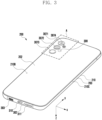
- FIG. 3 is a rear perspective view of the electronic device 200 according to an embodiment.
- a direction in which a display 301 included in the electronic device 200 is visually exposed is defined as a front surface, and a direction opposite thereto (e.g., -z-axis direction) is defined as a rear surface.
- the electronic device 200 may include a housing 210.
- the housing 210 may provide, for example, a front surface 210A of the electronic device 200, a rear surface 210B of the electronic device 200, and a lateral surface 210C of the electronic device 200.
- the housing 210 may refer to a structure including at least a part of the front surface 210A, the rear surface 210B, and the lateral surface 210C.
- the housing 210 may include a front plate (or first plate) 201, a rear plate (or second plate) 202, and a lateral member (or lateral bezel structure) 203.
- the electronic device 200 may include at least one of the display 301, a first audio module 302, a second audio module 303, a third audio module 304, a sensor module 305, a front camera module 306, a plurality of rear camera modules (e.g., a first rear camera module 3071, a second rear camera module 3072, a third rear camera module 3073, and a fourth rear camera module 3074), a light-emitting module 308, an input module 309, a first connection terminal module 310, and a second connection terminal module 311.
- the electronic device 200 may omit at least one of the above components or additionally include other components.
- the display 301 may include a pressure sensor capable of measuring the intensity (pressure) of a touch.
- the display 301 may be coupled to or positioned adjacent to a digitizer (e.g., an electromagnetic induction panel) configured to detect a magnetic field type electronic pen (e.g., a stylus pen).
- the display 301 may be implemented to include a digitizer.
- the second audio module 303 may include, for example, a first speaker positioned inside the electronic device 200, and a first speaker hole provided on the lateral surface 210C of the electronic device 200 to correspond to the first speaker.
- the third audio module 304 may include, for example, a second speaker positioned inside the electronic device 200, and a second speaker hole provided on the front surface 210A of the electronic device 200 to correspond to the second speaker.
- the second speaker may include a receiver for phone calls, and the second speaker hole may be referred to as a receiver hole.
- the position or number of the second audio module 303 or the third audio module 304 is not limited to the illustrated example and may vary.
- a microphone hole and a speaker hole may be implemented as one single hole.
- the second audio module 303 or the third audio module 304 may include a piezo speaker without a speaker hole.
- the optical sensor may be aligned and positioned in a recess provided on the rear surface of the display 301.
- the optical sensor may be disposed to overlap at least a part of a screen (or a display area) and perform its sensing function without being visually exposed.
- a partial area of the display 301 that at least partially overlaps the optical sensor may include a different pixel structure and/or wiring structure compared to other areas.
- a partial area of the display 301 that at least partially overlaps the optical sensor may have a different pixel density compared to other areas.
- a plurality of pixels may not be arranged in a partial area of the display 301 that at least partially overlaps the optical sensor.
- the electronic device 200 may include a biometric sensor (e.g., a fingerprint sensor) positioned on the rear surface of the display 301 or below or beneath the display 301.
- the biometric sensor may be implemented as an optical sensor, an electrostatic sensor, or an ultrasonic sensor, and the position or number thereof may vary.
- the electronic device 200 may further include at least one of various other sensor modules such as a gesture sensor, a gyro sensor, a barometric pressure sensor, a magnetic sensor, an acceleration sensor, a grip sensor, a color sensor, an infrared (IR) sensor, a temperature sensor, or a humidity sensor.
- a biometric sensor e.g., a fingerprint sensor
- the electronic device 200 may further include at least one of various other sensor modules such as a gesture sensor, a gyro sensor, a barometric pressure sensor, a magnetic sensor, an acceleration sensor, a grip sensor, a color sensor, an infrared (IR) sensor, a temperature sensor, or a humidity
- the front camera module 306 may be positioned inside the electronic device 200 to correspond to the front surface 210A of the electronic device 200.
- the plurality of rear camera modules 3071, 3072, 3073, and 3074 may be positioned inside the electronic device 200 to correspond to the rear surface 210B of the electronic device 200.
- the front camera module 306 and/or the rear camera module 3071, 3072, 3073, or 3074 may include one or more lenses, an image sensor, and/or an image signal processor.
- the position or number of camera modules is not limited to the illustrated example and may vary.
- the display 301 may include an opening aligned with the front camera module 306. External light may reach the front camera module 306 through the opening of the display 301 and the front plate 201.
- the opening of the display 301 aligned with or overlapping the front camera module 306 may be provided in the form of a notch.
- the opening of the display 301 aligned with or overlapping the front camera module 306 may be provided in the form of a hole.
- the front camera module 306 may be positioned on the rear surface of the display 301 or below or beneath the display 301, and the position of the front camera module 306 may perform a related function (e.g., image capturing) without the position of the front camera module 306 being visually distinguished (or exposed).
- the plurality of rear camera modules 3071, 3072, 3073, and 3074 may have different properties (e.g., an angle of view) or functions and may include, for example, a dual camera or a triple camera.
- the plurality of rear camera modules 3071, 3072, 3073, and 3074 may include a plurality of camera modules including lenses having different angles of view, and the electronic device 200 may be implemented to change an angle of view of a camera module performed by the electronic device 200, based on a user's selection.
- the plurality of rear camera modules 3071, 3072, 3073, and 3074 may include at least one of a wide-angle camera, a telephoto camera, a color camera, a monochrome camera, or an infrared (IR) camera (e.g., a time of flight (TOF) camera or a structured light camera).
- IR infrared
- TOF time of flight
- the IR camera may operate as at least a part of a sensor module.
- the rear plate 202 may include an opening corresponding to the light-emitting module 308 when viewed from above the rear plate 202.
- the light-emitting module 308 may be positioned through the opening of the rear plate 202.
- the rear plate 202 may be implemented to include substantially transparent light-transmitting areas, replacing the opening corresponding to the light-emitting module 308.
- the light-emitting module 308 may include a light source (e.g., a flash) for the plurality of rear camera modules 3071, 3072, 3073, and 3074.
- the light-emitting module 308 may include, for example, an LED or a xenon lamp.
- the second connection terminal module (e.g., a second connector module or a second interface terminal module) 311 may be used to mount an external storage medium (e.g., a SIM card or a memory card) to the electronic device 200.
- the second connection terminal module 311 may include, for example, a second connector (or a second interface terminal) positioned inside the electronic device 200, and a second connector hole provided on the lateral surface 210C of the electronic device 200 to correspond to the second connector.
- the second connection terminal module 311 may include a cover which is positioned (e.g., fitted into) in the second connector hole and forms a part of the lateral surface 210C of the electronic device 200.
- the second connection terminal module 311 may include a tray (or an adapter) (e.g., a SIM tray) for electrically or mechanically connecting an external storage medium to the second connector.
- the external storage medium may be disposed on the tray to be inserted into the second connector hole, and the external storage medium may be electrically connected to the second connector.
- the tray may be connected to a cover.
- the position or number of connection terminal modules is not limited to the illustrated example and may vary.
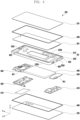
- FIG. 4 is an exploded perspective view of the electronic device 200 according to an embodiment.
- the electronic device 200 may include the front plate 201, the rear plate 202, the lateral member 203, a first support member 410, a second support member 420, a third support member 430, the display 301, a first board assembly 440, a second board assembly 450, a battery 460, an antenna structure 470, a first adhesive member 480, and/or a second adhesive member 490.
- the electronic device 200 may omit some of the above components or additionally include other components.
- the lateral member 203 may include a first lateral portion (or first bezel portion) 2031, a second lateral portion (or second bezel portion) 2032, a third lateral portion (or third bezel portion) 2033, and/or a fourth lateral portion (or fourth bezel portion) 2034.
- first lateral portion 2031 and the second lateral portion 2032 may be positioned to be spaced apart from each other in a first direction (e.g., y-axis direction) and may be substantially parallel to each other.
- the first lateral portion 2031 may provide a first lateral surface corresponding to the +y-axis direction of the electronic device 200 of the lateral surface 210C
- the second lateral portion 2032 may provide a second lateral surface corresponding to the -y-axis direction of the electronic device 200 of the lateral surface 210C.
- the third lateral portion 2033 may connect one end portion of the first lateral portion 2031 and one end portion of the second lateral portion 2032.
- the fourth lateral portion 2034 may connect the other end portion of the first lateral portion 2031 and the other end portion of the second lateral portion 2032.
- the third lateral portion 2033 and the fourth lateral portion 2034 may be positioned to be spaced apart from each other in a second direction (e.g., x-axis direction) perpendicular to the first direction and may be substantially parallel to each other.
- the third lateral portion 2033 may provide a third lateral surface corresponding to the +x-axis direction of the electronic device 200 of the lateral surface 210C
- the fourth lateral portion 2034 may provide a fourth lateral surface corresponding to the - x-axis direction of the electronic device 200 of the lateral surface 210C.
- a corner where the first lateral portion 2031 and the third lateral portion 2033 are connected, a corner where the first lateral portion 2031 and the fourth lateral portion 2034 are connected, a corner where the second lateral portion 2032 and the third lateral portion 2033 are connected, and/or a corner where the second lateral portion 2032 and the fourth lateral portion 2034 are connected may be implemented to have a smooth curved shape.
- the lateral member 203 may include a plurality of insulating portions 403 and a plurality of conductive portions separated from each other by the plurality of insulating portions 403.
- the lateral surface 210C (referring to FIG. 2 ) of the electronic device 200 may be provided by the plurality of conductive portions and the plurality of insulating portions 403.
- the lateral surface 210C may include first areas provided by the plurality of conductive portions included in the lateral member 203.
- the lateral surface 210C may include second areas provided by the plurality of insulating portions 403 included in the lateral member 203.
- the first areas and second areas of the lateral surface 210C may be smoothly connected without a substantial difference in height.
- the electronic components may include, for example, a microphone included in the first audio module 302, a first speaker included in the second audio module 303, a first connector included in the first connection terminal module 310, or a second connector included in the second connection terminal module 311.
- a processor e.g., the processor 120 of FIG. 1
- a wireless communication circuit e.g., the wireless communication module 192 of FIG. 1
- the processor may simultaneously perform position determination (AOA) which measures an angle, and position determination (ranging) which measures a distance.
- AOA angle of arrival
- ranging position determination
- the electronic device 200 may support a position determination function by using a broadband bandwidth (e.g., ultra-wide band (UWB)).
- a broadband bandwidth e.g., ultra-wide band (UWB)
- the UWB is a technology that follows the international standard of IEEE 802.15.4 and may refer to a technology which performs communication with a broadband bandwidth.
- the processor may identify or estimate a position of a signal source (e.g., a responder, a transmitter, or a Tx device) with respect to the electronic device 200 (e.g., an initiator, a receiver, or a receiver (Rx) device) by using a phase difference of signals received through a plurality of antenna elements included in the antenna structure 470.
- a signal source e.g., a responder, a transmitter, or a Tx device
- Rx receiver
- the second adhesive member 490 may be positioned between the rear plate 202 and the first support member 410, or between the rear plate 202 and the lateral member 203.
- the rear plate 202 may be coupled to the first support member 410 or the lateral member 203 by using the second adhesive member 490.
- the second adhesive member 490 may be disposed in an annular shape adjacent to the edge (or border) of the rear plate 202.
- the second adhesive member 490 may be disposed in various other forms which are not limited to the illustrated example.
- the second adhesive member 490 may include a plurality of adhesive members separated from each other. In this case, there may be a separate adhesive member or filling member which connects two adhesive members separated from each other.
- the first adhesive member 480 or the second adhesive member 490 may include a heat-reactive adhesive material, a photo-reactive adhesive material, a general adhesive, or a double-sided tape.
- the electronic device 100 or 200 may include an electronic device such as a bar type, a foldable type, a rollable type, a sliding type, a wearable type, a tablet PC, and/or a laptop PC.
- the electronic device 100 or 200 according to various embodiments of the disclosure is not limited to the examples described above and may include various other electronic devices.
- FIG. 5A is an exploded perspective view of a part of an electronic device 500 according to various embodiments.
- FIG. 5B is a cross-sectional view of the electronic device 500 according to various embodiments.
- FIG. 5A is an exploded perspective view of part A in FIG. 3 .
- FIG. 5B is a cross-sectional view taken along the B-B direction of FIG. 5A .
- the electronic device 500 may include a housing 510 (e.g., the housing 210 of FIGS. 2 to 4 ), at least one printed circuit board 502 (e.g., the first board assembly 440 and/or the second board assembly 450 of FIG. 4 ), an electrical component, and a flexible printed circuit board 530.
- the housing 510 may be a part which provides an internal space for arrangement of components of the electronic device 500 and protects the components of the electronic device 500.
- the housing 510 may include a frame 540 (e.g., the front case 40 of FIG. 4 ), a front plate 518 (e.g., the front plate 201 of FIGS.
- the electronic device 500 may include at least one antenna 508.
- the antenna 508 may be integrated with the housing 510 of the electronic device 500 to save or conserve the internal space of the electronic device 500 and improve the design of the electronic device 500.
- at least one of the plurality of metal segments 5411 of the lateral frame 541 may serve as the antenna 508.
- the metal segment 5411 serving as the antenna 508 may be electrically connected to the communication module.
- the flexible printed circuit board 530 may extend along one surface of an electrical component 520. In various embodiments, one surface of the electrical component 520 may face the support member 542, and the flexible printed circuit board 530 may extend between the one surface of the electrical component and the support member 542.
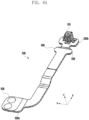
- FIG. 6A is a perspective view showing the flexible printed circuit board 530 according to various embodiments.
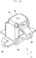
- FIG. 6B is a perspective view showing the contact member 531 according to various embodiments.
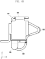
- FIG. 6D is a side view showing the contact member 531 according to various embodiments.
- a connector 539 may be disposed at first end portion 530a and the contact member 531 may be disposed at the second end portion 530b.
- the connector 539 may be a member configured to be connected to the printed circuit board 502 (and a wireless communication module disposed on the printed circuit board 502) of the electronic device 500.
- the connector 539 may be configured to be inserted and fixed into a socket disposed on the printed circuit board 502.
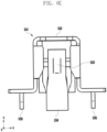
- the contact member 531 may be a member which forms electrical contact with the antenna 508 by applying an elastic force to a surface or portion of the antenna 508.
- a protrusion portion 538 formed by increasing a width (e.g., a dimension in the x-axis direction) of a section of the flexible printed circuit board 530 may be configured in an area adjacent to the second end portion 530b of the flexible printed circuit board 530. That is, a protrusion portion 538 may be provided in an area of the flexible printed circuit board 530 which is close to, near, or within a predetermined distance of the second end portion 530b of the flexible printed circuit board. The protrusion portion 538 may be provided in an area of the flexible printed circuit board which is at a predetermined distance from an end of the second end portion 530b.
- the protrusion portion 538 may be provided in an area of the flexible printed circuit board which is at a predetermined distance from the contact member 531.
- the protrusion portion 538 may be an area of the flexible printed circuit board which has a width greater than the width of a majority of the flexible printed circuit board 530.
- the protrusion portion 538 may be an area of the flexible printed circuit board with a width which is greater than a width of an adjacent area or region of the flexible printed circuit board 530.
- the protrusion portion 538 may have a width of at least 10%, 20%, 25%, 33% or 50% more than the width of an adjacent area of the flexible printed circuit board.
- the protrusion portion 538 may appear as a bulge in the width of the flexible printed circuit board.
- the extra width of the protrusion portion 538 may extend equally or substantially equally from either side of flexible printed circuit board such that the protrusion portion 538 is substantially symmetric with respect to an adjacent portion of the flexible printed circuit board 530.
- the width of the portions of the flexible printed circuit board 530 adjacent to and on either side of the protrusion portion 538 may be the same or substantially the same.
- the protrusion portion 538 may be a part which restricts the movement of the flexible printed circuit board 530 caused by the elastic force applied by the contact member 531. The action of the protrusion portion 538 will be described in more detail later.
- FIG. 7A is a plan view showing the frame 540 and the flexible printed circuit board 530 according to various embodiments of the disclosure.
- FIG. 7B is a cross-sectional view showing the frame 540 and the flexible printed circuit board 530 according to various embodiments of the disclosure.
- FIG. 7B is a cross-sectional view taken along the C-C direction of FIG. 7A .
- the support member 542 of the frame 540 may include a catching protrusion 543 configured at a part of the support member 542 corresponding to the protrusion portion 538 of the flexible printed circuit board 530.
- a surface of the support member 542 overlapping the protrusion portion 538 of the flexible printed circuit board 530 is recessed in the z direction, or a peripheral part of an area overlapping the protrusion portion 538 protrudes in the -z direction, so that the catching protrusion 543 may be formed.
- a reaction or reactive force is applied to the flexible printed circuit board 530, which may move the flexible printed circuit board 530 in a direction away from the antenna 508.
- This causes the contact member 531 on the flexible printed circuit board 530 to move away from the antenna 508, so the electric connection between the contact member 531 and the antenna 508 is weakened. Therefore, the elastic force applied by the contact member 531 to the antenna 508 to form electrical contact is weakened, and thus the electrical contact between the contact member 531 and the antenna 508 may become unstable or the contact resistance may increase. Therefore, the quality of a signal transmitted or received through the antenna 508 may deteriorate.
- the contact member 531 may form electrical contact with the antenna 508 by a sufficiently strong elastic force, and thus, the quality of a signal transmitted or received through the antenna 508 may be improved. That is, the catching protrusion 543 of the support member 542 catches or interacts with the protrusion portion 538 of the flexible printed circuit board 530 to prevent or reduce the movement of the flexible printed circuit board 530 away from the antenna 508 by the reactive force F. The contact member 531 therefore maintains a good contact with the antenna 508, so the quality of signal transmitted or received through the antenna 508 may be improved.
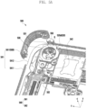
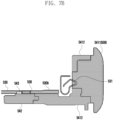
- FIG. 8A is a perspective view of the electronic device 500 according to various embodiments.
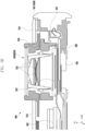
- FIG. 8B is a cross-sectional view of the electronic device 500 according to various embodiments.
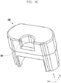
- FIG. 8C is a perspective view of the fixing member 550 according to various embodiments.
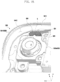
- FIG. 8E is a cross-sectional view of the electronic device 500 according to various embodiments.
- the cross section in FIG. 8B is a cross section taken in the D-D direction of FIG. 8A .
- the cross section in FIG. 8E is a cross section taken in the E-E direction of FIG. 8D .
- the electronic device 500 may include the fixing member 550.
- the fixing member 550 may be a member which restricts the flexible printed circuit board 530 from moving in a direction (e.g., -z direction) perpendicular to a surface of the flexible printed circuit board 530.
- the flexible printed circuit board 530 When the flexible printed circuit board 530 receives a reaction of an elastic force of the contact member 531 and the movement of the flexible printed circuit board 530 in the direction of the reaction is restricted (for example, by the protrusion portion 538), the flexible printed circuit board 530 may move in the direction perpendicular to the surface of the flexible printed circuit board 530 due to the reaction. For example, a force which bends the flexible printed circuit board 530 may be generated.
- the fixing member 550 may prevent or reduce the flexible printed circuit board 530 from being separated from its proper position by restricting such movement, and thus the electrical contact between the contact member 531 and the antenna 508 may be stably maintained.
- the electrical component 520 may include a flange 524 which fixes the fixing member 550 in the direction (e.g., -z direction) perpendicular to the surface of the flexible printed circuit board 530.
- the flange 524 may be disposed on the camera housing 521 of the camera 520a.
- the fixing member 550 may include a flange groove 551, and the flange 524 may be inserted into the flange groove 551.
- the flange groove 551 may be a groove formed to have a shape corresponding to the shape of the flange 524 on a surface in a direction (e.g., -z direction) in which the fixing member 550 comes into contact with the flange 524.
- the flange 524 is inserted into the flange groove 551, so that a separation of the fixing member 550 from a pressing force of the flange 524 may be prevented or reduced.
- the electronic device 500 may include an adhesive member 553 which bonds the fixing member 550 and the contact member 531 to each other.
- the adhesive member 553 may fix the fixing member 550 and the contact member 531 to each other to restrict the movement (e.g., tilt in the -z direction) of the contact member 531.
Landscapes
- Engineering & Computer Science (AREA)
- Microelectronics & Electronic Packaging (AREA)
- Computer Networks & Wireless Communication (AREA)
- Signal Processing (AREA)
- Telephone Set Structure (AREA)
Applications Claiming Priority (3)
| Application Number | Priority Date | Filing Date | Title |
|---|---|---|---|
| KR20230093981 | 2023-07-19 | ||
| KR1020230126520A KR20250015660A (ko) | 2023-07-19 | 2023-09-21 | 연성 회로 기판을 포함하는 전자 장치 |
| PCT/KR2024/010478 WO2025018844A1 (fr) | 2023-07-19 | 2024-07-19 | Dispositif électronique comprenant une carte de circuit imprimé souple |
Publications (2)
| Publication Number | Publication Date |
|---|---|
| EP4521858A1 true EP4521858A1 (fr) | 2025-03-12 |
| EP4521858A4 EP4521858A4 (fr) | 2025-09-10 |
Family
ID=93015058
Family Applications (1)
| Application Number | Title | Priority Date | Filing Date |
|---|---|---|---|
| EP24772196.2A Pending EP4521858A4 (fr) | 2023-07-19 | 2024-07-19 | Dispositif électronique comprenant une carte de circuit imprimé souple |
Country Status (3)
| Country | Link |
|---|---|
| EP (1) | EP4521858A4 (fr) |
| CN (1) | CN121533145A (fr) |
| WO (1) | WO2025018844A1 (fr) |
Family Cites Families (5)
| Publication number | Priority date | Publication date | Assignee | Title |
|---|---|---|---|---|
| US11258163B2 (en) * | 2018-08-30 | 2022-02-22 | Apple Inc. | Housing and antenna architecture for mobile device |
| KR102903457B1 (ko) * | 2020-11-30 | 2025-12-24 | 삼성전자주식회사 | 보강 부재를 포함하는 전자 장치 |
| KR102938422B1 (ko) * | 2021-03-19 | 2026-03-12 | 삼성전자주식회사 | 카메라 모듈을 포함하는 전자 장치 |
| KR20230007692A (ko) * | 2021-07-06 | 2023-01-13 | 삼성전자주식회사 | 안테나 및 그것을 포함하는 전자 장치 |
| KR20230076605A (ko) * | 2021-11-24 | 2023-05-31 | 삼성전자주식회사 | 메탈 안테나를 포함하는 전자 장치 |
-
2024
- 2024-07-19 CN CN202480047350.5A patent/CN121533145A/zh active Pending
- 2024-07-19 WO PCT/KR2024/010478 patent/WO2025018844A1/fr active Pending
- 2024-07-19 EP EP24772196.2A patent/EP4521858A4/fr active Pending
Also Published As
| Publication number | Publication date |
|---|---|
| WO2025018844A1 (fr) | 2025-01-23 |
| EP4521858A4 (fr) | 2025-09-10 |
| CN121533145A (zh) | 2026-02-13 |
Similar Documents
| Publication | Publication Date | Title |
|---|---|---|
| US11366532B2 (en) | Electronic device including antenna structure | |
| US12395578B2 (en) | Electronic device comprising housing | |
| US12519216B2 (en) | Electronic device including antenna and printed circuit board | |
| US12550280B2 (en) | Electronic device comprising antenna | |
| US20210057819A1 (en) | Antenna using multi feeding antenna and electronic device including same | |
| EP4239797A1 (fr) | Dispositif électronique comprenant une antenne à cadre | |
| US12295103B2 (en) | Electronic device including flexible printed circuit board | |
| US20240372936A1 (en) | Support structure and electronic device comprising same | |
| US12213242B2 (en) | Electronic device including a structure for guiding an arrangement position of an electronic component | |
| US20250274645A1 (en) | Electronic device including camera module | |
| US12230877B2 (en) | Antenna structure and electronic device with same | |
| US20250261352A1 (en) | Contact structure of camera module and electronic device comprising same | |
| US11563280B2 (en) | Electronic device including antenna | |
| US12341280B2 (en) | Electronic device including cable connector | |
| EP4521858A1 (fr) | Dispositif électronique comprenant une carte de circuit imprimé souple | |
| EP4546763B1 (fr) | Dispositif électronique comprenant un ensemble de touches | |
| EP4604317A1 (fr) | Dispositif électronique comprenant une structure conductrice pour améliorer les performances d'une antenne | |
| US20260101488A1 (en) | Electronic device including shielding structure for electronic component | |
| EP4426074A1 (fr) | Dispositif électronique comprenant une structure de masse pour carte de circuit imprimé souple | |
| EP4598293A1 (fr) | Dispositif électronique comprenant un boîtier de blindage | |
| KR20250015660A (ko) | 연성 회로 기판을 포함하는 전자 장치 | |
| US20250344321A1 (en) | Electronic device having structure for coupling module including electronic component to frame | |
| EP4492761A1 (fr) | Dispositif électronique comprenant une structure pour réduire l'entrée de substances étrangères | |
| US20250317506A1 (en) | Electronic device comprising structure for shielding printed circuit board including connector | |
| KR20250105562A (ko) | 안테나의 성능을 향상시키기 위한 도전성 구조를 포함하는 전자 장치 |
Legal Events
| Date | Code | Title | Description |
|---|---|---|---|
| STAA | Information on the status of an ep patent application or granted ep patent |
Free format text: STATUS: UNKNOWN |
|
| STAA | Information on the status of an ep patent application or granted ep patent |
Free format text: STATUS: THE INTERNATIONAL PUBLICATION HAS BEEN MADE |
|
| PUAI | Public reference made under article 153(3) epc to a published international application that has entered the european phase |
Free format text: ORIGINAL CODE: 0009012 |
|
| STAA | Information on the status of an ep patent application or granted ep patent |
Free format text: STATUS: REQUEST FOR EXAMINATION WAS MADE |
|
| 17P | Request for examination filed |
Effective date: 20240924 |
|
| AK | Designated contracting states |
Kind code of ref document: A1 Designated state(s): AL AT BE BG CH CY CZ DE DK EE ES FI FR GB GR HR HU IE IS IT LI LT LU LV MC ME MK MT NL NO PL PT RO RS SE SI SK SM TR |
|
| A4 | Supplementary search report drawn up and despatched |
Effective date: 20250811 |
|
| RIC1 | Information provided on ipc code assigned before grant |
Ipc: H05K 1/14 20060101AFI20250805BHEP Ipc: H01R 12/77 20110101ALI20250805BHEP Ipc: H01R 13/24 20060101ALI20250805BHEP Ipc: H01Q 1/24 20060101ALI20250805BHEP Ipc: H04M 1/02 20060101ALI20250805BHEP Ipc: H01B 7/08 20060101ALI20250805BHEP |
|
| GRAP | Despatch of communication of intention to grant a patent |
Free format text: ORIGINAL CODE: EPIDOSNIGR1 |
|
| STAA | Information on the status of an ep patent application or granted ep patent |
Free format text: STATUS: GRANT OF PATENT IS INTENDED |
|
| DAV | Request for validation of the european patent (deleted) | ||
| DAX | Request for extension of the european patent (deleted) | ||
| INTG | Intention to grant announced |
Effective date: 20260220 |