EP4521885A2 - Solarzellen für eine solarzellenanordnung - Google Patents
Solarzellen für eine solarzellenanordnung Download PDFInfo
- Publication number
- EP4521885A2 EP4521885A2 EP25153853.4A EP25153853A EP4521885A2 EP 4521885 A2 EP4521885 A2 EP 4521885A2 EP 25153853 A EP25153853 A EP 25153853A EP 4521885 A2 EP4521885 A2 EP 4521885A2
- Authority
- EP
- European Patent Office
- Prior art keywords
- solar cell
- conductors
- substrate
- solar cells
- solar
- Prior art date
- Legal status (The legal status is an assumption and is not a legal conclusion. Google has not performed a legal analysis and makes no representation as to the accuracy of the status listed.)
- Pending
Links
Images


Classifications
-
- H—ELECTRICITY
- H10—SEMICONDUCTOR DEVICES; ELECTRIC SOLID-STATE DEVICES NOT OTHERWISE PROVIDED FOR
- H10F—INORGANIC SEMICONDUCTOR DEVICES SENSITIVE TO INFRARED RADIATION, LIGHT, ELECTROMAGNETIC RADIATION OF SHORTER WAVELENGTH OR CORPUSCULAR RADIATION
- H10F19/00—Integrated devices, or assemblies of multiple devices, comprising at least one photovoltaic cell covered by group H10F10/00, e.g. photovoltaic modules
- H10F19/90—Structures for connecting between photovoltaic cells, e.g. interconnections or insulating spacers
- H10F19/902—Structures for connecting between photovoltaic cells, e.g. interconnections or insulating spacers for series or parallel connection of photovoltaic cells
- H10F19/904—Structures for connecting between photovoltaic cells, e.g. interconnections or insulating spacers for series or parallel connection of photovoltaic cells characterised by the shapes of the structures
-
- H—ELECTRICITY
- H10—SEMICONDUCTOR DEVICES; ELECTRIC SOLID-STATE DEVICES NOT OTHERWISE PROVIDED FOR
- H10F—INORGANIC SEMICONDUCTOR DEVICES SENSITIVE TO INFRARED RADIATION, LIGHT, ELECTROMAGNETIC RADIATION OF SHORTER WAVELENGTH OR CORPUSCULAR RADIATION
- H10F19/00—Integrated devices, or assemblies of multiple devices, comprising at least one photovoltaic cell covered by group H10F10/00, e.g. photovoltaic modules
- H10F19/70—Integrated devices, or assemblies of multiple devices, comprising at least one photovoltaic cell covered by group H10F10/00, e.g. photovoltaic modules comprising bypass diodes
-
- H—ELECTRICITY
- H10—SEMICONDUCTOR DEVICES; ELECTRIC SOLID-STATE DEVICES NOT OTHERWISE PROVIDED FOR
- H10F—INORGANIC SEMICONDUCTOR DEVICES SENSITIVE TO INFRARED RADIATION, LIGHT, ELECTROMAGNETIC RADIATION OF SHORTER WAVELENGTH OR CORPUSCULAR RADIATION
- H10F19/00—Integrated devices, or assemblies of multiple devices, comprising at least one photovoltaic cell covered by group H10F10/00, e.g. photovoltaic modules
- H10F19/80—Encapsulations or containers for integrated devices, or assemblies of multiple devices, having photovoltaic cells
-
- Y—GENERAL TAGGING OF NEW TECHNOLOGICAL DEVELOPMENTS; GENERAL TAGGING OF CROSS-SECTIONAL TECHNOLOGIES SPANNING OVER SEVERAL SECTIONS OF THE IPC; TECHNICAL SUBJECTS COVERED BY FORMER USPC CROSS-REFERENCE ART COLLECTIONS [XRACs] AND DIGESTS
- Y02—TECHNOLOGIES OR APPLICATIONS FOR MITIGATION OR ADAPTATION AGAINST CLIMATE CHANGE
- Y02E—REDUCTION OF GREENHOUSE GAS [GHG] EMISSIONS, RELATED TO ENERGY GENERATION, TRANSMISSION OR DISTRIBUTION
- Y02E10/00—Energy generation through renewable energy sources
- Y02E10/50—Photovoltaic [PV] energy
Definitions
- the disclosure is related generally to solar cell panels and, more specifically, to solar cells for a solar cell array.
- Typical spaceflight-capable solar cell panel assembly involves building long strings of solar cells. These strings are variable in length and can be very long, for example, up to and greater than 20 cells. Assembling such long, variable, and fragile materials is difficult, which has prevented automation of the assembly.
- CIC cell, interconnect and coverglass
- the CIC has metal foil interconnects connected to the front of the cell that extend in parallel from one side of the CIC.
- the CICs are located close to each other and the interconnects make connection to the bottom of an adjacent cell.
- the CICs are assembled into linear strings. These linear strings are built-up manually and then laid out to form a large solar cell array comprised of many strings of variable length.
- bypass diode is used to protect the cells from reverse bias, when the cells become partially shadowed.
- the bypass diode generally connects the back contacts of two adjacent cells within the solar cell array.
- the solar cell array When used in a satellite, the solar cell array is typically packaged as a panel.
- the dimensions of the panel are dictated by the needs of the satellite, including such constraints as needed power, as well as the size and shape necessary to pack and store the satellite in a launch vehicle. Furthermore, the deployment of the panel often requires that some portions of the panel are used for the mechanical fixtures and the solar cell array must avoid these locations. In practice, the panel is generally rectangular, but its dimensions and aspect ratio vary greatly. The layout of the CICs and strings to fill this space must be highly customized for maximum power generation, which results in a fabrication process that is highly manual.
- a new approach to the design of solar cell arrays is based on electrical connections among the solar cells in the array.
- This new approach rearranges the components of a solar cell and the arrangements of the solar cells in the array. Instead of having solar cells connected into long linear strings and then assembled onto a substrate, the solar cells are attached individually to a substrate, such that corner regions of adjacent cells are aligned on the substrate, thereby exposing an area of the substrate. Electrical connections between cells are made by corner conductors formed on or in the substrate in these corner regions. Consequently, this approach presents a solar cell array design based on individual cells.
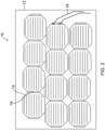
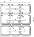
- FIGS. 1 and 2 illustrate conventional structures for solar cell panels 10, which include a substrate 12, a plurality of solar cells 14 arranged in an array, and electrical connectors 16 between the solar cells 14.
- Half size solar cells 14 are shown in FIG. 1 and full size solar cells 14 are shown in FIG. 2 .
- Space solar cells 14 are derived from a round Germanium (Ge) substrate starting material, which is later fabricated into semi-rectangular shapes to improve dense packing onto the solar cell panel 10. This wafer is often diced into one or two solar cells 14 herein described as half size or full size solar cells 14.
- the electrical connectors 16 providing electrical connections between solar cells 14 are made along the long parallel edge between solar cells 14. These series connections (cell-to-cell) are completed off-substrate, as strings of connected solar cells 14 are built having lengths of any number of solar cells 14. The completed strings of solar cells 14 are then applied and attached to the substrate 12.
- wiring 18 is attached at the end of a string of solar cells 14 to electrically connect the string to other strings, or to terminate the resulting circuit and bring the current off of the array of solar cells 14.
- String-to-string and circuit termination connections are typically done on the substrate 12, and typically using wiring 18.
- some small solar cell panels 10 use a printed circuit board (PCB)-type material with embedded conductors.
- PCB printed circuit board
- Adjacent strings of connected solar cells 14 can run parallel or anti-parallel.
- strings of connected solar cells 14 can be aligned or misaligned. There are many competing influences to the solar cell 14 layout resulting in regions where solar cells 14 are parallel or anti-parallel, aligned or misaligned.
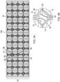
- FIGS. 3A-3B illustrate improved devices and structures for a solar cell panel 10a, according to one example, wherein FIG. 3B is an enlarged view of the details in the dashed circle in FIG. 3A .
- the various components of the solar cell panel 10a are shown and described in greater detail in FIGS. 5-14 .
- the solar cell panel 10a includes a substrate 12 for solar cells 14 having one or more corner conductors 20 thereon.
- the substrate 12 is a multi-layer substrate 12 comprised of one or more Kapton ® (polyimide) layers separating one or more patterned metal layers.
- Kapton ® polyimide
- the substrate 12 may be mounted on a large rigid panel 10a similar to conventional assembles. Alternatively, substrate 12 can be mounted to a lighter more sparse frame or panel 10a for mounting or deployment.
- a plurality of solar cells 14 are attached to the substrate 12 in a two-dimensional (2D) grid of an array 22.
- the array 22 is comprised of ninety-six (96) solar cells 14 arranged in four (4) rows by twenty-four (24) columns, but it is recognized that any number of solar cells 14 may be used in different implementations.
- the array 22 could be comprised of forty-eight (48) full-size solar cells 14 arranged in four (4) rows by twelve (12) columns, wherein each of the full-size solar cells 14 is configured in a manner similar to two half-size solar cells 14 arranged back-to-back (see, e.g., FIGS. 16-24 below).
- At least one of the solar cells 14 has at least one cropped corner 24 that defines a corner region 26, as indicated by the dashed circle.
- the solar cells 14 are attached to the substrate 12, such that corner regions 26 of adjacent ones of the solar cells 14 are aligned, thereby exposing an area 28 of the substrate 12.
- the area 28 of the substrate 12 that is exposed includes one or more of the corner conductors 20, and one or more electrical connections between the solar cells 14 and the corner conductors 20 are made in the corner regions 26 resulting from the cropped corners 24 of the solar cells 14.
- the corner conductors 20 are conductive paths attached to, printed on, buried in, or deposited on the substrate 12, before and/or after the solar cells 14 are attached to the substrate 12, which facilitate connections between adjacent solar cells 14.
- the connections between the solar cells 14 and the corner conductors 20 are made after the solar cells 14 have been attached to the substrate 12.
- four adjacent solar cells 14 are aligned on the substrate 12, such that four cropped corners 24, one from each solar cell 14, are brought together at the corner regions 26.
- the solar cells 14 are then individually attached to the substrate 12, wherein the solar cells 14 are placed on top of the corner conductors 20 to make the electrical connection between the solar cells 14 and the corner conductors 20.
- the solar cells 14 may be applied to the substrate 12 as CIC (cell, interconnect and coverglass) units.
- CIC cell, interconnect and coverglass
- a bare solar cell 14 may be applied to the substrate 12, and the coverglass later applied to the front of the solar cell 14 with a transparent adhesive. This assembly protects the solar cells 14 from damage from space radiation that would limit performance.
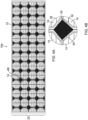
- FIGS. 4A and 4B illustrate an alternative structure for the solar cell panel 10a, according to one example, wherein FIG. 4B is an enlarged view of the details in the dashed circle in FIG. 4A .
- FIG. 4B is an enlarged view of the details in the dashed circle in FIG. 4A .
- PRM power routing module
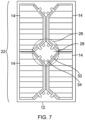
- FIG. 5 illustrates the front side of an exemplary solar cell 14 that may be used in the improved solar cell panel 10a of FIGS. 3A-3B and 4A-4B .
- the solar cell 14, which is a CIC unit, is a half-size solar cell 14. (Full-size solar cells 14 could also be used.)
- the solar cell 14 is fabricated having at least one cropped corner 24 that defines a corner region 26, as indicated by the dashed circle, such that the corner region 26 resulting from the cropped corner 24 includes at least one contact 32, 34 for making an electrical connection to the solar cell 14.
- the solar cell 14 has two cropped corners 24, each of which has both a front contact 32 on the front side of the solar cell 14 and a back contact 34 on a back side of the solar cell 14, where the contacts 32 and 34 extend into the corner region 26.
- Full-size solar cells 14 would have four cropped corners 24, each of which would have a front contact 32 and a back contact 34.
- the cropped corners 24 increase utilization of the round wafer starting materials for the solar cells 14. In conventional panels 10, these cropped corners 24 would result in unused space on the panel 10 after the solar cells 14 are attached to the substrate 12.
- the new approach described in this disclosure utilizes this unused space. Specifically, metal foil interconnects, comprising the corner conductors 20, front contacts 32 and back contacts 34, are moved to the corner regions 26.
- existing CICs have interconnects attached to the solar cell 14 front side, and connect to the back side (where connections occur) during stringing.
- the current generated by the solar cell 14 is collected on the front side of the solar cell 14 by one or more grids 36 comprised of thin metal fingers 38 and wide bus bars 40 that are connected to both of the front contacts 32.
- the bus bar 40 is a low resistance conductor that carries high currents and also provides redundancy should a front contact 32 become disconnected. Optimization generally desires a short bus bar 40 running directly between the front contacts 32. Having the front contact 32 in the cropped corner 24 results in moving the bus bar 40 away from the perimeter of the solar cell 14. This is achieved while simultaneously minimizing the bus bar 40 length and light obscuration.
- the fingers 38 are now shorter. This reduces parasitic resistances in the grid 36, because the length of the fingers 38 is shorter and the total current carried is less. This produces a design preference where the front contacts 32 and connecting bus bar 40 is moved to provide shorter narrow fingers 38.
- FIG. 6 illustrates the back side of the exemplary solar cell 14 of FIG. 5 .
- the back side of the solar cell 14 is covered by a full area metal back layer 42 that is connected to both of the back contacts 34.
- FIG. 7 illustrates solar cells 14 arranged into the 2D grid of the array 22, according to one example.
- the array 22 comprises a plurality of solar cells 14 attached to a substrate 12, such that corner regions 26 of adjacent ones of the solar cells 14 are aligned, thereby exposing an area 28 of the substrate 12. Electrical connections (not shown) between the solar cells 14 are made in the exposed area 28 of the substrate 12 using the front contacts 32 and back contacts 34 of the solar cells 14 and corner conductors 20 (not shown) formed on or in the exposed area 28 of the substrate 12.
- the solar cells 14 are individually attached to the substrate 12. This assembly can be done directly on a support surface, i.e., the substrate 12, which can be either rigid or flexible. Alternatively, the solar cells 14 could be assembled into the 2D grid of the array 22 on a temporary support surface and then transferred to a final support surface, i.e., the substrate 12.
- FIG. 8 illustrates an example of the array 22 where one or more bypass diodes 44 are added to the exposed area 28 of the substrate 12 in the corner regions 26, for use in one or more of the electrical connections.
- the bypass diodes 44 protect the solar cells 14 when the solar cells 14 become unable to generate current, which could be due to being partially shadowed, which drives the solar cells 14 into reverse bias.
- the bypass diodes 44 are attached to the substrate 12 in the corner regions 26 independent of the solar cells 14.
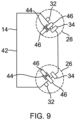
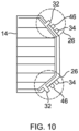
- FIG. 9 illustrates an example where the bypass diode 44 is applied to the back side of the solar cell 14, with an interconnect or contact 46 for the bypass diode 44 extending into the corner region 26 between the front and back contacts 32, 34.
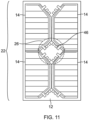
- FIG. 11 illustrates the solar cells 14 of FIGS. 9 and 10 arranged into the 2D grid of the array 22 and applied to the substrate 12, where the bypass diodes 44 (not shown) are applied to the back side of the solar cells 14, with the contacts 46 for the bypass diodes 44 extending into the corner regions 26 of the solar cells 14.
- FIGS. 7 , 8 and 11 are generalized layouts. Specifically, these layouts can be repeated across any panel 10a dimensions desired by a customer. This greatly simplifies assembly, rework, test, and inspection processes.
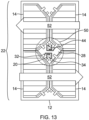
- the electrical connections are series connections that determine a flow of current through the plurality of solar cells 14. This may be accomplished by the connection schemes shown in FIGS. 12 and 13 , wherein FIG. 12 shows up/down series connections 48 between the solar cells 14 of the array 22, and FIG. 13 shows left/right series connections 50 between the solar cells 14 of the array 22.
- these series connections 48, 50 are electrical connections between the front contacts 32 and back contacts 34 of the solar cells 14, and the bypass diodes 44, are made using the corner conductors 20 formed on or in the exposed areas 28 of the substrate 12.
- These series connections 48, 50 determine the current (power) flow, as indicated by the arrows 52, through the solar cells 14, in contrast to the assembly of large strings off-substrate.
- FIG. 14 shows a side view of an example wherein the substrate 12 is a flex sheet assembly including multilayer conductors.
- the substrate 12 includes a polyimide base layer 54 with Cu layer 56a above and Cu layer 56b below, wherein Cu layers 56a, 56b may be patterned as the corner conductors 20, other conductors, power lines, common lines, bridging lines, etc. Note that there may be one or multiple Cu layers 56a, 56b with polyimide layers 54 positioned between each of the layers 56a, 56b.
- a conducting back sheet of polyimide 58 can be applied to the polyimide layer 54, which is useful in a space environment in that it will reduce the accumulation of charge.
- Another capability is the addition of a plated Silver (Ag) or Gold (Au) layer 60 on the Cu layer 56a as part of the corner conductors 20, which improves the ability to make connections.
- the solar cell 14 Shown on the right side is the solar cell 14 that is attached to the substrate 12 with adhesive 62. Also visible is the metal foil interconnect 64 attached to the solar cell 14 and the plated Ag or Au layer 60 of the corner conductors 20.
- this new approach attaches the solar cells 14 individually to a substrate 12 such that the corner regions 26 of two, three or four adjacent solar cells 14 are aligned on the substrate 12.
- the solar cells 14 are laid out so that the cropped corners 24 are aligned and the corner regions 26 are adjacent, thereby exposing an area 28 of the substrate 12.
- Electrical connections between solar cells 14 are made in these corner regions 26 between front contacts 32 and back contacts 34 on the solar cells 14, bypass diodes 44, and corner conductors 20 on or in the exposed area 28 of the substrate 12, wherein these conductive paths are used to create a string of solar cells 14 in a series connection 48, 50 comprising a circuit.
- the result is that more electrical connections are available in more corners, which simplifies the corner connections and provides redundancy.
- FIG. 15B shows a wafer 70 with a pair of rectangular half-size solar cells 14, where there is a large area around the perimeters of the solar cells 14 that will be discarded. This discarded area is highly valuable, and it is desirable to maximize the utilization of the wafer material.
- FIG. 15C shows a wafer 70 with a pair of half-size solar cells 14 having cropped corners 24, wherein the cropped corners 24 improve utilization of the wafer 70 area. Specifically, there is a smaller area around the perimeters of the solar cells 14 that will be discarded, as compared to FIG. 15B .
- FIG. 15D shows a wafer 70 with a single full-size solar cell 14 having cropped corners 24.
- the cropped corners 24 of the single full-size solar cell 14 improve utilization of the wafer 70 area. Specifically, there is a smaller area around the perimeters of the solar cells 14 that will be discarded, as compared to FIG. 15B , wherein the area is roughly equivalent to the area around the perimeters of the solar cells 14 that will be discarded in FIG. 15C .
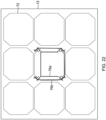
- FIG. 16 shows a structure where nine (9) full-size solar cells 14 are assembled together in a solar cell array 22 comprised of three (3) rows by three (3) columns.
- Multiple grids 36 are shown in the face of the center solar cell 14, wherein each of the grids 36 terminate at one or more of the front contacts 32 of the solar cell 14. (Similar grids 36 would be present on the other solar cells 14 in the array 22, but are omitted to simplify the figure.)
- the length of the fingers 38 in each of the grids 36 can be minimized, as compared to a conventional structure for extracting current from a single side of the solar cell 14.
- These four terminations minimize the distance the current needs to flow, which reduces the impact of resistance.
- each termination carries one-fourth of the solar cell's current, thereby reducing energy loss, which is determined by the current squared.
- FIG. 17 illustrates the use of buried conductors, according to one example.
- the solar cells 14 are omitted from this view, with their positions 72 when mounted on the substrate 12 indicated by dashed outlines.
- the substrate 12 includes conductors 74a, 74b under or alongside each of the cell positions 72.
- the conductors 74a, 74b are buried conductors patterned in one or more of the Cu layers 56a, 56b of the substrate 12.
- An insulation layer is placed between these conductors 74a, 74b and the solar cells 14.
- the conductors 74a, 74b are both patterned in the same Cu layer 56a, 56b.
- the conductors 74a, 74b can also be patterned in different Cu layers 56a, 56b.
- the conductors 74a, 74b are loops.
- different shapes may be used, as described in FIGS. 22 , 23 , and 24 below.
- the conductor 74a connects to the front contacts 32 of the solar cell 14 and the conductor 74b connects to the back contacts 34 of the solar cell 14 (which are shown without the solar cell 14 present). This configuration may be reversed, with the conducting loop of the back contact 34 being inside the conducting loop of the front contact 32
- the conductors 74a, 74b are completely covered by the top polyimide overlay layer 66a, and are connected to the front contacts 32 and back contacts 34 of the solar cell 14 using the vias 68 between layers in the substrate 12. Portions of the conductors 74a, 74b can be exposed through the top polyimide overlay layer 66a, and are connected to the front contacts 32 and back contacts 34 of the solar cell 14 by interconnects.
- the conductor 74a can connect to one or more of the four front contacts 32 on the solar cell 14 and the conductor 74b can connect to one or more of the four back contacts 34 on the solar cell 14. This provides redundancy, in case there is a failure of an interconnect or conducting trace.
- the conductors 74a, 74b do not block any light from entering the solar cells 14. In addition, due to their shape, the conductors 74a, 74b carry current to all sides and corners of the solar cell 14. Preferably, the conductors 74a, 74b are comprised of sufficient metal to be low resistance paths.
- FIG. 18 illustrates one example of series connections between conductors 74a, 74b for adjacent solar cell positions 72 of the substrate 12. Again, the solar cells 14 are omitted from this view, with their positions 72 on the substrate 12 indicated by dashed outlines. Only the connections adjacent to the center solar cell 14 are fully drawn.
- the arrows 52 show the overall direction of current (power) between the cell positions 72.
- the solar cell's 14 current flows from the front of the solar cell 14 to the backside of the solar cell 14, and then continues to the next solar cell 14 in the string.
- the series connections are made in the corner regions 26 surrounding the center cell position 72, and include corner conductors 20 and bypass diodes 44.
- the series connections and bypass diodes 44 are similar to the example in FIG. 12 , wherein each full size solar cell 14 has a series connection and a bypass diode 44 on both sides leading to the next solar cell 14 in series.
- FIG. 19 illustrates another example of series connections between conductors 74a, 74b for adjacent solar cell positions 72 of the substrate 12. Again, the solar cells 14 are omitted from this view, with their positions 72 on the substrate 12 indicated by dashed outlines. Only the connections adjacent to the center solar cell 14 are fully drawn.
- the arrows 52 show the overall direction of current (power) between the cell positions 72.
- the series connections are again made in the corner regions 26 surrounding the center cell position 72, and include corner conductors 20 and bypass diodes 44.
- each cell position 72 in the first and second columns has only one series connection that includes the corner conductors 20 and one bypass diode 44, leaving the third column open.
- there are fewer corner conductors 20 in the series connections which can result in less space used on the substrate 12 and higher output, or more widely spaced conductors with a greater resistance to electrostatic discharge (ESD) that operate at higher voltage levels.
- ESD electrostatic discharge
- FIG. 20 illustrates another example of series connections between conductors 74a, 74b for adjacent cell positions 72 of the substrate 12. Again, the solar cells 14 are omitted from this view, with their positions 72 on the substrate 12 indicated by dashed outlines. Only the connections adjacent to the center solar cell 14 are fully drawn.
- the arrows 52 show the overall direction of current (power) between the cell positions 72.
- the series connections are made only in a subset of the corner regions 26 surrounding the center cell position 72, and include corner conductors 20 and bypass diodes 44.
- the series connections and bypass diodes 44 are only made on one side of the solar cells 14.
- the series connections and bypass diodes 44 for the first and second columns of solar cells 14 are made in the space between these solar cells 14. Between the second and third rows of solar cells 14, there are no series connections or bypass diodes 44.
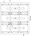
- FIG. 21 illustrates another example of series connections between conductors 74a, 74b for adjacent cell positions 72 of the substrate 12. Again, the solar cells 14 are omitted from this view, with their positions 72 on the substrate 12 indicated by dashed outlines.
- the arrows 52 show the overall direction of current (power) between the cell positions 72.
- the series connections are again made in the corner regions 26 surrounding the center cell position 72, and include corner conductors 20 and bypass diodes 44. Only the connections adjacent to the center solar cell 14 are fully drawn.
- the series connections are made on both sides of the solar cell 14 adjacent to the next solar cell 14 in series.
- the bypass diode 44 is only located on one side.
- FIG. 22 illustrates a variation in the configuration of buried conductors in the substrate 12.
- each of the conductors 76a, 76b is U-shaped, with two substantially linear portions connected by an arcuate portion, where the linear portions are substantially parallel to each other.
- Each of the conductors 76a, 76b connect to all four cropped corners 24 around the perimeter of the cell position 72.
- FIG. 23 also illustrates a variation in the configuration of buried conductors in the substrate 12.
- the conductors 78a, 78b have only up or down pathways that connect the cropped corners 24 of the cell position 72 in the up/down direction of the current flow 52. This allows the conductors 78a, 78b to pass inside or outside of each other, without crossing.
- the conductors 78a, 78b can be patterned in a single Cu layer 56a or Cu layer 56b without need for vias 68, which simplifies fabrication of the circuit.
- this configuration does require series connection on both sides of the cell position 72.
- the back layer 42 of the solar cell 14 enables a single bypass diode 44 to be used.
- FIG. 24 illustrates another variation in the buried conductors in the substrate 12.
- the back contact 34 does not connect to a buried conductor. Instead, the back layer 42 of the solar cell 14 is used to carry current to the back contacts 34 of the solar cell 14, which eliminates the need for a buried conductor.
- the back contacts 34 carry current to the series-connected adjacent cell positions 72 via corner conductors 20. There is also a bypass diode 44 in these series connections.
- the conductor 80 connects between two front contacts 32 parallel to the direction of current flow 52, which in this example is up/down and not left/right.
- Examples of the disclosure may be described in the context of a method 82 of fabricating a solar cell 14, solar cell panel 10a and/or satellite, comprising steps 84-96, as shown in FIG. 25 , wherein the resulting satellite 98 having a solar cell panel 10a comprised of solar cells 14 are shown in FIG. 26 .
- exemplary method 82 may include specification and design 84 of the solar cell 14, solar cell panel 10a and/or satellite 98, and material procurement 86 for same.
- component and subassembly manufacturing 88 and system integration 90 of the solar cell 14, solar cell panel 10a and/or satellite 98 takes place, which include fabricating the solar cell 14, solar cell panel 10a and/or satellite 98.
- the solar cell 14, solar cell panel 10a and/or satellite 98 may go through certification and delivery 92 in order to be placed in service 94.
- the solar cell 14, solar cell panel 10a and/or satellite 98 may also be scheduled for maintenance and service 96 (which includes modification, reconfiguration, refurbishment, and so on), before being launched.
- a system integrator may include without limitation any number of solar cell, solar cell panel, satellite or spacecraft manufacturers and major-system subcontractors;
- a third party may include without limitation any number of venders, subcontractors, and suppliers; and
- an operator may be a satellite company, military entity, service organization, and so on.
- a satellite 98 fabricated by exemplary method 82 may include systems 100, a body 102, solar cell panels 10a comprised of solar cells 14, and one or more antennae 104.
- the systems 100 included with the satellite 98 include, but are not limited to, one or more of a propulsion system 106, an electrical system 108, a communications system 110, and a power system 112. Any number of other systems 100 also may be included.
- FIG. 27 is an illustration of the solar cell panel 10a in the form of a functional block diagram, according to one example.
- the solar cell panel 10a is comprised of the solar cell array 22, which is comprised of one or more of the solar cells 14 individually attached to the substrate 12.
- Each of the solar cells 14 absorbs light 114 from a light source 116 and generates an electrical output 118 in response thereto.
- At least one of the solar cells 14 has at least one cropped corner 24 that defines a corner region 26, such that an area 28 of the substrate 12 remains exposed when the solar cell 14 is attached to the substrate 12.
- the corner regions 26 of adjacent ones of the solar cells 14 are aligned, thereby exposing the area 28 of the substrate 12.
- the area 28 of the substrate 12 that remains exposed includes one or more corner conductors 20 attached to, printed on, or integrated with the substrate 12, and one or more electrical connections between the solar cells 14 and the corner conductors 20 are made in a corner region 26.
- the corner region 26 may also include one or more bypass diodes 44.
- the corner region 26 includes at least one contact, for example, a front contact 32 on a front side of the solar cell 14 and/or a back contact 34 on a back side of the solar cell 14.
- the substrate 12 may include buried conductors 74a, 74b, 76a, 76b, 78a, 78b, 80, wherein the buried conductors 74a, 74b, 76a, 76b, 78a, 78b, 80 provide conductive paths for the front and back contacts 32, 34 of the solar cell 14.
- the buried conductors 74a, 74b, 76a, 76b, 78a, 78b, 80 also facilitate connections between solar cells 14.
Landscapes
- Photovoltaic Devices (AREA)
Applications Claiming Priority (20)
| Application Number | Priority Date | Filing Date | Title |
|---|---|---|---|
| US201662394632P | 2016-09-14 | 2016-09-14 | |
| US201662394636P | 2016-09-14 | 2016-09-14 | |
| US201662394629P | 2016-09-14 | 2016-09-14 | |
| US201662394616P | 2016-09-14 | 2016-09-14 | |
| US201662394666P | 2016-09-14 | 2016-09-14 | |
| US201662394623P | 2016-09-14 | 2016-09-14 | |
| US201662394641P | 2016-09-14 | 2016-09-14 | |
| US201662394649P | 2016-09-14 | 2016-09-14 | |
| US201662394667P | 2016-09-14 | 2016-09-14 | |
| US201662394672P | 2016-09-14 | 2016-09-14 | |
| US201662394671P | 2016-09-14 | 2016-09-14 | |
| US201662394627P | 2016-09-14 | 2016-09-14 | |
| US201515643287A | 2017-07-06 | 2017-07-06 | |
| US15/643,277 US12615851B2 (en) | 2016-09-14 | 2017-07-06 | Prefabricated conductors on a substrate to facilitate corner connections for a solar cell array |
| US15/643,285 US20180076761A1 (en) | 2016-09-14 | 2017-07-06 | Power routing module with a switching matrix for a solar cell array |
| US15/643,274 US20180076346A1 (en) | 2016-09-14 | 2017-07-06 | Solar cell array connections using corner conductors |
| US15/643,279 US20180076348A1 (en) | 2016-09-14 | 2017-07-06 | Rework and repair of components in a solar cell array |
| US15/643,289 US11437533B2 (en) | 2016-09-14 | 2017-07-06 | Solar cells for a solar cell array |
| US15/643,282 US20180076349A1 (en) | 2016-09-14 | 2017-07-06 | Power routing module for a solar cell array |
| EP17191175.3A EP3297040B1 (de) | 2016-09-14 | 2017-09-14 | Solarzellen für solarzellenanordnung |
Related Parent Applications (2)
| Application Number | Title | Priority Date | Filing Date |
|---|---|---|---|
| EP17191175.3A Division-Into EP3297040B1 (de) | 2016-09-14 | 2017-09-14 | Solarzellen für solarzellenanordnung |
| EP17191175.3A Division EP3297040B1 (de) | 2016-09-14 | 2017-09-14 | Solarzellen für solarzellenanordnung |
Publications (2)
| Publication Number | Publication Date |
|---|---|
| EP4521885A2 true EP4521885A2 (de) | 2025-03-12 |
| EP4521885A3 EP4521885A3 (de) | 2025-05-21 |
Family
ID=94600852
Family Applications (1)
| Application Number | Title | Priority Date | Filing Date |
|---|---|---|---|
| EP25153853.4A Pending EP4521885A3 (de) | 2016-09-14 | 2017-09-14 | Solarzellen für eine solarzellenanordnung |
Country Status (1)
| Country | Link |
|---|---|
| EP (1) | EP4521885A3 (de) |
Family Cites Families (8)
| Publication number | Priority date | Publication date | Assignee | Title |
|---|---|---|---|---|
| US5567248A (en) * | 1995-09-05 | 1996-10-22 | Chung; Darius | Modular solar cell contact arrangement |
| DE10136442A1 (de) * | 2001-07-26 | 2003-02-13 | Ralf Adelhelm | Kontakte und Verbinder von Solarzellen |
| FR2864347B1 (fr) * | 2003-12-23 | 2006-03-03 | Cit Alcatel | Panneau generateur solaire et satellite associe |
| JP2012186314A (ja) * | 2011-03-04 | 2012-09-27 | Sharp Corp | 太陽電池モジュール |
| DE102012003455A1 (de) * | 2012-02-22 | 2013-08-22 | Mühlbauer Ag | Verfahren und Vorrichtung zur Herstellung eines Solarmoduls und ein Solarmodul mit flexiblen Dünnschicht-Solarzellen |
| US9627565B2 (en) * | 2013-11-27 | 2017-04-18 | Space Systems/Loral, Llc | Integral corner bypass diode interconnecting configuration for multiple solar cells |
| JP6422426B2 (ja) * | 2014-12-09 | 2018-11-14 | 三菱電機株式会社 | 太陽電池 |
| US20160218665A1 (en) * | 2015-01-22 | 2016-07-28 | Solaero Technologies Corp. | Space solar cell panel with blocking diodes |
-
2017
- 2017-09-14 EP EP25153853.4A patent/EP4521885A3/de active Pending
Also Published As
| Publication number | Publication date |
|---|---|
| EP4521885A3 (de) | 2025-05-21 |
Similar Documents
| Publication | Publication Date | Title |
|---|---|---|
| JP7607014B2 (ja) | ソーラーセルアレイ用のソーラーセル | |
| US12100774B2 (en) | Solar cells for a solar cell array | |
| EP3297035B1 (de) | Solarzellenanordnungsverbindungen mit verwendung von eckleitern | |
| EP3416198B1 (de) | Solarzellenanordnung mit veränderbarer stranglänge | |
| EP4521885A2 (de) | Solarzellen für eine solarzellenanordnung | |
| EP3297040A1 (de) | Solarzellen für solarzellenanordnung |
Legal Events
| Date | Code | Title | Description |
|---|---|---|---|
| PUAI | Public reference made under article 153(3) epc to a published international application that has entered the european phase |
Free format text: ORIGINAL CODE: 0009012 |
|
| STAA | Information on the status of an ep patent application or granted ep patent |
Free format text: STATUS: THE APPLICATION HAS BEEN PUBLISHED |
|
| AC | Divisional application: reference to earlier application |
Ref document number: 3297040 Country of ref document: EP Kind code of ref document: P |
|
| AK | Designated contracting states |
Kind code of ref document: A2 Designated state(s): AL AT BE BG CH CY CZ DE DK EE ES FI FR GB GR HR HU IE IS IT LI LT LU LV MC MK MT NL NO PL PT RO RS SE SI SK SM TR |
|
| REG | Reference to a national code |
Ref country code: DE Ref legal event code: R079 Free format text: PREVIOUS MAIN CLASS: H10F0019700000 Ipc: H10F0019900000 |
|
| PUAL | Search report despatched |
Free format text: ORIGINAL CODE: 0009013 |
|
| AK | Designated contracting states |
Kind code of ref document: A3 Designated state(s): AL AT BE BG CH CY CZ DE DK EE ES FI FR GB GR HR HU IE IS IT LI LT LU LV MC MK MT NL NO PL PT RO RS SE SI SK SM TR |
|
| RIC1 | Information provided on ipc code assigned before grant |
Ipc: H10F 10/142 20250101ALI20250414BHEP Ipc: H10F 19/80 20250101ALI20250414BHEP Ipc: H10F 19/70 20250101ALI20250414BHEP Ipc: H10F 77/14 20250101ALI20250414BHEP Ipc: H10F 77/00 20250101ALI20250414BHEP Ipc: H10F 19/90 20250101AFI20250414BHEP |
|
| STAA | Information on the status of an ep patent application or granted ep patent |
Free format text: STATUS: REQUEST FOR EXAMINATION WAS MADE |
|
| 17P | Request for examination filed |
Effective date: 20250924 |