EP4524104A1 - Sphärische einkristall-siliciumnanopartikel - Google Patents
Sphärische einkristall-siliciumnanopartikel Download PDFInfo
- Publication number
- EP4524104A1 EP4524104A1 EP22941696.1A EP22941696A EP4524104A1 EP 4524104 A1 EP4524104 A1 EP 4524104A1 EP 22941696 A EP22941696 A EP 22941696A EP 4524104 A1 EP4524104 A1 EP 4524104A1
- Authority
- EP
- European Patent Office
- Prior art keywords
- silicon nanoparticles
- spherical silicon
- crystal spherical
- liquid
- crystal
- Prior art date
- Legal status (The legal status is an assumption and is not a legal conclusion. Google has not performed a legal analysis and makes no representation as to the accuracy of the status listed.)
- Pending
Links
Images










Classifications
-
- C—CHEMISTRY; METALLURGY
- C01—INORGANIC CHEMISTRY
- C01B—NON-METALLIC ELEMENTS; COMPOUNDS THEREOF; METALLOIDS OR COMPOUNDS THEREOF NOT COVERED BY SUBCLASS C01C
- C01B33/00—Silicon; Compounds thereof
- C01B33/02—Silicon
- C01B33/021—Preparation
- C01B33/023—Preparation by reduction of silica or free silica-containing material
-
- C—CHEMISTRY; METALLURGY
- C30—CRYSTAL GROWTH
- C30B—SINGLE-CRYSTAL GROWTH; UNIDIRECTIONAL SOLIDIFICATION OF EUTECTIC MATERIAL OR UNIDIRECTIONAL DEMIXING OF EUTECTOID MATERIAL; REFINING BY ZONE-MELTING OF MATERIAL; PRODUCTION OF A HOMOGENEOUS POLYCRYSTALLINE MATERIAL WITH DEFINED STRUCTURE; SINGLE CRYSTALS OR HOMOGENEOUS POLYCRYSTALLINE MATERIAL WITH DEFINED STRUCTURE; AFTER-TREATMENT OF SINGLE CRYSTALS OR A HOMOGENEOUS POLYCRYSTALLINE MATERIAL WITH DEFINED STRUCTURE; APPARATUS THEREFOR
- C30B7/00—Single-crystal growth from solutions using solvents which are liquid at normal temperature, e.g. aqueous solutions
- C30B7/14—Single-crystal growth from solutions using solvents which are liquid at normal temperature, e.g. aqueous solutions the crystallising materials being formed by chemical reactions in the solution
-
- C—CHEMISTRY; METALLURGY
- C01—INORGANIC CHEMISTRY
- C01B—NON-METALLIC ELEMENTS; COMPOUNDS THEREOF; METALLOIDS OR COMPOUNDS THEREOF NOT COVERED BY SUBCLASS C01C
- C01B33/00—Silicon; Compounds thereof
- C01B33/02—Silicon
-
- C—CHEMISTRY; METALLURGY
- C01—INORGANIC CHEMISTRY
- C01B—NON-METALLIC ELEMENTS; COMPOUNDS THEREOF; METALLOIDS OR COMPOUNDS THEREOF NOT COVERED BY SUBCLASS C01C
- C01B33/00—Silicon; Compounds thereof
- C01B33/02—Silicon
- C01B33/021—Preparation
-
- C—CHEMISTRY; METALLURGY
- C09—DYES; PAINTS; POLISHES; NATURAL RESINS; ADHESIVES; COMPOSITIONS NOT OTHERWISE PROVIDED FOR; APPLICATIONS OF MATERIALS NOT OTHERWISE PROVIDED FOR
- C09K—MATERIALS FOR MISCELLANEOUS APPLICATIONS, NOT PROVIDED FOR ELSEWHERE
- C09K11/00—Luminescent materials, e.g. electroluminescent or chemiluminescent
- C09K11/08—Luminescent materials, e.g. electroluminescent or chemiluminescent containing inorganic luminescent materials
- C09K11/59—Luminescent materials, e.g. electroluminescent or chemiluminescent containing inorganic luminescent materials containing silicon
-
- C—CHEMISTRY; METALLURGY
- C30—CRYSTAL GROWTH
- C30B—SINGLE-CRYSTAL GROWTH; UNIDIRECTIONAL SOLIDIFICATION OF EUTECTIC MATERIAL OR UNIDIRECTIONAL DEMIXING OF EUTECTOID MATERIAL; REFINING BY ZONE-MELTING OF MATERIAL; PRODUCTION OF A HOMOGENEOUS POLYCRYSTALLINE MATERIAL WITH DEFINED STRUCTURE; SINGLE CRYSTALS OR HOMOGENEOUS POLYCRYSTALLINE MATERIAL WITH DEFINED STRUCTURE; AFTER-TREATMENT OF SINGLE CRYSTALS OR A HOMOGENEOUS POLYCRYSTALLINE MATERIAL WITH DEFINED STRUCTURE; APPARATUS THEREFOR
- C30B29/00—Single crystals or homogeneous polycrystalline material with defined structure characterised by the material or by their shape
- C30B29/02—Elements
- C30B29/06—Silicon
-
- C—CHEMISTRY; METALLURGY
- C30—CRYSTAL GROWTH
- C30B—SINGLE-CRYSTAL GROWTH; UNIDIRECTIONAL SOLIDIFICATION OF EUTECTIC MATERIAL OR UNIDIRECTIONAL DEMIXING OF EUTECTOID MATERIAL; REFINING BY ZONE-MELTING OF MATERIAL; PRODUCTION OF A HOMOGENEOUS POLYCRYSTALLINE MATERIAL WITH DEFINED STRUCTURE; SINGLE CRYSTALS OR HOMOGENEOUS POLYCRYSTALLINE MATERIAL WITH DEFINED STRUCTURE; AFTER-TREATMENT OF SINGLE CRYSTALS OR A HOMOGENEOUS POLYCRYSTALLINE MATERIAL WITH DEFINED STRUCTURE; APPARATUS THEREFOR
- C30B29/00—Single crystals or homogeneous polycrystalline material with defined structure characterised by the material or by their shape
- C30B29/60—Single crystals or homogeneous polycrystalline material with defined structure characterised by the material or by their shape characterised by shape
-
- H—ELECTRICITY
- H10—SEMICONDUCTOR DEVICES; ELECTRIC SOLID-STATE DEVICES NOT OTHERWISE PROVIDED FOR
- H10H—INORGANIC LIGHT-EMITTING SEMICONDUCTOR DEVICES HAVING POTENTIAL BARRIERS
- H10H20/00—Individual inorganic light-emitting semiconductor devices having potential barriers, e.g. light-emitting diodes [LED]
- H10H20/01—Manufacture or treatment
- H10H20/036—Manufacture or treatment of packages
- H10H20/0361—Manufacture or treatment of packages of wavelength conversion means
-
- B—PERFORMING OPERATIONS; TRANSPORTING
- B82—NANOTECHNOLOGY
- B82Y—SPECIFIC USES OR APPLICATIONS OF NANOSTRUCTURES; MEASUREMENT OR ANALYSIS OF NANOSTRUCTURES; MANUFACTURE OR TREATMENT OF NANOSTRUCTURES
- B82Y20/00—Nanooptics, e.g. quantum optics or photonic crystals
-
- B—PERFORMING OPERATIONS; TRANSPORTING
- B82—NANOTECHNOLOGY
- B82Y—SPECIFIC USES OR APPLICATIONS OF NANOSTRUCTURES; MEASUREMENT OR ANALYSIS OF NANOSTRUCTURES; MANUFACTURE OR TREATMENT OF NANOSTRUCTURES
- B82Y40/00—Manufacture or treatment of nanostructures
-
- C—CHEMISTRY; METALLURGY
- C01—INORGANIC CHEMISTRY
- C01P—INDEXING SCHEME RELATING TO STRUCTURAL AND PHYSICAL ASPECTS OF SOLID INORGANIC COMPOUNDS
- C01P2002/00—Crystal-structural characteristics
- C01P2002/80—Crystal-structural characteristics defined by measured data other than those specified in group C01P2002/70
- C01P2002/82—Crystal-structural characteristics defined by measured data other than those specified in group C01P2002/70 by IR- or Raman-data
-
- C—CHEMISTRY; METALLURGY
- C01—INORGANIC CHEMISTRY
- C01P—INDEXING SCHEME RELATING TO STRUCTURAL AND PHYSICAL ASPECTS OF SOLID INORGANIC COMPOUNDS
- C01P2004/00—Particle morphology
- C01P2004/30—Particle morphology extending in three dimensions
- C01P2004/32—Spheres
-
- C—CHEMISTRY; METALLURGY
- C01—INORGANIC CHEMISTRY
- C01P—INDEXING SCHEME RELATING TO STRUCTURAL AND PHYSICAL ASPECTS OF SOLID INORGANIC COMPOUNDS
- C01P2004/00—Particle morphology
- C01P2004/60—Particles characterised by their size
- C01P2004/64—Nanometer sized, i.e. from 1-100 nanometer
-
- H—ELECTRICITY
- H10—SEMICONDUCTOR DEVICES; ELECTRIC SOLID-STATE DEVICES NOT OTHERWISE PROVIDED FOR
- H10F—INORGANIC SEMICONDUCTOR DEVICES SENSITIVE TO INFRARED RADIATION, LIGHT, ELECTROMAGNETIC RADIATION OF SHORTER WAVELENGTH OR CORPUSCULAR RADIATION
- H10F77/00—Constructional details of devices covered by this subclass
- H10F77/40—Optical elements or arrangements
- H10F77/42—Optical elements or arrangements directly associated or integrated with photovoltaic cells, e.g. light-reflecting means or light-concentrating means
- H10F77/45—Wavelength conversion means, e.g. by using luminescent material, fluorescent concentrators or up-conversion arrangements
-
- H—ELECTRICITY
- H10—SEMICONDUCTOR DEVICES; ELECTRIC SOLID-STATE DEVICES NOT OTHERWISE PROVIDED FOR
- H10H—INORGANIC LIGHT-EMITTING SEMICONDUCTOR DEVICES HAVING POTENTIAL BARRIERS
- H10H20/00—Individual inorganic light-emitting semiconductor devices having potential barriers, e.g. light-emitting diodes [LED]
- H10H20/80—Constructional details
- H10H20/85—Packages
- H10H20/851—Wavelength conversion means
- H10H20/8511—Wavelength conversion means characterised by their material, e.g. binder
- H10H20/8512—Wavelength conversion materials
-
- H—ELECTRICITY
- H10—SEMICONDUCTOR DEVICES; ELECTRIC SOLID-STATE DEVICES NOT OTHERWISE PROVIDED FOR
- H10H—INORGANIC LIGHT-EMITTING SEMICONDUCTOR DEVICES HAVING POTENTIAL BARRIERS
- H10H29/00—Integrated devices, or assemblies of multiple devices, comprising at least one light-emitting semiconductor element covered by group H10H20/00
- H10H29/80—Constructional details
- H10H29/85—Packages
- H10H29/851—Wavelength conversion means
- H10H29/8511—Wavelength conversion means characterised by their material, e.g. binder
- H10H29/8512—Wavelength conversion materials
-
- Y—GENERAL TAGGING OF NEW TECHNOLOGICAL DEVELOPMENTS; GENERAL TAGGING OF CROSS-SECTIONAL TECHNOLOGIES SPANNING OVER SEVERAL SECTIONS OF THE IPC; TECHNICAL SUBJECTS COVERED BY FORMER USPC CROSS-REFERENCE ART COLLECTIONS [XRACs] AND DIGESTS
- Y02—TECHNOLOGIES OR APPLICATIONS FOR MITIGATION OR ADAPTATION AGAINST CLIMATE CHANGE
- Y02E—REDUCTION OF GREENHOUSE GAS [GHG] EMISSIONS, RELATED TO ENERGY GENERATION, TRANSMISSION OR DISTRIBUTION
- Y02E60/00—Enabling technologies; Technologies with a potential or indirect contribution to GHG emissions mitigation
- Y02E60/10—Energy storage using batteries
Definitions
- the present invention relates to single-crystal spherical silicon nanoparticles.
- Silicon is a semiconductor that has been supporting the development of electronics in recent years. For applications thereof to light emitting elements, research and development in the field of silicon photonics have been underway since it was confirmed in 1990 that silicon in a porous form can emit visible light. Silicon is a semiconductor, and is classified into two types of semiconductor, direct transition type and indirect transition type, when considering emission and absorption of visible light. In direct transition type semiconductors, the top of the valence band energy and the bottom of the conduction band energy are located at the same momentum in the energy space for momentum, so that the energy of visible light alone can satisfy the momentum, resulting in high efficiency of light emission (fluorescence).
- nanosized silicon transitions from the indirect transition type to the direct transition type.
- silicon nanoparticles oxidized from the surface since the substantial diameter of silicon nanoparticles that contributes to visible light emission decreases, a silicon particle diameter up to 20 nm is actually acceptable.
- Patent Literature 1 discloses a method of producing silicon nanoparticles by: employing commercially available silicon particles (particle diameter: 100nm, silicon purity: 98% or more); treating crystalline silicon powder with hydrofluoric acid to remove an oxide film on the surface; oxidizing the surface again with nitric acid to form an oxide film; and removing the oxide film with hydrofluoric acid.
- the produced silicon nanoparticles are not monocrystalline, and the particles obtained in Example 2 had a particle size distribution with two peaks at around 2000 nm and at 10 to 20 nm.
- this production method uses acid substances, i.e., hydrofluoric acid and nitric acid, the handling thereof requires great care, and it is difficult to easily produce silicon nanoparticles industrially.
- Patent Literature 2 discloses a method of producing silicon nanoparticles by irradiating silicon powder with a pulse laser and depositing evaporated silicon on a desired substrate.
- the produced silicon nanoparticles had a particle diameter of 50 to 100 nm.
- this production method requires a laser capable of oscillating pulses, so that it is not possible to produce semiconductor silicon fine particles at low cost.
- Patent Literature 3 discloses a method of producing silicon nanoparticles by reducing a reverse micelle structure obtained by mixing a silicon compound and an alcohol as silicon raw material compounds with a reducing substance.
- Patent Literature 3 describes silicon nanoparticles obtained in the experiment No.9 emit fluorescence in an ultraviolet wavelength range of 300 nm to 350 nm, which is not in the wavelength range of visible light. Therefore, the industrial application scope of the silicon nanoparticles is narrow, and they cannot be applied to the field of lighting and display.
- Patent Literature 4 discloses a method of producing silicon nanoparticles in an organic solvent using a reducing agent with a reaction temperature of 0°C or less. It describes in [0065] to [0067] that the reaction temperature is limited to 0°C or less in order to suppress a side reaction and the like. However, it is not described whether the produced silicon nanoparticles are monocrystalline and spherical. In addition, because this is a production method performed in a flask under closed conditions and silicon nanoparticles are produced in an atmosphere in which produced silicon nanoparticles and a reactant coexist, there is concern about a side reaction between the silicon nanoparticles and the reactant.
- Example 1 a tetrahydrofuran (THF) solution of DBB (4,4'-di-tert-butylbiphenyl) was added to metal lithium and stirred at room temperature for 2 to 4 hours to prepare a reduction liquid. Silicon tetrachloride was added thereto all at once at -60°C to allow reaction, thereby producing chlorine-terminated silicon nanoparticles. The nanoparticles were subjected to surface stabilization treatment with hexylmagnesium bromide to prepare alkyl group-terminated silicon nanoparticles.
- the alkyl group-terminated silicon nanoparticles of Example 1 of Patent Literature 4 are polycrystalline, not monocrystalline and spherical.
- Patent Literature 5 by the applicant of the present application discloses a method of producing silicon nanoparticles by using a fluid processing apparatus having processing surfaces being capable of approaching to and separating from each other and rotating relative to each other. It also describes that the produced silicon nanoparticles can produce fluorescence from blue to near infrared according to change in production temperature. However, it does not disclose that the silicon nanoparticles are monocrystalline and spherical.
- Examples 6 to 9 a THF solution of DBB was added to metal lithium and stirred at room temperature to prepare a reduction liquid; silicon tetrachloride was reacted with the reduction liquid at a temperature of -50°C to -90°C using the above fluid processing apparatus to produce chlorine-terminated silicon nanoparticles; these nanoparticles were subjected to surface stabilization treatment with hexylmagnesium bromide to produce alkyl group-terminated silicon nanoparticles.
- the alkyl group-terminated silicon nanoparticles of Example 6 of Patent Literature 5 are polycrystalline, not monocrystalline and spherical.
- the problem of the present invention is to provide silicon nanoparticles that can produce blue to orange fluorescence at a high fluorescence quantum efficiency upon excitation by light in a wide range of wavelengths from deep ultraviolet light having a wavelength of 200 nm to 300 nm to visible light, and can fill an electrode material of solar cells and secondary ion batteries and the like at a high density.
- the inventors of the present application made intensive studies to solve the above problem and have found that because single-crystal spherical silicon nanoparticles that are monocrystalline and spherical and have an average particle diameter of 1 nm to 20 nm are each a single crystal with no grain boundaries that reduce fluorescence efficiency, they can produce blue to orange fluorescence at a high fluorescence quantum efficiency upon excitation by light in a wide range of wavelengths from deep ultraviolet light having a wavelength of 200 nm to 300 nm to visible light, and can fill an electrode material of solar cells and secondary ion batteries and the like at a high density. Thus, the present inventors have completed the present invention.
- the present invention is as follows.
- the single-crystal spherical silicon nanoparticles of the present invention are each a single crystal with no grain boundaries that reduce fluorescence efficiency, they can produce fluorescence at a high fluorescence quantum efficiency upon excitation by light in a wide range of wavelengths from deep ultraviolet light having a wavelength of 200 nm to 300 nm to visible light, and can increase the conventionally known fluorescence quantum efficiency of silicon nanoparticles from around 1% to 10% or more.
- the single-crystal spherical silicon nanoparticles of the present invention have no toxicity to the living body that compound semiconductors formed from cadmium, selenium, or tellurium have.
- the single-crystal spherical silicon nanoparticles of the present invention are spherical, they can fill an electrode material of solar cells and secondary ion batteries and the like at a high density and can be used as a negative electrode of lithium ion batteries, an electrode material for solar cells, and a bonding material for semiconductor devices to substrates.
- the single-crystal spherical silicon nanoparticles of the present invention are monocrystalline and spherical, and have an average particle diameter of 1 nm to 20 nm.
- the circularity of the single-crystal spherical silicon nanoparticles is calculated by a mathematical expression: 4 ⁇ S/Z 2 using a perimeter (Z) and an area (S) of a projected image of the single-crystal spherical silicon nanoparticles observed by a transmission electron microscope.
- An average value of the circularity of the single-crystal spherical silicon nanoparticles is preferably 0.9 or more, more preferably 0.92 or more, and even more preferably 0.95 or more.
- the average particle diameter is preferably 1.2 nm to 10 nm, more preferably 1.5 nm to 7 nm, and even more preferably 2 nm to 5 nm, for example.
- the single-crystal spherical silicon nanoparticles preferably have a Si-H bond on the surface. If there is a portion on the surface of a single-crystal spherical silicon nanoparticle where a bond between silicon atoms is broken, such part is unstable and may generate a new energy level in the band gap, which can affect the fluorescence wavelength. Accordingly, the presence of a Si-H bond, in which a silicon atom whose bond has been broken is bonded to a hydrogen atom, stabilizes the particle and reduces influence on the fluorescence wavelength.
- the single-crystal spherical silicon nanoparticles preferably have absorption in the wavenumber range of 1950 cm -1 to 2150 cm -1 attributed to stretching vibration of Si-H bond in the IR absorption spectrum. As shown in FIG. 4 , the single-crystal spherical silicon nanoparticles of Example 1-2 have an absorption peak at 2105 cm -1 .
- the single-crystal spherical silicon nanoparticles preferably contain as little solid solution oxygen as possible.
- the ratio: B/A calculated with A, which is the peak intensity of the maximum peak in the wavenumber range of 1000 cm -1 to 1200 cm -1 , and B, which is the peak intensity of the maximum peak in the wavenumber range of 400 cm -1 to 500 cm -1 , in the IR absorption spectrum is less than 0.2.
- the single-crystal spherical silicon nanoparticles of Examples 1-1 to 1-4 have the ratio: B/A of 0.08 to 0.10 as shown in Table 3, where A is the peak intensity of the maximum peak at 1095 cm -1 and B is the peak intensity of the maximum peak at 460 cm -1 , which is less than 0.2.
- the single-crystal spherical silicon nanoparticles preferably contain as few Si-Cl bonds as possible.
- the ratio: C/A calculated with A, which is the peak intensity of the maximum peak in the wavenumber range of 1000 cm -1 to 1200 cm -1 , and C, which is the peak intensity of the maximum peak in the wavenumber range of 530 cm -1 to 630 cm -1 , in the IR absorption spectrum is less than 0.2.
- the single-crystal spherical silicon nanoparticles of Examples 1-1 to 1-4 have the ratio: B/A of 0.06 to 0.08 as shown in Table 3, which is less than 0.2, where A is the peak intensity of the maximum peak at 1095 cm -1 and C is the peak intensity of the maximum peak at 612 cm -1 , as shown in FIG. 5a and FIG. 5c .
- a flow reactor capable of promptly discharging a product from a reaction liquid, for example, a polyvalent silicon radical in which a halogen atom, i.e., a reduced intermediate of a reaction intermediate, is eliminated and therefore a silicon atom is in a radical state and single-crystal spherical silicon nanoparticles are not generated, thereby providing one of factors that enables suppression of production of polycrystalline silicon nanoparticles.
- a flow reactor capable of promptly discharging a product from a reaction liquid, for example, a polyvalent silicon radical in which a halogen atom, i.e., a reduced intermediate of a reaction intermediate, is eliminated and therefore a silicon atom is in a radical state and single-crystal spherical silicon nanoparticles are not generated, thereby providing one of factors that enables suppression of production of polycrystalline silicon nanoparticles.
- lithium chloride is produced as a by-product, for example. Since lithium chloride has high solubility in a reaction solvent, it can be easily separated from the single-crystal spherical silicon nanoparticles by centrifugation.
- the polysilane production reaction does not produce silicon nanoparticles, resulting in loss.
- the single-crystal spherical silicon nanoparticles can be isolated from the reaction liquid containing the produced single-crystal spherical silicon nanoparticles according to a conventional method. For example, ultracentrifugation or the like can be performed.
- the single-crystal spherical silicon nanoparticles of the present invention can be used, for example, as a light emitting element, a light emitting material that produces fluorescence, a negative electrode of lithium ion batteries, an electrode material of solar cells, a bonding material for semiconductor devices to substrates, and the like.
- the single-crystal spherical silicon nanoparticles obtained in Examples and Comparative Examples were dispersed in THF in a container at a concentration of approximately 0.001%.
- the container containing the obtained dispersion was introduced into a glove box with an argon atmosphere, and the dispersion was dropped to a carbon support film and dried to prepare a sample for TEM observation.
- the transmission electron microscopy JEM-2100 (JEOL Ltd.) was used.
- the above sample for TEM observation was used as a sample.
- the observation conditions were the acceleration voltage of 200 kV and the observation magnification of 10,000 times or more.
- the particle diameter was calculated from the distance between the largest perimeters of the single-crystal spherical silicon nanoparticles observed by TEM, and the average value (average particle diameter) was calculated from the measurement results of the particle diameters of 50 single-crystal spherical silicon nanoparticles.
- An atomic resolution analytical electron microscopy JEM-ARM200F (manufactured by JEOL Ltd.) was used to observe STEM of the single-crystal spherical silicon nanoparticles.
- the above sample for TEM observation was used as a sample.
- the observation conditions were the acceleration voltage of 80 kV and the observation magnification of 50,000 times or more, and the analysis was performed using a beam diameter of 0.2 nm.
- the IR absorbance spectrum of the single-crystal spherical silicon nanoparticles was measured using the Fourier transform infrared spectrophotometer FT/IR-6600 (JASCO Corporation) by Attenuated total reflection (ATR) method.
- the measurement conditions were the resolution of 4.0 cm -1 , accumulated number of 128 times, diamond prism (PKS-D1F) (wide area): refractive index of 2.4) incorporated in ATRPRO ONE, which is an accessory of FT/IR-6600, and the incident angle of 45°.
- An infrared (IR) absorption spectrum measured for the single-crystal spherical silicon nanoparticles produced in Examples and for the polycrystalline silicon nanoparticles produced in Comparative Examples are referred to as the IR spectrum.
- the fluorescence spectrum of the single-crystal spherical silicon nanoparticles was measured using the spectrofluorometer FT-6500 (JASCO Corporation).
- FT-6500 a sample liquid dispersed in THF or DME was placed in a quartz cell (optical path length: 1 cm) in a glove box with an argon atmosphere, the upper part was sealed, and then it was removed from the glove box and measured.
- the measurement conditions were: the excitation bandwidth of 3 nm, fluorescence bandwidth of 3nm, response of 0.1 seconds, scan rate of 100 nm/min, and data acquisition interval of 0.5nm.
- the fluorescence spectrum of 9,10-diphenylanthracene as a reference substance for relative fluorescence quantum efficiency was also measured under the same conditions.
- the measured fluorescence spectrum of the single-crystal spherical silicon nanoparticles was waveform separated to calculate the relative fluorescence quantum efficiency to the fluorescence quantum efficiency of 9,10-diphenylanthracene, and the area percentage of the fluorescence spectrum with a peak at 430 nm was calculated.
- the waveform separation was performed using the built-in waveform separation software of FT/IR-6600, which was used for the IR absorption spectrum measurement.
- the fluorescence quantum efficiency of a fluorescent substance can be evaluated by the efficiency of fluorescence generated in response to excitation light.
- the fluorescence quantum efficiency of the single-crystal spherical silicon nanoparticles was calculated as a relative value obtained by setting the fluorescence quantum efficiency of 9,10-diphenylanthracene as a reference substance as 1.0.
- ⁇ x represents the relative fluorescence quantum efficiency of the single-crystal spherical silicon nanoparticles.
- ⁇ s represents the quantum efficiency of 9,10-diphenylanthracene.
- F represents the area of the fluorescence spectrum.
- A represents the absorbance at the excitation wavelength.
- I represents the intensity of the excitation light.
- n represents the refractive index of a solvent used.
- the measurement conditions of the spectrophotometer for measuring fluorescence i.e., the bandpass width of excitation light, bandpass width of fluorescence, scan rate, data acquisition interval, and measurement sensitivity are all constant, and the same solvent, THF, is used.
- THF the same solvent
- the efficiencies were calculated based on the area of the fluorescence spectrum and the absorbance value at the time of measurement, of the THF dispersion of the single-crystal spherical silicon nanoparticles and the THF solution of 9,10-diphenylanthracene.
- the concentrations of silicon and lithium in the single-crystal spherical silicon nanoparticles were measured using ICP-OES (high frequency inductively coupled plasma emission spectrometer, ICPS-8100, Shimadzu Corporation).
- the measurement conditions were as follows: 4 mg of the single-crystal spherical silicon nanoparticles were weighed for a sample, and dissolved in hydrofluoric acid and nitric acid; the mixture was transferred to a 25 mL volumetric flask and lithium was quantified; and then the sample solution was diluted with pure water and silicon was quantified.
- a calibration curve was prepared using a magnesium standard solution for atomic absorption spectrometry (Kanto Chemical Co., Ltd.) and a lithium standard solution for atomic absorption spectrometry (Kanto Chemical Co., Ltd.).
- An emission line of 670.784 nm was used for identification and quantification of lithium, and an emission line of 279.553 nm was used for identification and quantification of magnesium.
- the UV-vis (ultraviolet-visible) absorption spectrum of the single-crystal spherical silicon nanoparticles was measured using an ultraviolet-visible near-infrared spectrophotometer (V-770, JASCO Corporation). The measurement range was 200 nm to 900 nm, the sampling rate was 0.2 nm, and the measurement speed was low. A quartz liquid cell with a thickness of 10 mm was used for measurement. To calculate the relative fluorescence quantum efficiency of the single-crystal spherical silicon nanoparticles, they were diluted with THF such that the absorbance at wavelengths from 300 nm to 400 nm was 0.05 or less, and measurement was performed. The absorbance of the THF solution of 9,10-diphenylanthracene was measured under the same measurement conditions.
- Circularity was calculated as an index for evaluating the sphericity of the single-crystal spherical silicon nanoparticles as follows.
- the image obtained by TEM was approximated to ellipse by using the software iTEM for TEM image (Olympus Soft Imaging Solutions, GmbH).
- the major axis (D), perimeter (Z) and area (S) of the ellipse, a projected image of the single-crystal spherical silicon nanoparticles were determined from the analysis results of the TEM image analysis software.
- 4 ⁇ S/Z 2 was calculated to obtain the circularity.
- the circularity value is closer to 1, the particle is closer to a spherical shape.
- the circularity is maximum 1.
- an average value of the major axis (D) of the ellipse was determined and defined as the average particle diameter. The measurements were calculated for 50 independent single-crystal spherical silicon nanoparticles.
- Example 1 single-crystal spherical silicon nanoparticles were produced by reducing a THF solution of silicon tetrachloride (SiCl 4 ), a raw material (single-crystal spherical silicon nanoparticle raw material liquid), with a naphthalene-dissolved THF solution of metal lithium (single-crystal spherical silicon nanoparticle reduction liquid).
- Example 1-1 shows the formulations of Example 1-1 to Example 1-4.
- the solvent used in Example 1 is super dehydrated tetrahydrofuran with a residual water content of 10 ppm or less (FUJIFILM Wako Pure Chemical Corporation) which contains 2,6-di-tert-butyl-4-methylphenol as a polymerization inhibitor.
- a single-crystal spherical silicon nanoparticle reduction liquid (Liquid A) and a single-crystal spherical silicon nanoparticle raw material liquid (Liquid B) were prepared in a glove box with an argon atmosphere.
- Liquid A the single-crystal spherical silicon nanoparticle reduction liquid
- a preparation temperature of -20°C by dissolving metal lithium in a THF solution in which naphthalene had been dissolved at a concentration of 0.4 mol/L with a glass-coated magnetic stirrer such that the concentration of metal lithium became 0.4 mol/L.
- silicon tetrachloride a single-crystal spherical silicon nanoparticle raw material of Liquid B, was dissolved in THF, and then stirred for at least 60 minutes with a glass-coated magnetic stirrer.
- SiCl 4 is silicon tetrachloride (Tokyo Chemical Industry Co., Ltd.), Li is metal lithium (Kishida Chemical Co., Ltd.), and C10H8 is naphthalene (Kanto Chemical Co., Ltd.).
- First fluid (Liquid A) (Single-crystal spherical silicon nanoparticle reduction liquid)
- Raw material [mol/L] Raw material [mol/L]
- Example 1-1 to Example 1-4 Li 0.4 C 10 H 8 0.4 SiCl 4 0.1
- the prepared single-crystal spherical silicon nanoparticle reduction liquid (Liquid A) and single-crystal spherical silicon nanoparticle raw material liquid (Liquid B) were mixed using the fluid processing apparatus described in Patent Literature 5 by the applicant of the present application.
- the fluid processing apparatus described in Patent Literature 5 is the apparatus described in FIG. 1(A) of Patent Literature 5 which has a concentric circular ring shape surrounding the central opening of the processing surface 2 which is a ring shape disk wherein the opening d20 of the second introduction part is formed in a ring shape.
- Liquid A was introduced between the processing surfaces 1 and 2 from the first introduction part d1, and while the processing part 10 was operated at a rotation speed of 700 rpm to 5000 rpm, Liquid B was introduced between the surfaces 1 and 2 from the second introduction part d2 to mix the single-crystal spherical silicon nanoparticle raw material liquid and the single-crystal spherical silicon nanoparticle reduction liquid in a thin film fluid, and the single-crystal spherical silicon nanoparticles were precipitated between the processing surfaces 1 and 2.
- the discharge liquid containing the single-crystal spherical silicon nanoparticles was discharged from between the processing surfaces 1 and 2 of the fluid processing apparatus.
- the discharged single-crystal spherical silicon nanoparticle dispersion was recovered in a beaker through the vessel.
- Table 2 shows the operation conditions of the fluid processing apparatus in Example 1.
- the introduction temperature (liquid sending temperature) and introduction pressure (liquid sending pressure) of Liquid A and Liquid B shown in Table 2 were measured using a thermometer and a pressure gauge provided in the sealed introduction paths (the first introduction part d1 and the second introduction part d2) between the processing surfaces 1 and 2.
- the introduction temperature of Liquid A shown in Table 2 was the actual temperature of Liquid A in the first introduction part d1 under the introduction pressure.
- the introduction temperature of Liquid B was the actual temperature of Liquid B in the second introduction part d2 under the introduction pressure.
- a wet cake sample was prepared from the single-crystal spherical silicon nanoparticle dispersion discharged from the fluid processing apparatus and recovered in a beaker.
- the preparation method was performed according to a conventional method.
- the discharged single-crystal spherical silicon nanoparticle dispersion was recovered, the single-crystal spherical silicon nanoparticles were sedimented from the recovered liquid by centrifugation (1,000,000G, 4 hours), and the supernatant was removed. After the removal, ultrasonic washing with THF and sedimentation were repeated, and the finally obtained single-crystal spherical silicon nanoparticles were used as a wet cake sample.
- a part of the wet cake was dried at -0.10 MPaG at 25°C for 20 hours to obtain a dry powder sample.
- FIG. 1 shows the TEM image of the single-crystal spherical silicon nanoparticles of Example 1-1. Similar results were confirmed for the single-crystal spherical silicon nanoparticles of Example 1-2 to Example 1-4.
- FIG. 2 shows the STEM image of the single-crystal spherical silicon nanoparticles of Example 1-4.
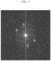
- FIG. 3 shows the Fourier-transformed electron diffraction pattern of the STEM image.
- an interference image by similar electron beams on silicon crystal lattice planes in a particle and an electron beam diffraction pattern of a dot pattern, which is seen in the case of a single crystal, were confirmed. Therefore, it was confirmed that the single-crystal spherical silicon nanoparticles produced in Example 1 were monocrystalline.
- the grating face interval calculated from the obtained electron beam diffraction pattern was 0.162 nm, and it was confirmed that it was an electron beam diffraction pattern from (311) face of crystalline silicon.
- FIG. 4 shows the IR measurement result of the single-crystal spherical silicon nanoparticles of Example 1-2 in the wavenumber range of 1800 cm -1 to 2300 cm -1 . Since the absorption at 2105 cm -1 is attributed to stretching vibration of Si-H bond, it was confirmed that the surface of the single-crystal spherical silicon nanoparticles was hydrogenated. Example 1-1, Example 1-3, and Example 1-4 were also confirmed in the same manner. Since Si-H bond can make the surface of single-crystal spherical silicon nanoparticles hydrophobic, it was confirmed that the single-crystal spherical silicon nanoparticles can be well dispersed in an organic solvent. As shown in FIG. 1 , it was observed that the single-crystal spherical silicon nanoparticles of the present invention were dispersed even at an extremely small distance of around 5 nm.
- FIG. 5a shows the IR spectrum in the wavenumber range of 900 cm -1 to 1300 cm -1 .
- an absorption maximum was confirmed at 1095 cm -1 .
- This absorption peak wavenumber coincides with the absorption peak wavenumber of 1095 cm -1 of amorphous silica (SiO 2 ) as a reagent.
- the IR spectrum of a single-crystal silicon wafer is shown. The absorption maximum of the wafer was confirmed at a wavenumber of 1105 cm -1 , and this was absorption occurred in a state where oxygen was contained between silicon crystal lattices as solid solution.
- FIG. 5b shows the IR spectrum in the wavenumber range of 400 cm -1 to 550 cm -1 .
- any absorption peak with a distinct maximum was not observed, but for the reagent amorphous silica (SiO 2 ), a maximum absorption peak was observed at 460 cm -1 .
- the presence of oxygen that can bond with a silicon atom in silicon crystal be as small as possible. It is desirable that the ratio: B/A is less than 0.2, where A is the peak intensity of the maximum peak observed in the wavenumber range of 1000 cm -1 to 1200 cm -1 , and B is the peak intensity of the maximum peak observed in the wavenumber range of 400 cm -1 to 500 cm -1 in the IR spectrum. In Example 1-4, the ratio: B/A is 0.1, which is less than 0.2. To the contrary, the reagent amorphous silica (SiO 2 ) exhibits the maximum peak at the peak wavenumber of 460 cm -1 , and the ratio: B/A is 0.4, which exceeds 0.2.
- FIG. 5c shows the result of a study of Si-Cl bond, in which a silicon atom and a chlorine atom are bonded.
- Si-Cl bond exists, absorption with a wavenumber that varies depending on the number of chlorine atoms bonded to silicon atoms is observed in the wavenumber range of 530 cm -1 to 630 cm -1 in the IR spectrum.
- Si-Cl bond is likely to be hydrolyzed by atmospheric moisture and lead to production of silicon oxide or hydroxide. Hence, it is desirable to reduce the number of Si-Cl bonds as much as possible.
- the ratio of Si-Cl bond it is desirable that the ratio: C/A is less than 0.2, where A is the peak intensity of the maximum peak observed in the wavenumber range of 1000 cm -1 to 1200 cm -1 and C is the peak intensity of the maximum peak in the wavenumber range of 530 cm -1 to 630 cm -1 .
- the ratio: C/A less than 0.2, even when single-crystal spherical silicon nanoparticles were taken out into the atmosphere, it was not observed that the nanoparticles immediately changed color or changed to silicon oxide or silicon hydroxide.
- the ratio: C/A is 0.06, which is less than 0.2. Similar results were also obtained in Example 1-1 to Example 1-3.
- FIG. 5d shows the IR spectrum in the wavenumber range of 550 cm -1 to 700 cm -1 . It is known that absorption due to substitution of a silicon atom with a carbon atom in silicon crystal occurs in this range. Therefore, the wavenumber range of the absorption due to Si-C bond overlaps with the range of 530 cm -1 to 630 cm -1 of the absorption due to Si-Cl bond described in the previous paragraph. In Example 1-4, the absorption at the wavenumber of 612 cm -1 was explained to be due to Si-Cl bond.
- the carbon concentration is lower than that of the silicon wafer because the ratio: C/A in Example 1-4 is 0.06, which is lower as compared with the ratio: C/A of 0.5 based on the wavenumber of 610 cm -1 confirmed for the silicon wafer. Since the single-crystal spherical silicon nanoparticles of the present invention are produced by reducing silicon halide with a reduction liquid containing an aromatic compound, it was expected that carbon would be contained in single-crystal spherical silicon nanoparticles as an impurity.
- the single-crystal spherical silicon particles of the present invention contain almost no carbon atoms, and are therefore highly pure. Since the absorption wavenumber due to Si-C bond and the absorption wavenumber due to Si-Cl bond overlap, it cannot be unmistakably determined whether the absorption at 612 cm -1 is due to Si-C bond or Si-Cl bond. Still, the single-crystal spherical silicon nanoparticles of Example 1-4 are single-crystal spherical silicon nanoparticles with low concentrations of carbon and chlorine.
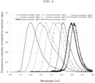
- FIG. 6 shows fluorescence spectra of the single-crystal spherical silicon nanoparticles of Example 1-3. These are fluorescence spectra normalized by setting the maximum intensity of the fluorescence spectrum obtained for each excitation wavelength to 1.0 and are the results of changing the excitation wavelength from 340 nm to 600 nm in steps of 40 nm. From the results in FIG. 6 , it was confirmed that the fluorescence of the single-crystal spherical silicon nanoparticles of Example 1-3 showed maximum peaks in the range of 400 nm to 610 nm depending on the excitation wavelength.
- FIG. 7 was created based on the results of FIG. 6 and shows excitation wavelength dependence of the fluorescence peak wavelength of the single-crystal spherical silicon nanoparticles of Example 1-3. Since it is known that as the particle diameter of silicon nanoparticles increases, the fluorescence peak wavelength shifts to the longer wavelength side, it was confirmed that fluorescence from the nanoparticles reflecting the particle size distribution of the single-crystal spherical silicon nanoparticles was obtained.
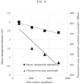
- FIG. 8 shows measurement results of the particle diameter and the fluorescence peak wavelength relative to the disk rotation speed of the single-crystal spherical silicon nanoparticles of Example 1-1 to Example 1-4. It was confirmed that the particle diameter of the single-crystal spherical silicon nanoparticles decreased as the disk rotation speed increased. Therefore, it was confirmed that the particle diameter of single-crystal spherical silicon nanoparticles could be controlled by the disk rotation speed. In addition, it was confirmed that the fluorescence peak wavelength shifted to the shorter wavelength side as the disk rotation speed increased, that is, as the silicon nanoparticle diameter decreased. This change in fluorescence peak wavelength due to particle diameter is explained by (A) quantum effect of the three mechanisms (A) to (C) above.
- FIG. 9 shows the visible light fluorescence spectrum of the single-crystal spherical silicon nanoparticles of Example 1-2 at deep ultraviolet wavelengths.
- Deep ultraviolet light refers to light in the wavelength range of 200 nm to 300 nm.
- visible light fluorescence in the wavelength range of 400 nm to 600 nm with fluorescence peaks at 470 nm and 550 nm could also be obtained by short-wavelength deep ultraviolet light. Similar results were obtained in Example 1-1, Example 1-3, and Example 1-4.
- Table 3 shows the average particle diameter, the circularity, the relative fluorescence quantum efficiency as well as the ratio: B/A and the ratio: C obtained from the IR spectra, of the single-crystal spherical silicon nanoparticles of Example 1-1 to Example 1-4.
- the single-crystal spherical silicon nanoparticles of Example 1-1 to Example 1-4 have the ratio: B/A of 0.08 to 0.10 and the ratio of C/A of 0.06 to 0.08, which are both less than 0.2.
- Example 2 silicon tetrabromide (SiBr 4 ) was used in place of silicon tetrachloride (SiCl 4 ) used in Example 1, and single-crystal spherical silicon nanoparticles were produced by reducing a THF solution of silicon tetrabromide (single-crystal spherical silicon nanoparticle raw material liquid) with a naphthalene-dissolved THF solution of metal lithium (single-crystal spherical silicon nanoparticle reduction liquid).
- Example 4 shows the formulations of Example 2-1 to Example 2-4.
- the solvent used in Example 2 is super dehydrated tetrahydrofuran with a residual water content of 10 ppm or less (FUJIFILM Wako Pure Chemical Corporation), which is the same as in Example 1.
- a single-crystal spherical silicon nanoparticle reduction liquid (Liquid A) and a single-crystal spherical silicon nanoparticle raw material liquid (Liquid B) were prepared in a glove box with an argon atmosphere.
- a dry powder sample and a wet cake sample were prepared from the single-crystal spherical silicon nanoparticle dispersion discharged from the fluid processing apparatus and recovered in a beaker.
- the preparation method was according to a conventional method.
- the discharged single-crystal spherical silicon nanoparticle dispersion was recovered, the single-crystal spherical silicon nanoparticles were sedimented from the recovered liquid by centrifugation (1,000,000G, 4 hours), and the supernatant was removed.
- Table 7 shows the formulations of Comparative Example 1-1 to Example 1-3.
- the THF used in Comparative Example 1 is super dehydrated tetrahydrofuran with a residual water content of 10 ppm or less (FUJIFILM Wako Pure Chemical Corporation), which is the same as in Example 1.
- a silicon nanoparticle reduction liquid (Liquid A) and a silicon nanoparticle raw material liquid (Liquid B) were prepared in a glove box with an argon atmosphere.
- Liquid A the silicon nanoparticle reduction liquid was prepared at room temperature of 16°C to 17°C by measuring 30 mmol of metal lithium in a flask in advance, pouring 200 mL of the THF solution in which 40 mmol of DBB had been dissolved in the flask, and dissolving the metal lithium with a glass-coated magnetic stirrer.
- silicon tetrachloride a silicon nanoparticle raw material for Liquid B, was dissolved in THF, and then stirred for at least 60 minutes with a glass-coated magnetic stirrer.
- SiCl 4 is silicon tetrachloride (Tokyo Chemical Industry Co., Ltd.)
- Li is metal lithium (Kishida Chemical Co., Ltd.)
- C10H8 is naphthalene (Kanto Chemical Co., Ltd.)
- DBB is 4,4'-di-tert-butylbiphenyl (manufactured by Tokyo Chemical Industry Co., Ltd.).
- the silicon nanoparticle dispersion discharged and recovered from the fluid processing apparatus was subjected to the surface stabilization treatment described in Example 6 of Patent Literature 5. Specifically, 10 mL of the silicon nanoparticle dispersion was put in a 100 mL three-necked flask in a glove box with an argon atmosphere, and the flask was kept in a cooling tank maintained at -3°C using IPA as a coolant.
- a solution containing hexylmagnesium bromide (manufactured by Tokyo Chemical Industry Co., Ltd.) at a concentration of four times the molar concentration of silicon in the silicon nanoparticle dispersion was added dropwise to the discharge liquid using a glass syringe with a metal needle passing through a rubber septum of the three-necked flask. After the dropwise addition, the cooling tank was removed, the temperature was gradually raised to room temperature of 16°C to 17°C, and the mixture was stirred for 24 hours under an argon atmosphere.
- hexylmagnesium bromide manufactured by Tokyo Chemical Industry Co., Ltd.
- FIG. 10 shows the STEM image of the hexyl group-terminated silicon nanoparticles prepared Comparative Example 1-1. According to the STEM image, although the hexyl group-terminated silicon particles were crystals, it was observed that the lattice planes therein were not aligned in a certain direction, and it was confirmed that the hexyl group-terminated silicon particles were polycrystals with intersecting lattice planes.
- the silicon nanoparticles were not spherical but had a distorted particle shape.
- the circularity of the hexyl group-terminated silicon nanoparticles of Comparative Example 1-1 to Comparative Example 1-3 was 0.83 or 0.84, not 0.9 or more.
- Example 1 of the present invention the single-crystal spherical silicon nanoparticle reduction liquid was prepared at a temperature of -20°C, but in Comparative Example 1, it was prepared at a room temperature of 16°C to 17°C. This was to match Example 1 of Patent Literature 4 and Example 6 of Patent Literature 5, in which the reduction liquid was prepared from metal lithium and DBB at room temperature.
- a DBB anion is produced by a transfer of an electron generated when metal lithium is dissolved in THF as a lithium ion to DBB.
- a DBB anion and a lithium ion can exist with THF therebetween, but when the temperature during the liquid preparation is 0°C or more, a DBB anion can form an ionic bond directly with a lithium ion with no THF therebetween.
- a chlorine atom was in a state of being bonded to the surface of silicon nanoparticles in order to be subjected to surface stabilization treatment with a hexyl group. Therefore, the number of moles of metal lithium, a reducing agent, was set to 3/4 times the number of moles of silicon tetrachloride. This was to match the molar ratio of the metal lithium in Example 1 of Patent Literature 4 and Example 6 of Patent Literature 5.
- the silicon nanoparticles before the surface stabilization treatment differ from the single-crystal spherical silicon nanoparticles of the present invention in that the surface is intentionally chlorinated.
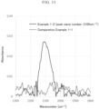
- FIG. 11 shows the IR spectrum of the polycrystalline silicon nanoparticles of Comparative Example 1-1 in the wavenumber range of 1800 cm -1 to 2300 cm -1 .
- Comparative Example 1-1 the absorption peak due to Si-H bond near 2100 cm -1 confirmed in Example 1-2 was not observed.
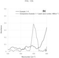
- FIG. 12a and FIG. 12b show the IR spectra of the polycrystalline silicon nanoparticles of Comparative Example 1-1.
- Example 1-4 an absorption peak with a wide spectrum width was observed at 1095 cm -1 , but in Comparative Example 1-1, an absorption peak with a narrow spectral width was observed at 1084 cm -1 .
- an absorption peak was also observed at 450 cm -1 on the low wavenumber side.
- FIG. 12c shows the IR spectrum of the polycrystalline silicon nanoparticles of Comparative Example 1-1 in the wavenumber range of 450 cm -1 to 650 cm -1 .
- a distinct maximum absorption peak was observed at 620 cm -1 , thereby confirming the presence of Si-Cl bond.
- the ratio: C/A is 0.25, not less than 0.2, where A is the peak intensity of the maximum peak observed in the wavenumber range of 1000 cm -1 to 1200 cm -1 and C is the peak intensity of the maximum peak observed in the wavenumber range of 530 cm -1 to 630 cm -1 in the IR spectrum.
- FIG. 12d shows the IR spectrum of the polycrystalline silicon nanoparticles of Comparative Example 1-1 in the wavenumber range of 550 cm -1 to 700 cm -1 .
- an absorption peak with an absorbance of 0.25 was observed at 620 cm -1 .
- this wavenumber range overlaps with the range of 530 cm -1 to 630 cm -1 in which absorption occurs even when a silicon atom formed a bond with a chlorine atom.
- the ratio: C/A is 0.25, not less than 0.2.
- the polycrystalline silicon nanoparticles of Comparative Example 1-1 exhibited maximum fluorescence in the wavelength range of 400 nm to 600 nm.
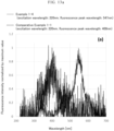
- FIG. 13a and FIG. 13b it was confirmed that the fluorescence spectrum of the polycrystalline silicon nanoparticles of Comparative Example 1-1 by deep ultraviolet light with an excitation light wavelength of 300 nm or less showed a fluorescence peak at a wavelength of 400 nm or less, and it was observed that the fluorescence spectra of the polycrystalline silicon nanoparticles of Comparative Example 1-2 and Comparative Example 1-3 upon excitation by deep ultraviolet light similarly showed a peak at 400 nm or less.
- Example 1-4 results were different from the results in Example 1-4 in which the fluorescence peak wavelength was 547 nm for excitation wavelength of 220 nm and the fluorescence peak was 568 nm for excitation wavelength of 260 nm. Since the fluorescence peak wavelengths due to excitation by deep ultraviolet light of the polycrystalline silicon nanoparticles in Comparative Example 1-1 to Comparative Example 1-3 were all 400 nm or less, it was confirmed that the polycrystalline silicon nanoparticles had an electron energy structure different from that of the single-crystal spherical silicon nanoparticles which showed a fluorescence peak in a visible light range of 400 nm to 600 nm.
- the silicon nanoparticles of Comparative Example 1 are each a polycrystal which is an aggregate of single crystals with different crystallite diameters, electron energy levels for absorption of excitation light and for fluorescence emission are different from those of the single-crystal spherical silicon nanoparticles.
- this is because since the diameter of the silicon particles prepared in Examples and Comparative Examples was around 5 nm, a slight change in crystallite diameter had a large effect on the size of the band gap of silicon, and because a polycrystal includes grain boundaries where crystallites of each single crystal are in contact with each other, so that an electron energy level due to the presence of the grain boundaries exists.
- Table 9 shows the average particle diameter, the circularity, the relative fluorescence quantum efficiency as well as the ratio: B/A and the ratio: C obtained from the IR spectra, of the polycrystalline silicon nanoparticles of Comparative Example 1-1 to Comparative Example 1-3.
- the silicon nanoparticles of Comparative Example 1 were polycrystalline silicon nanoparticles, and the values of the ratio: B/A and the ratio: C/A are 0.2 or more. It was confirmed that these values were different when compared to the ratio: B/A and the ratio: C/A of the single-crystal spherical silicon nanoparticles of Example 1 and Example 2.
- Table 10 shows the formulations in Example 3-1 and Example 3-2.
- Table 11 shows the operation conditions of the fluid processing apparatus in Example 3-1 and Example 3-2.
- Table 9 shows the average particle diameter, the circularity, the relative fluorescence quantum efficiency as well as the ratio: B/A and the ratio: C obtained from the IR spectra, of the single-crystal spherical silicon nanoparticles of Example 3-1 and Example 3-2.
- the relative fluorescence quantum efficiency was 11% to 13%.
- the values of the ratio: B/A and the ratio: C/A of the silicon nanoparticles of Example 3 are 0.1 or less. It was confirmed that these values were equivalent to the ratio: B/A and the ratio: C/A of the single-crystal spherical silicon nanoparticles of Example 1 and Example 2.
- Table 13 shows the formulations in Example 4-1 and Example 4-2.
- Table 14 shows the operation conditions of the fluid processing apparatus in Example 4-1 and Example 4-2.
- Table 15 shows the average particle diameter, the circularity, the relative fluorescence quantum efficiency as well as the ratio: B/A and the ratio: C obtained from the IR spectra, of the single-crystal spherical silicon nanoparticles of Example 4-1 and Example 4-2.
- Table 16 shows the formulations of Comparative Example 2-1 and Comparative Example 2-2.
- Table 17 shows the operation conditions of the fluid processing apparatus in Comparative Example 2-1 and Comparative Example 2-2.
- the alkali metal in the reduction liquid was metal lithium, and the temperature of the reduction liquid of Liquid A was set to 25°C.
- the disk rotation speed was set to 3500 rpm and 5000 rpm.
- Table 18 shows the average particle diameter, the circularity, the relative fluorescence quantum efficiency as well as the ratio: B/A and the ratio: C/A obtained from the IR spectra, of the single-crystal spherical silicon nanoparticles of Comparative Example 2-1 and Comparative Example 2-2.
- the average particle diameter was as large as 4 nm or more even when the disk rotation speed was high, and the relative fluorescence quantum efficiency decreased to less than 5%. It was confirmed that the values of the ratio: B/A and the ratio: C/A were different from and larger than the ratio: B/A and the ratio: C/A of the single-crystal spherical silicon nanoparticles of Example 1 to Example 4.
- Table 19 shows the formulations of Comparative Example 3-1 and Comparative Example 3-2.
- Table 20 shows the operation conditions of the fluid processing apparatus in Comparative Example 3-1 and Comparative Example 3-2.
- the alkali metal in the reduction liquid of Liquid A was metal lithium, and the temperature of the reduction liquid was kept at 5°C.
- Table 21 shows the average particle diameter, the circularity, the relative fluorescence quantum efficiency as well as the ratio: B/A and the ratio: C/A obtained from the IR spectra, of the single-crystal spherical silicon nanoparticles of Comparative Example 3-1 and Comparative Example 3-2.
- the single-crystal spherical silicon nanoparticles of the present invention are each a single crystal with no grain boundaries that reduce fluorescence efficiency, they can produce fluorescence at a high fluorescence quantum efficiency upon excitation by light in a wide range of wavelengths from deep ultraviolet light having a wavelength of 200 nm to 300 nm to visible light, and can increase the conventionally known fluorescence quantum efficiency of silicon nanoparticles from around 1% to 10% or more.
Landscapes
- Chemical & Material Sciences (AREA)
- Organic Chemistry (AREA)
- Engineering & Computer Science (AREA)
- Materials Engineering (AREA)
- Crystallography & Structural Chemistry (AREA)
- Metallurgy (AREA)
- Inorganic Chemistry (AREA)
- Chemical Kinetics & Catalysis (AREA)
- General Chemical & Material Sciences (AREA)
- Crystals, And After-Treatments Of Crystals (AREA)
- Silicon Compounds (AREA)
Applications Claiming Priority (1)
| Application Number | Priority Date | Filing Date | Title |
|---|---|---|---|
| PCT/JP2022/020113 WO2023218617A1 (ja) | 2022-05-12 | 2022-05-12 | 単結晶球状シリコンナノ粒子 |
Publications (2)
| Publication Number | Publication Date |
|---|---|
| EP4524104A1 true EP4524104A1 (de) | 2025-03-19 |
| EP4524104A4 EP4524104A4 (de) | 2026-02-25 |
Family
ID=88729928
Family Applications (2)
| Application Number | Title | Priority Date | Filing Date |
|---|---|---|---|
| EP22941696.1A Pending EP4524104A4 (de) | 2022-05-12 | 2022-05-12 | Sphärische einkristall-siliciumnanopartikel |
| EP22941749.8A Pending EP4524095A4 (de) | 2022-05-12 | 2022-05-19 | Herstellungsverfahren für sphärische einkristall-siliciumnanopartikel |
Family Applications After (1)
| Application Number | Title | Priority Date | Filing Date |
|---|---|---|---|
| EP22941749.8A Pending EP4524095A4 (de) | 2022-05-12 | 2022-05-19 | Herstellungsverfahren für sphärische einkristall-siliciumnanopartikel |
Country Status (6)
| Country | Link |
|---|---|
| US (2) | US20250333876A1 (de) |
| EP (2) | EP4524104A4 (de) |
| JP (1) | JPWO2023218617A1 (de) |
| KR (2) | KR102779630B1 (de) |
| CN (2) | CN117396434A (de) |
| WO (2) | WO2023218617A1 (de) |
Families Citing this family (1)
| Publication number | Priority date | Publication date | Assignee | Title |
|---|---|---|---|---|
| JPWO2023218617A1 (de) * | 2022-05-12 | 2023-11-16 |
Family Cites Families (23)
| Publication number | Priority date | Publication date | Assignee | Title |
|---|---|---|---|---|
| EP1427873A1 (de) | 2001-09-19 | 2004-06-16 | Evergreen Solar Inc. | Verfahren mit hohe ausbeute zur herstellung von siliciumnanokristallen mit chemisch-zugänglichen oberflächen |
| US9402791B1 (en) * | 2004-03-30 | 2016-08-02 | James Beckman | Ultra-violet radiation absorbing silicon particle nanoclusters |
| JP4504267B2 (ja) | 2005-06-28 | 2010-07-14 | 株式会社東芝 | 半導体ナノ粒子の製造方法及び半導体材料の表面を被覆する方法 |
| JP2009504423A (ja) * | 2005-08-11 | 2009-02-05 | イノヴァライト インコーポレイテッド | 安定にパッシベートされたiv族半導体ナノ粒子、並びにその製造方法及びその組成物 |
| EP1760045A1 (de) * | 2005-09-03 | 2007-03-07 | Degussa GmbH | Nanoskalige Siliziumteilchen |
| JP2007197382A (ja) | 2006-01-27 | 2007-08-09 | Konica Minolta Medical & Graphic Inc | 半導体ナノ粒子 |
| WO2007120871A2 (en) * | 2006-04-13 | 2007-10-25 | Cabot Corporation | Production of silicon through a closed-loop process |
| WO2009011981A2 (en) * | 2007-05-31 | 2009-01-22 | The Administrators Of The Tulane Educational Fund | Method of forming stable functionalized nanoparticles |
| JP4458202B2 (ja) | 2007-08-09 | 2010-04-28 | エム・テクニック株式会社 | 半導体微粒子の製造方法 |
| JP5648986B2 (ja) | 2007-11-02 | 2015-01-07 | エム・テクニック株式会社 | 流体処理装置及び流体処理方法 |
| CN101439859B (zh) * | 2008-12-02 | 2011-08-03 | 浙江大学 | 一种绿色荧光纳米硅晶体 |
| KR101053836B1 (ko) * | 2009-02-10 | 2011-08-03 | 한국에너지기술연구원 | Icp를 이용한 실리콘 나노입자 제조 장치 |
| JP5598809B2 (ja) | 2009-03-06 | 2014-10-01 | 独立行政法人物質・材料研究機構 | 発光素子 |
| JP6057424B2 (ja) | 2013-03-06 | 2017-01-11 | 学校法人東京電機大学 | シリコンナノ粒子の製造方法 |
| JP2015201621A (ja) * | 2014-04-03 | 2015-11-12 | 国立研究開発法人物質・材料研究機構 | 発光性シリコンナノ粒子及び電流注入型発光素子 |
| JP6520245B2 (ja) * | 2015-03-12 | 2019-05-29 | 日本製鉄株式会社 | シリコンナノ粒子発光体の製造方法およびそのシリコンナノ粒子発光体を用いた発光素子 |
| JP6632052B2 (ja) * | 2015-05-18 | 2020-01-15 | 国立大学法人群馬大学 | 発光シリコン粒子及び発光シリコン粒子の製造方法 |
| EP3323788A4 (de) | 2015-07-14 | 2019-02-20 | M. Technique Co., Ltd. | Verfahren zur herstellung von oxidpartikeln |
| JP6614651B2 (ja) | 2015-10-23 | 2019-12-04 | 学校法人慶應義塾 | シリコンナノ粒子の製造方法及び装置 |
| CN107265462A (zh) * | 2017-05-05 | 2017-10-20 | 北京大学 | 一种由四卤化硅制备纳米硅的方法 |
| US20190071794A1 (en) | 2017-09-01 | 2019-03-07 | Sri International | Efficient solar grade silicon production system |
| JP7108160B2 (ja) * | 2018-03-09 | 2022-07-28 | 学校法人法政大学 | シリコン量子ドットの製造方法 |
| JPWO2023218617A1 (de) * | 2022-05-12 | 2023-11-16 |
-
2022
- 2022-05-12 JP JP2023545770A patent/JPWO2023218617A1/ja active Pending
- 2022-05-12 EP EP22941696.1A patent/EP4524104A4/de active Pending
- 2022-05-12 CN CN202280037575.3A patent/CN117396434A/zh active Pending
- 2022-05-12 WO PCT/JP2022/020113 patent/WO2023218617A1/ja not_active Ceased
- 2022-05-12 US US18/288,302 patent/US20250333876A1/en active Pending
- 2022-05-12 KR KR1020237034013A patent/KR102779630B1/ko active Active
- 2022-05-19 US US18/287,583 patent/US20250333875A1/en active Pending
- 2022-05-19 EP EP22941749.8A patent/EP4524095A4/de active Pending
- 2022-05-19 WO PCT/JP2022/020825 patent/WO2023218673A1/ja not_active Ceased
- 2022-05-19 CN CN202280035206.0A patent/CN117396433B/zh active Active
- 2022-05-19 KR KR1020237034014A patent/KR102756301B1/ko active Active
Also Published As
| Publication number | Publication date |
|---|---|
| CN117396433A (zh) | 2024-01-12 |
| EP4524104A4 (de) | 2026-02-25 |
| US20250333875A1 (en) | 2025-10-30 |
| WO2023218617A1 (ja) | 2023-11-16 |
| KR102756301B1 (ko) | 2025-01-21 |
| KR20230159458A (ko) | 2023-11-21 |
| EP4524095A1 (de) | 2025-03-19 |
| JPWO2023218673A1 (de) | 2023-11-16 |
| KR20230159459A (ko) | 2023-11-21 |
| CN117396434A (zh) | 2024-01-12 |
| US20250333876A1 (en) | 2025-10-30 |
| KR102779630B1 (ko) | 2025-03-12 |
| WO2023218673A1 (ja) | 2023-11-16 |
| JPWO2023218617A1 (de) | 2023-11-16 |
| EP4524095A4 (de) | 2026-05-20 |
| CN117396433B (zh) | 2026-04-10 |
Similar Documents
| Publication | Publication Date | Title |
|---|---|---|
| Zheng et al. | Aqueous synthesis of glutathione‐capped ZnSe and Zn1–xCdxSe alloyed quantum dots | |
| US7371666B2 (en) | Process for producing luminescent silicon nanoparticles | |
| Ahmad et al. | Zinc oxalate nanorods: a convenient precursor to uniform nanoparticles of ZnO | |
| EP0581621B1 (de) | Neue grüne Lanthan-Terbium und Ceriumphosphat-Gemischsleuchtstoffe, Vorläufer davon und Verfahren zur Herstellung | |
| EP4524095A1 (de) | Herstellungsverfahren für sphärische einkristall-siliciumnanopartikel | |
| JP5446052B2 (ja) | 酸化亜鉛超微粒子分散溶液、及び該酸化亜鉛超微粒子分散溶液の製造方法、並びに酸化亜鉛薄膜 | |
| JP7862018B2 (ja) | 単結晶球状シリコンナノ粒子の製造方法 | |
| EP4588892A1 (de) | Herstellungsverfahren für sphärische einkristall-kohlenstoffnanopartikel | |
| JP5131195B2 (ja) | 半導体ナノ粒子とその製造方法 | |
| US20060046447A1 (en) | Method for coating semiconductor surface, process for production of semiconductor particles using said method, and optical element using said semiconductor particles | |
| Shiba et al. | Preparation of Eu (III) acetylacetonate-doped well-defined titania particles with efficient photoluminescence properties | |
| WO2007002539A2 (en) | Nanoparticles and method of making thereof | |
| WO2024224517A1 (ja) | 単結晶球状金属ナトリウムナノ粒子の製造方法 | |
| KR20250142909A (ko) | 백금 담지 단결정 구상 카본 나노입자의 제조방법 | |
| López et al. | Structural and optical properties of SiOx films deposited by HFCVD | |
| CN118256226A (zh) | 一种红光钙钛矿量子点溶液的制备方法及其应用 | |
| Devi et al. | Structural, Compositional and Optical Properties of PVA-capped Nanocrystalline CdSe Thin Films Prepared by Chemical Bath Deposition | |
| Sakohara et al. | Preparation and optical properties of nano-sized ZnO colloidal particles using NH3 gas as volatile catalyst | |
| Ca et al. | Synthesis, structure, and spectroscopic properties of Dy3+-doped ZnSe quantum dots: Judd–Ofelt analysis, energy transfer, and thermal stability | |
| EP4321277A1 (de) | Mit siliciumverbindungen beschichtete metall-magnesium-partikel | |
| RU2672160C2 (ru) | Способ получения дисперсии 2d-наномонокристаллов кремния в органическом растворителе для фотовольтаических применений | |
| Lin et al. | Rare Earth Doped Yttrium Oxide Nanophosphors Synthesis and Engineering-Controllable Photoluminescence Properties |
Legal Events
| Date | Code | Title | Description |
|---|---|---|---|
| STAA | Information on the status of an ep patent application or granted ep patent |
Free format text: STATUS: THE INTERNATIONAL PUBLICATION HAS BEEN MADE |
|
| PUAI | Public reference made under article 153(3) epc to a published international application that has entered the european phase |
Free format text: ORIGINAL CODE: 0009012 |
|
| STAA | Information on the status of an ep patent application or granted ep patent |
Free format text: STATUS: REQUEST FOR EXAMINATION WAS MADE |
|
| 17P | Request for examination filed |
Effective date: 20231130 |
|
| AK | Designated contracting states |
Kind code of ref document: A1 Designated state(s): AL AT BE BG CH CY CZ DE DK EE ES FI FR GB GR HR HU IE IS IT LI LT LU LV MC MK MT NL NO PL PT RO RS SE SI SK SM TR |
|
| DAV | Request for validation of the european patent (deleted) | ||
| DAX | Request for extension of the european patent (deleted) | ||
| A4 | Supplementary search report drawn up and despatched |
Effective date: 20260128 |
|
| RIC1 | Information provided on ipc code assigned before grant |
Ipc: C01B 33/18 20060101AFI20260122BHEP Ipc: B82B 1/00 20060101ALI20260122BHEP Ipc: B82Y 20/00 20110101ALI20260122BHEP Ipc: C09K 11/59 20060101ALI20260122BHEP Ipc: C01B 33/021 20060101ALI20260122BHEP Ipc: C01B 33/023 20060101ALI20260122BHEP Ipc: C30B 7/14 20060101ALI20260122BHEP Ipc: C30B 29/06 20060101ALI20260122BHEP Ipc: C30B 29/60 20060101ALI20260122BHEP Ipc: H10F 77/45 20250101ALI20260122BHEP Ipc: H10H 20/01 20250101ALI20260122BHEP Ipc: H10H 20/851 20250101ALI20260122BHEP Ipc: C01B 33/02 20060101ALI20260122BHEP Ipc: B82Y 40/00 20110101ALI20260122BHEP Ipc: H10H 29/851 20250101ALI20260122BHEP |