EP4524282A2 - Procédé de revêtement de surface par pulvérisation cathodique - Google Patents
Procédé de revêtement de surface par pulvérisation cathodique Download PDFInfo
- Publication number
- EP4524282A2 EP4524282A2 EP24192386.1A EP24192386A EP4524282A2 EP 4524282 A2 EP4524282 A2 EP 4524282A2 EP 24192386 A EP24192386 A EP 24192386A EP 4524282 A2 EP4524282 A2 EP 4524282A2
- Authority
- EP
- European Patent Office
- Prior art keywords
- carrier gas
- vacuum chamber
- source
- sputtering
- gas flow
- Prior art date
- Legal status (The legal status is an assumption and is not a legal conclusion. Google has not performed a legal analysis and makes no representation as to the accuracy of the status listed.)
- Pending
Links
Images


Classifications
-
- C—CHEMISTRY; METALLURGY
- C23—COATING METALLIC MATERIAL; COATING MATERIAL WITH METALLIC MATERIAL; CHEMICAL SURFACE TREATMENT; DIFFUSION TREATMENT OF METALLIC MATERIAL; COATING BY VACUUM EVAPORATION, BY SPUTTERING, BY ION IMPLANTATION OR BY CHEMICAL VAPOUR DEPOSITION, IN GENERAL; INHIBITING CORROSION OF METALLIC MATERIAL OR INCRUSTATION IN GENERAL
- C23C—COATING METALLIC MATERIAL; COATING MATERIAL WITH METALLIC MATERIAL; SURFACE TREATMENT OF METALLIC MATERIAL BY DIFFUSION INTO THE SURFACE, BY CHEMICAL CONVERSION OR SUBSTITUTION; COATING BY VACUUM EVAPORATION, BY SPUTTERING, BY ION IMPLANTATION OR BY CHEMICAL VAPOUR DEPOSITION, IN GENERAL
- C23C14/00—Coating by vacuum evaporation, by sputtering or by ion implantation of the coating forming material
- C23C14/0021—Reactive sputtering or evaporation
- C23C14/0036—Reactive sputtering
-
- C—CHEMISTRY; METALLURGY
- C23—COATING METALLIC MATERIAL; COATING MATERIAL WITH METALLIC MATERIAL; CHEMICAL SURFACE TREATMENT; DIFFUSION TREATMENT OF METALLIC MATERIAL; COATING BY VACUUM EVAPORATION, BY SPUTTERING, BY ION IMPLANTATION OR BY CHEMICAL VAPOUR DEPOSITION, IN GENERAL; INHIBITING CORROSION OF METALLIC MATERIAL OR INCRUSTATION IN GENERAL
- C23C—COATING METALLIC MATERIAL; COATING MATERIAL WITH METALLIC MATERIAL; SURFACE TREATMENT OF METALLIC MATERIAL BY DIFFUSION INTO THE SURFACE, BY CHEMICAL CONVERSION OR SUBSTITUTION; COATING BY VACUUM EVAPORATION, BY SPUTTERING, BY ION IMPLANTATION OR BY CHEMICAL VAPOUR DEPOSITION, IN GENERAL
- C23C14/00—Coating by vacuum evaporation, by sputtering or by ion implantation of the coating forming material
- C23C14/22—Coating by vacuum evaporation, by sputtering or by ion implantation of the coating forming material characterised by the process of coating
- C23C14/34—Sputtering
- C23C14/3407—Cathode assembly for sputtering apparatus, e.g. Target
-
- C—CHEMISTRY; METALLURGY
- C23—COATING METALLIC MATERIAL; COATING MATERIAL WITH METALLIC MATERIAL; CHEMICAL SURFACE TREATMENT; DIFFUSION TREATMENT OF METALLIC MATERIAL; COATING BY VACUUM EVAPORATION, BY SPUTTERING, BY ION IMPLANTATION OR BY CHEMICAL VAPOUR DEPOSITION, IN GENERAL; INHIBITING CORROSION OF METALLIC MATERIAL OR INCRUSTATION IN GENERAL
- C23C—COATING METALLIC MATERIAL; COATING MATERIAL WITH METALLIC MATERIAL; SURFACE TREATMENT OF METALLIC MATERIAL BY DIFFUSION INTO THE SURFACE, BY CHEMICAL CONVERSION OR SUBSTITUTION; COATING BY VACUUM EVAPORATION, BY SPUTTERING, BY ION IMPLANTATION OR BY CHEMICAL VAPOUR DEPOSITION, IN GENERAL
- C23C14/00—Coating by vacuum evaporation, by sputtering or by ion implantation of the coating forming material
- C23C14/22—Coating by vacuum evaporation, by sputtering or by ion implantation of the coating forming material characterised by the process of coating
- C23C14/34—Sputtering
- C23C14/3435—Applying energy to the substrate during sputtering
-
- C—CHEMISTRY; METALLURGY
- C23—COATING METALLIC MATERIAL; COATING MATERIAL WITH METALLIC MATERIAL; CHEMICAL SURFACE TREATMENT; DIFFUSION TREATMENT OF METALLIC MATERIAL; COATING BY VACUUM EVAPORATION, BY SPUTTERING, BY ION IMPLANTATION OR BY CHEMICAL VAPOUR DEPOSITION, IN GENERAL; INHIBITING CORROSION OF METALLIC MATERIAL OR INCRUSTATION IN GENERAL
- C23C—COATING METALLIC MATERIAL; COATING MATERIAL WITH METALLIC MATERIAL; SURFACE TREATMENT OF METALLIC MATERIAL BY DIFFUSION INTO THE SURFACE, BY CHEMICAL CONVERSION OR SUBSTITUTION; COATING BY VACUUM EVAPORATION, BY SPUTTERING, BY ION IMPLANTATION OR BY CHEMICAL VAPOUR DEPOSITION, IN GENERAL
- C23C14/00—Coating by vacuum evaporation, by sputtering or by ion implantation of the coating forming material
- C23C14/22—Coating by vacuum evaporation, by sputtering or by ion implantation of the coating forming material characterised by the process of coating
- C23C14/34—Sputtering
- C23C14/3485—Sputtering using pulsed power to the target
-
- C—CHEMISTRY; METALLURGY
- C23—COATING METALLIC MATERIAL; COATING MATERIAL WITH METALLIC MATERIAL; CHEMICAL SURFACE TREATMENT; DIFFUSION TREATMENT OF METALLIC MATERIAL; COATING BY VACUUM EVAPORATION, BY SPUTTERING, BY ION IMPLANTATION OR BY CHEMICAL VAPOUR DEPOSITION, IN GENERAL; INHIBITING CORROSION OF METALLIC MATERIAL OR INCRUSTATION IN GENERAL
- C23C—COATING METALLIC MATERIAL; COATING MATERIAL WITH METALLIC MATERIAL; SURFACE TREATMENT OF METALLIC MATERIAL BY DIFFUSION INTO THE SURFACE, BY CHEMICAL CONVERSION OR SUBSTITUTION; COATING BY VACUUM EVAPORATION, BY SPUTTERING, BY ION IMPLANTATION OR BY CHEMICAL VAPOUR DEPOSITION, IN GENERAL
- C23C14/00—Coating by vacuum evaporation, by sputtering or by ion implantation of the coating forming material
- C23C14/22—Coating by vacuum evaporation, by sputtering or by ion implantation of the coating forming material characterised by the process of coating
- C23C14/34—Sputtering
- C23C14/3492—Variation of parameters during sputtering
-
- C—CHEMISTRY; METALLURGY
- C23—COATING METALLIC MATERIAL; COATING MATERIAL WITH METALLIC MATERIAL; CHEMICAL SURFACE TREATMENT; DIFFUSION TREATMENT OF METALLIC MATERIAL; COATING BY VACUUM EVAPORATION, BY SPUTTERING, BY ION IMPLANTATION OR BY CHEMICAL VAPOUR DEPOSITION, IN GENERAL; INHIBITING CORROSION OF METALLIC MATERIAL OR INCRUSTATION IN GENERAL
- C23C—COATING METALLIC MATERIAL; COATING MATERIAL WITH METALLIC MATERIAL; SURFACE TREATMENT OF METALLIC MATERIAL BY DIFFUSION INTO THE SURFACE, BY CHEMICAL CONVERSION OR SUBSTITUTION; COATING BY VACUUM EVAPORATION, BY SPUTTERING, BY ION IMPLANTATION OR BY CHEMICAL VAPOUR DEPOSITION, IN GENERAL
- C23C14/00—Coating by vacuum evaporation, by sputtering or by ion implantation of the coating forming material
- C23C14/22—Coating by vacuum evaporation, by sputtering or by ion implantation of the coating forming material characterised by the process of coating
- C23C14/34—Sputtering
- C23C14/35—Sputtering by application of a magnetic field, e.g. magnetron sputtering
- C23C14/352—Sputtering by application of a magnetic field, e.g. magnetron sputtering using more than one target
-
- C—CHEMISTRY; METALLURGY
- C23—COATING METALLIC MATERIAL; COATING MATERIAL WITH METALLIC MATERIAL; CHEMICAL SURFACE TREATMENT; DIFFUSION TREATMENT OF METALLIC MATERIAL; COATING BY VACUUM EVAPORATION, BY SPUTTERING, BY ION IMPLANTATION OR BY CHEMICAL VAPOUR DEPOSITION, IN GENERAL; INHIBITING CORROSION OF METALLIC MATERIAL OR INCRUSTATION IN GENERAL
- C23C—COATING METALLIC MATERIAL; COATING MATERIAL WITH METALLIC MATERIAL; SURFACE TREATMENT OF METALLIC MATERIAL BY DIFFUSION INTO THE SURFACE, BY CHEMICAL CONVERSION OR SUBSTITUTION; COATING BY VACUUM EVAPORATION, BY SPUTTERING, BY ION IMPLANTATION OR BY CHEMICAL VAPOUR DEPOSITION, IN GENERAL
- C23C14/00—Coating by vacuum evaporation, by sputtering or by ion implantation of the coating forming material
- C23C14/22—Coating by vacuum evaporation, by sputtering or by ion implantation of the coating forming material characterised by the process of coating
- C23C14/54—Controlling or regulating the coating process
-
- H—ELECTRICITY
- H01—ELECTRIC ELEMENTS
- H01J—ELECTRIC DISCHARGE TUBES OR DISCHARGE LAMPS
- H01J37/00—Discharge tubes with provision for introducing objects or material to be exposed to the discharge, e.g. for the purpose of examination or processing thereof
- H01J37/32—Gas-filled discharge tubes
- H01J37/32431—Constructional details of the reactor
- H01J37/3244—Gas supply means
- H01J37/32449—Gas control, e.g. control of the gas flow
-
- H—ELECTRICITY
- H01—ELECTRIC ELEMENTS
- H01J—ELECTRIC DISCHARGE TUBES OR DISCHARGE LAMPS
- H01J37/00—Discharge tubes with provision for introducing objects or material to be exposed to the discharge, e.g. for the purpose of examination or processing thereof
- H01J37/32—Gas-filled discharge tubes
- H01J37/34—Gas-filled discharge tubes operating with cathodic sputtering
- H01J37/3402—Gas-filled discharge tubes operating with cathodic sputtering using supplementary magnetic fields
- H01J37/3405—Magnetron sputtering
-
- H—ELECTRICITY
- H01—ELECTRIC ELEMENTS
- H01J—ELECTRIC DISCHARGE TUBES OR DISCHARGE LAMPS
- H01J37/00—Discharge tubes with provision for introducing objects or material to be exposed to the discharge, e.g. for the purpose of examination or processing thereof
- H01J37/32—Gas-filled discharge tubes
- H01J37/34—Gas-filled discharge tubes operating with cathodic sputtering
- H01J37/3411—Constructional aspects of the reactor
- H01J37/3414—Targets
- H01J37/3417—Arrangements
-
- H—ELECTRICITY
- H01—ELECTRIC ELEMENTS
- H01J—ELECTRIC DISCHARGE TUBES OR DISCHARGE LAMPS
- H01J37/00—Discharge tubes with provision for introducing objects or material to be exposed to the discharge, e.g. for the purpose of examination or processing thereof
- H01J37/32—Gas-filled discharge tubes
- H01J37/34—Gas-filled discharge tubes operating with cathodic sputtering
- H01J37/3464—Operating strategies
Definitions
- the invention relates to a method for surface coating according to the sputtering principle with a plasma coating device.
- a solid material called a target which can be a metal, for example, is vaporized, creating a plasma to deposit particles of the solid material onto a substrate, thereby coating the substrate.
- a plasma coating device for surface coating according to the sputtering principle has a vacuum chamber which is evacuated by a vacuum pump and in which the substrate to be coated is placed. At least one sputtering source is arranged in the vacuum chamber, which has a target made of a solid material.
- sputtering is performed using a carrier gas supplied to the vacuum chamber.
- the carrier gas is usually a noble gas, such as argon.
- the plasma treatment device has at least one carrier gas source leading into the vacuum chamber, which generates a carrier gas stream directed toward the sputtering source.
- a plasma is generated from atoms of the carrier gas in the area of the target.
- the ions of the plasma release particles from the solid material of the target.
- the released particles are delivered to the surface of the substrate as a preferably directed particle stream, so that the particles are deposited on a surface of the substrate and form a layer there.
- Coating surfaces using the sputtering principle typically requires low pressure in the coating chamber, i.e., within the vacuum chamber, to enable collision-free transport of the generated vapor to the substrate. Higher pressures lead to the formation of larger particles and scattering of the vapor in all directions, thus resulting in material loss.
- Gas flow sputtering using a carrier gas is used, for example, in DE 42 10 125 C2
- arc evaporation is also used for coating in the prior art. This process advantageously generates a stream of charged particles, which leads to improved coating properties and increased coating adhesion during the coating process.
- EP 1 038 045 B1 a process known as high-power pulsed magnetron sputtering (HIPIMS), in which an electrical modulation of the discharge is carried out with the aim of increasing the current density and thus the degree of ionization.
- HIPIMS high-power pulsed magnetron sputtering
- EP 1 038 045 B1 describes the discontinuous supply of a reactive gas to the vacuum pump in a modulated manner.
- the object of the invention is to provide an improved method for surface coating according to the principle of gas flow sputtering with a high deposition rate.
- the vacuum chamber is evacuated, and a carrier gas stream is supplied from the carrier gas source to the target in such a way that a plasma containing ions composed of atoms of the carrier gas is generated within the vacuum chamber in the region of the target ("gas flow sputtering").
- the plasma ions release particles from the solid material of the target, and the released particles are delivered to the surface of the substrate as a particle stream, preferably in a directed manner. The released particles are thereby deposited on the surface of the substrate and form a layer there.
- the special feature of the invention is that the carrier gas flow is supplied discontinuously to the target of the sputtering source by modulating the gas flow of the carrier gas flow.
- the carrier gas is thus supplied with a modulated gas flow.
- the carrier gas flow is supplied continuously, i.e., at a continuous gas flow rate, and to increase the rate, the continuous gas flow rate is increased
- the gas flow of the carrier gas is to be modulated, i.e., it varies over time.
- the carrier gas flow averaged over time, i.e., the average gas flow is then lower than the carrier gas flow during certain time periods of the modulation.
- the time periods with an increased gas flow of the carrier gas flow compared to the average gas flow are referred to herein as "peaks."
- a peak increases the material input onto the substrate to be coated because the gas flow of the carrier gas is increased during a peak.
- the invention is based on the surprising finding, unexpected by a person skilled in the art, that the deposition rate, i.e., the material input onto the substrate, is overall higher with a modulated carrier gas flow than with a continuous carrier gas flow whose gas flow corresponds to the average carrier gas flow of the modulated gas flow.
- the invention thus provides the crucial advantage that, by modulating the carrier gas flow, the deposition rate onto the substrate can be increased without increasing the average velocity or the average gas flow of the carrier gas flow. Rather, an increased gas flow is only sufficient during individual, recurring peaks, while the average gas flow can remain unchanged or only slightly increased.
- Supplying a carrier gas stream is a mandatory component of gas flow sputtering in order to generate a plasma from the carrier gas, which releases particles from the target.
- a carrier gas is typically a noble gas, such as argon. This must be distinguished from supplying a reactive gas, which is known from the prior art, so that the reactive gas reacts with the plasma generated from the carrier gas. Modulating a reactive gas stream supplied to the vacuum chamber is not the subject of the invention.
- the carrier gas flow can be modulated by switching one or more valves in a supply line of the carrier gas source.
- a supply line of the carrier gas source which supplies the carrier gas to the carrier gas source, is conceivable, with at least two parallel-connected check valves or proportional valves to achieve different flow rates or varying flow rates of the carrier gas stream by alternately switching the valves.
- the carrier gas flow can be modulated by amplitude modulation, for example, by switching the carrier gas supply on and off.
- the modulation occurs in recurring phases, whereby the amplitude of the carrier gas flow in at least one of the phases of a modulation period should be significantly increased or reduced compared to the amplitude in another phase, at least by a factor of 3.
- the electrical supply to the sputter source and/or the substrate can be modulated, in particular pulsed, e.g., in the manner known from the HIPIMS process.
- the electrical supply voltage or the electrical power can be modulated.
- the voltage or power modulation can be asynchronous to the gas flow modulation or, alternatively, particularly preferably, synchronous to it.
- the modulation frequency should be selected such that the pressure within the vacuum chamber does not increase by more than approximately 50%, and preferably not by more than approximately 20%, during a modulation period. "Approximately” refers to a deviation of up to approximately +/- 5%.
- the modulation frequency should be at least 0.1 Hz, preferably at least 0.5 Hz, so that a modulation period should not last longer than 10 seconds, preferably not longer than 2 seconds.
- the pressure within the vacuum chamber should be set so that the pressure in the area of the carrier gas source and the target is higher than in the area of the substrate, in order to promote a particle flow from the carrier gas source and from the target to the substrate. It is advantageous if the pressure within the vacuum chamber in the area of the target is set high enough that the particles released from the target collide with the carrier gas.
- the pressure in the area of the target can be set to at least 0.05 mbar or, preferably, at least 0.2 mbar.
- the surface coating can be carried out according to the principle of cathode sputtering, in which each sputter source or target forms a cathode whose potential is lower than that of the plasma generated in the vacuum chamber or that of the vacuum chamber.
- the potential of the substrate to be coated can also be lowered, so that the substrate also forms a cathode.
- Each sputter source can be designed as a hollow cathode.
- the carrier gas supply can preferably be fed directly into the interior of each hollow cathode.
- the hollow cathode can be cup-shaped with a bottom and a largely circumferential surface, i.e., over approximately 90-95% of the circumference.
- the carrier gas supply can be fed through the bottom into the interior of the hollow cathode.
- the carrier gas source is then formed in the bottom of the hollow cathode.
- the bottom is preferably at anodic potential to prevent erosion of the bottom.
- Other elongated, hollow shapes are also conceivable, such as hollow cylindrical, hollow prismatic, hollow cuboid, etc.
- the hollow cathode is preferably elongated, with an opening width that is less than approximately one-third of its depth or length in the gas flow direction.
- the opening width is understood here to be the inner diameter or the minimum distance between opposing inner walls in a cross-section arranged transversely to the longitudinal direction.
- a sputter source arranged in the vacuum chamber means that the sputter source can be arranged within the vacuum chamber or within a housing wall of the vacuum chamber.
- the sputter source can be attached to a wall of the vacuum chamber, integrated into the wall, and/or protrude from the wall into the interior of the vacuum chamber.
- the surface coating method according to the invention using a magnetic sputtering process, e.g., according to the principle of magnetron sputtering.
- Further possible methods are direct current (DC) sputtering, triode sputtering, high-frequency (HF) sputtering, atom beam sputtering, or ion beam sputtering.
- the invention is combined with a pulsed sputtering process in which the electrical energy supply is modulated, preferably pulsed.
- the modulation can be asynchronous to the gas modulation or, preferably, synchronous to the gas modulation.
- each sputter source is assigned its own carrier gas source, so that each target is supplied with carrier gas from a different carrier gas source.
- a reactive gas source opens into the vacuum chamber in order to supply the vacuum chamber with a reactive gas different from the carrier gas, which reacts with the plasma within the vacuum chamber.
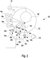
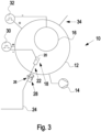
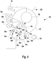
- FIG. 1 - 4 Each shows a plasma coating device 10 with a vacuum chamber 12, which can also be referred to as a process chamber or treatment chamber.
- the vacuum chamber 12 is evacuated by a fine vacuum pump 14.
- a substrate 16 to be coated is arranged in the vacuum chamber 12 of each embodiment.
- the substrate 16 can be one or more workpieces or other objects to be coated, which are fed into the vacuum chamber 12 and removed from the vacuum chamber 12 after coating has been completed.
- sputter source 18 In the embodiments according to the Fig. 1 and 3 In the vacuum chamber 12, exactly one sputter source 18 is arranged, while in the embodiments of the Fig. 2 and 4 Several, namely three, sputter sources 18a, 18b, 18c are provided. Each sputter source 18, 18a, 18b, 18c is designed as a hollow cathode, the circumferential surface of which forms a target 20.
- the target 20 is made of a solid material, preferably a metal.
- a carrier gas source 22, 22a, 22b, 22c, associated with the respective sputter source opens into the base of each sputter source 18, 18a, 18b, 18c, and is fed with carrier gas in the form of a noble gas, such as argon, from a supply line 24.
- a noble gas such as argon
- the supply line 24 is divided into corresponding supply branches 24a, 24b, 24c, wherein each of the supply branches 24a, 24b, 24c supplies exactly one corresponding carrier gas source 22a, 22b, 22c.
- the embodiments according to the Fig. 1 and 3 are in each supply line 24 and in the embodiments according to the Fig. 2 and 4 in each supply branch 24a, 24b, 24c two switchable valves 26, 28 or 26a, 28a; 26b, 28b; 26c, 28c are connected in parallel to each other in order to modulate the carrier gas supply to the respective Carrier gas source 22, 22a, 22b, 22c.
- valves can be shut-off valves or proportional valves.
- the number of valves per supply line or per supply branch is merely exemplary. Instead, only one valve per supply line is also possible in the Fig. 1 and 3 or per feed branch in the Fig. 2 and 4 conceivable, e.g. as a proportional valve.
- Each sputter source or target is configured as a cathode and connected to the negative terminal of a corresponding voltage supply source 30, or 30a, 30b, 30c.
- the positive terminal of the respective voltage supply source 30, 30a, 30b, 30c is connected to the housing of the vacuum chamber 12.
- the target is also connected to the negative terminal of another voltage supply source 32, whose positive terminal is connected to the vacuum chamber 12.
- the substrate 16 also forms a cathode, while the housing or the housing wall of the vacuum chamber 12 forms an anode.
- the examples of the Fig. 3 and 4 differ from those in the Fig. 1 and 2 each by an additional connection of a reactive gas source 34 to the vacuum chamber 12.
- Fig. 5 The solid line corresponds to the modulated course of the carrier gas flow from the carrier gas source 22 in the Fig. 1 and 3 or the carrier gas source 22a in the Fig. 2 and 4
- the dashed curve corresponds to the resulting curve of the modulated carrier gas flow of the carrier gas source 22b in the Fig. 2 and 4 .
- the dotted line in Fig. 5 the resulting course of the modulated carrier gas flow of the carrier gas source 22c in the Fig. 2 and 4 From Fig. 5 it is evident that Alternating switching of the valves 26a, 28a; 26b, 28b; 26c, 28c results in a pulsed flow of the supplied carrier gas flow into the vacuum chamber.
Landscapes
- Chemical & Material Sciences (AREA)
- Engineering & Computer Science (AREA)
- Chemical Kinetics & Catalysis (AREA)
- Materials Engineering (AREA)
- Mechanical Engineering (AREA)
- Metallurgy (AREA)
- Organic Chemistry (AREA)
- Physics & Mathematics (AREA)
- Plasma & Fusion (AREA)
- Analytical Chemistry (AREA)
- Physical Vapour Deposition (AREA)
Applications Claiming Priority (1)
| Application Number | Priority Date | Filing Date | Title |
|---|---|---|---|
| DE102023124377.2A DE102023124377A1 (de) | 2023-09-11 | 2023-09-11 | Verfahren zur Oberflächenbeschichtung nach dem Sputterprinzip |
Publications (2)
| Publication Number | Publication Date |
|---|---|
| EP4524282A2 true EP4524282A2 (fr) | 2025-03-19 |
| EP4524282A3 EP4524282A3 (fr) | 2025-06-11 |
Family
ID=92208911
Family Applications (1)
| Application Number | Title | Priority Date | Filing Date |
|---|---|---|---|
| EP24192386.1A Pending EP4524282A3 (fr) | 2023-09-11 | 2024-08-01 | Procédé de revêtement de surface par pulvérisation cathodique |
Country Status (3)
| Country | Link |
|---|---|
| US (1) | US20250084526A1 (fr) |
| EP (1) | EP4524282A3 (fr) |
| DE (1) | DE102023124377A1 (fr) |
Families Citing this family (1)
| Publication number | Priority date | Publication date | Assignee | Title |
|---|---|---|---|---|
| EP4471821A1 (fr) * | 2023-06-02 | 2024-12-04 | Melec Gmbh | Procédé de pulvérisation magnétron |
Citations (2)
| Publication number | Priority date | Publication date | Assignee | Title |
|---|---|---|---|---|
| DE4210125C2 (de) | 1992-03-27 | 1996-02-01 | Fraunhofer Ges Forschung | Vorrichtung zum Gasflußsputtern |
| EP1038045B1 (fr) | 1997-12-09 | 2013-11-13 | CemeCon AG | Procede de pulverisation cathodique magnetiquement renforcee |
Family Cites Families (8)
| Publication number | Priority date | Publication date | Assignee | Title |
|---|---|---|---|---|
| DE3809734C1 (fr) * | 1988-03-23 | 1989-05-03 | Helmut Prof. Dr. 7805 Boetzingen De Haberland | |
| JPH01312851A (ja) * | 1988-06-10 | 1989-12-18 | Fujitsu Ltd | 半導体装置の製造方法 |
| DE4441206C2 (de) * | 1994-11-19 | 1996-09-26 | Leybold Ag | Einrichtung für die Unterdrückung von Überschlägen in Kathoden-Zerstäubungseinrichtungen |
| US6458251B1 (en) * | 1999-11-16 | 2002-10-01 | Applied Materials, Inc. | Pressure modulation method to obtain improved step coverage of seed layer |
| US7381661B2 (en) * | 2002-10-15 | 2008-06-03 | Oc Oerlikon Balzers Ag | Method for the production of a substrate with a magnetron sputter coating and unit for the same |
| JP6239346B2 (ja) * | 2013-02-28 | 2017-11-29 | 株式会社アヤボ | パルススパッタ装置 |
| DE102013210155A1 (de) * | 2013-05-31 | 2014-12-04 | Fraunhofer-Gesellschaft zur Förderung der angewandten Forschung e.V. | Verfahren zum Abscheiden einer transparenten, elektrisch leitfähigen Metalloxidschicht |
| US9184029B2 (en) * | 2013-09-03 | 2015-11-10 | Lam Research Corporation | System, method and apparatus for coordinating pressure pulses and RF modulation in a small volume confined process reactor |
-
2023
- 2023-09-11 DE DE102023124377.2A patent/DE102023124377A1/de active Pending
-
2024
- 2024-08-01 EP EP24192386.1A patent/EP4524282A3/fr active Pending
- 2024-08-26 US US18/815,233 patent/US20250084526A1/en active Pending
Patent Citations (2)
| Publication number | Priority date | Publication date | Assignee | Title |
|---|---|---|---|---|
| DE4210125C2 (de) | 1992-03-27 | 1996-02-01 | Fraunhofer Ges Forschung | Vorrichtung zum Gasflußsputtern |
| EP1038045B1 (fr) | 1997-12-09 | 2013-11-13 | CemeCon AG | Procede de pulverisation cathodique magnetiquement renforcee |
Also Published As
| Publication number | Publication date |
|---|---|
| DE102023124377A1 (de) | 2025-03-13 |
| US20250084526A1 (en) | 2025-03-13 |
| EP4524282A3 (fr) | 2025-06-11 |
Similar Documents
| Publication | Publication Date | Title |
|---|---|---|
| EP0755461B1 (fr) | Procede et dispositif de revetement par evaporation sous vide par voie ionique | |
| EP0275018B1 (fr) | Procédé et appareil pour le revêtement de pièces conductrices par une décharge à arc | |
| DE69801106T2 (de) | Verfahren und vorrichtung zur niederdruckzerstäubung | |
| EP2236641B1 (fr) | Procédé de traitement préalable de substrats pour le procédé de PVD | |
| DE2307649B2 (de) | Anordnung zum Aufstäuben verschiedener Materialien auf einem Substrat | |
| DE3821207A1 (de) | Anordnung zum beschichten eines substrats mit dielektrika | |
| DE3614384A1 (de) | Verfahren zur beschichtung von substraten in einer vakuumkammer | |
| EP0529259A1 (fr) | Appareil pour le traitement de substrats | |
| EP2585622B1 (fr) | Source d'évaporation par arc présentant un champ électrique défini | |
| EP0803587A1 (fr) | Procédé et appareillage de dépÔt par pulvérisation cathodique | |
| EP2529386A1 (fr) | Dispositif de revêtement comprenant une source de puissance hipims (pulvérisation à magnétron pulsé à haute puissance) | |
| DE102011117994A1 (de) | HIPIMS-Schichten | |
| EP4524282A2 (fr) | Procédé de revêtement de surface par pulvérisation cathodique | |
| EP2439763B1 (fr) | Dispositif de magnétron et procédé de fonctionnement pulsé d'un dispositif à magnétron | |
| DE102016116762B4 (de) | Verfahren zum Abscheiden einer Schicht mittels einer Magnetronsputtereinrichtung | |
| WO2014008989A1 (fr) | Procédé de revêtement par impulsion haute puissance | |
| WO2022058193A1 (fr) | Appareil de revêtement et procédé de revêtement ayant des impulsions divisées | |
| DE102008022145B4 (de) | Vorrichtung und Verfahren zum Hochleistungs-Puls-Gasfluß-Sputtern | |
| DE10051508A1 (de) | Verfahren und Einrichtung zur Reduzierung Zündspannung von Leistungspulsen gepulst betriebener Plasmen | |
| DE2624005C2 (de) | Verfahren und Vorrichtung zum Aufbringen von dünnen Schichten auf ein Substrat nach dem "Ion-plating"-Verfahren. | |
| DE102015104433B3 (de) | Verfahren zum Betreiben einer Kaltkathoden-Elektronenstrahlquelle | |
| DE102014110835B4 (de) | Vorrichtung zum Bedampfen eines Substrates innerhalb einer Vakuumkammer | |
| EP3665315B1 (fr) | Dispositif de revêtement de surfaces de substrats par décharge de type arc électrique | |
| EP1473382A1 (fr) | Procédé et dispositif de déposition d'une couche activée par plasma par pulvérisation magnétron | |
| DD232513A1 (de) | Verdampfer fuer plasmagegestuetzte vakuum-beschichtungsverfahren |
Legal Events
| Date | Code | Title | Description |
|---|---|---|---|
| PUAI | Public reference made under article 153(3) epc to a published international application that has entered the european phase |
Free format text: ORIGINAL CODE: 0009012 |
|
| STAA | Information on the status of an ep patent application or granted ep patent |
Free format text: STATUS: THE APPLICATION HAS BEEN PUBLISHED |
|
| AK | Designated contracting states |
Kind code of ref document: A2 Designated state(s): AL AT BE BG CH CY CZ DE DK EE ES FI FR GB GR HR HU IE IS IT LI LT LU LV MC ME MK MT NL NO PL PT RO RS SE SI SK SM TR |
|
| PUAL | Search report despatched |
Free format text: ORIGINAL CODE: 0009013 |
|
| AK | Designated contracting states |
Kind code of ref document: A3 Designated state(s): AL AT BE BG CH CY CZ DE DK EE ES FI FR GB GR HR HU IE IS IT LI LT LU LV MC ME MK MT NL NO PL PT RO RS SE SI SK SM TR |
|
| RIC1 | Information provided on ipc code assigned before grant |
Ipc: C23C 14/22 20060101ALI20250506BHEP Ipc: H01J 37/32 20060101ALI20250506BHEP Ipc: H01J 37/34 20060101ALI20250506BHEP Ipc: C23C 14/35 20060101ALI20250506BHEP Ipc: C23C 14/34 20060101ALI20250506BHEP Ipc: C23C 14/00 20060101AFI20250506BHEP |
|
| STAA | Information on the status of an ep patent application or granted ep patent |
Free format text: STATUS: REQUEST FOR EXAMINATION WAS MADE |
|
| 17P | Request for examination filed |
Effective date: 20251205 |