EP4524943A1 - Circuit de commande et méthode de commande d'un pixel - Google Patents
Circuit de commande et méthode de commande d'un pixel Download PDFInfo
- Publication number
- EP4524943A1 EP4524943A1 EP23197615.0A EP23197615A EP4524943A1 EP 4524943 A1 EP4524943 A1 EP 4524943A1 EP 23197615 A EP23197615 A EP 23197615A EP 4524943 A1 EP4524943 A1 EP 4524943A1
- Authority
- EP
- European Patent Office
- Prior art keywords
- terminal
- type transistor
- drain terminal
- pixel
- driving circuit
- Prior art date
- Legal status (The legal status is an assumption and is not a legal conclusion. Google has not performed a legal analysis and makes no representation as to the accuracy of the status listed.)
- Pending
Links
Images







Classifications
-
- G—PHYSICS
- G09—EDUCATION; CRYPTOGRAPHY; DISPLAY; ADVERTISING; SEALS
- G09G—ARRANGEMENTS OR CIRCUITS FOR CONTROL OF INDICATING DEVICES USING STATIC MEANS TO PRESENT VARIABLE INFORMATION
- G09G3/00—Control arrangements or circuits, of interest only in connection with visual indicators other than cathode-ray tubes
- G09G3/20—Control arrangements or circuits, of interest only in connection with visual indicators other than cathode-ray tubes for presentation of an assembly of a number of characters, e.g. a page, by composing the assembly by combination of individual elements arranged in a matrix no fixed position being assigned to or needed to be assigned to the individual characters or partial characters
- G09G3/22—Control arrangements or circuits, of interest only in connection with visual indicators other than cathode-ray tubes for presentation of an assembly of a number of characters, e.g. a page, by composing the assembly by combination of individual elements arranged in a matrix no fixed position being assigned to or needed to be assigned to the individual characters or partial characters using controlled light sources
- G09G3/30—Control arrangements or circuits, of interest only in connection with visual indicators other than cathode-ray tubes for presentation of an assembly of a number of characters, e.g. a page, by composing the assembly by combination of individual elements arranged in a matrix no fixed position being assigned to or needed to be assigned to the individual characters or partial characters using controlled light sources using electroluminescent panels
- G09G3/32—Control arrangements or circuits, of interest only in connection with visual indicators other than cathode-ray tubes for presentation of an assembly of a number of characters, e.g. a page, by composing the assembly by combination of individual elements arranged in a matrix no fixed position being assigned to or needed to be assigned to the individual characters or partial characters using controlled light sources using electroluminescent panels semiconductive, e.g. using light-emitting diodes [LED]
-
- G—PHYSICS
- G09—EDUCATION; CRYPTOGRAPHY; DISPLAY; ADVERTISING; SEALS
- G09G—ARRANGEMENTS OR CIRCUITS FOR CONTROL OF INDICATING DEVICES USING STATIC MEANS TO PRESENT VARIABLE INFORMATION
- G09G2300/00—Aspects of the constitution of display devices
- G09G2300/04—Structural and physical details of display devices
- G09G2300/0421—Structural details of the set of electrodes
- G09G2300/0426—Layout of electrodes and connections
-
- G—PHYSICS
- G09—EDUCATION; CRYPTOGRAPHY; DISPLAY; ADVERTISING; SEALS
- G09G—ARRANGEMENTS OR CIRCUITS FOR CONTROL OF INDICATING DEVICES USING STATIC MEANS TO PRESENT VARIABLE INFORMATION
- G09G2300/00—Aspects of the constitution of display devices
- G09G2300/08—Active matrix structure, i.e. with use of active elements, inclusive of non-linear two terminal elements, in the pixels together with light emitting or modulating elements
- G09G2300/0809—Several active elements per pixel in active matrix panels
- G09G2300/0814—Several active elements per pixel in active matrix panels used for selection purposes, e.g. logical AND for partial update
-
- G—PHYSICS
- G09—EDUCATION; CRYPTOGRAPHY; DISPLAY; ADVERTISING; SEALS
- G09G—ARRANGEMENTS OR CIRCUITS FOR CONTROL OF INDICATING DEVICES USING STATIC MEANS TO PRESENT VARIABLE INFORMATION
- G09G2310/00—Command of the display device
- G09G2310/02—Addressing, scanning or driving the display screen or processing steps related thereto
- G09G2310/0264—Details of driving circuits
- G09G2310/0275—Details of drivers for data electrodes, other than drivers for liquid crystal, plasma or OLED displays, not related to handling digital grey scale data or to communication of data to the pixels by means of a current
-
- G—PHYSICS
- G09—EDUCATION; CRYPTOGRAPHY; DISPLAY; ADVERTISING; SEALS
- G09G—ARRANGEMENTS OR CIRCUITS FOR CONTROL OF INDICATING DEVICES USING STATIC MEANS TO PRESENT VARIABLE INFORMATION
- G09G3/00—Control arrangements or circuits, of interest only in connection with visual indicators other than cathode-ray tubes
- G09G3/20—Control arrangements or circuits, of interest only in connection with visual indicators other than cathode-ray tubes for presentation of an assembly of a number of characters, e.g. a page, by composing the assembly by combination of individual elements arranged in a matrix no fixed position being assigned to or needed to be assigned to the individual characters or partial characters
- G09G3/22—Control arrangements or circuits, of interest only in connection with visual indicators other than cathode-ray tubes for presentation of an assembly of a number of characters, e.g. a page, by composing the assembly by combination of individual elements arranged in a matrix no fixed position being assigned to or needed to be assigned to the individual characters or partial characters using controlled light sources
- G09G3/30—Control arrangements or circuits, of interest only in connection with visual indicators other than cathode-ray tubes for presentation of an assembly of a number of characters, e.g. a page, by composing the assembly by combination of individual elements arranged in a matrix no fixed position being assigned to or needed to be assigned to the individual characters or partial characters using controlled light sources using electroluminescent panels
- G09G3/32—Control arrangements or circuits, of interest only in connection with visual indicators other than cathode-ray tubes for presentation of an assembly of a number of characters, e.g. a page, by composing the assembly by combination of individual elements arranged in a matrix no fixed position being assigned to or needed to be assigned to the individual characters or partial characters using controlled light sources using electroluminescent panels semiconductive, e.g. using light-emitting diodes [LED]
- G09G3/3208—Control arrangements or circuits, of interest only in connection with visual indicators other than cathode-ray tubes for presentation of an assembly of a number of characters, e.g. a page, by composing the assembly by combination of individual elements arranged in a matrix no fixed position being assigned to or needed to be assigned to the individual characters or partial characters using controlled light sources using electroluminescent panels semiconductive, e.g. using light-emitting diodes [LED] organic, e.g. using organic light-emitting diodes [OLED]
- G09G3/3225—Control arrangements or circuits, of interest only in connection with visual indicators other than cathode-ray tubes for presentation of an assembly of a number of characters, e.g. a page, by composing the assembly by combination of individual elements arranged in a matrix no fixed position being assigned to or needed to be assigned to the individual characters or partial characters using controlled light sources using electroluminescent panels semiconductive, e.g. using light-emitting diodes [LED] organic, e.g. using organic light-emitting diodes [OLED] using an active matrix
- G09G3/3233—Control arrangements or circuits, of interest only in connection with visual indicators other than cathode-ray tubes for presentation of an assembly of a number of characters, e.g. a page, by composing the assembly by combination of individual elements arranged in a matrix no fixed position being assigned to or needed to be assigned to the individual characters or partial characters using controlled light sources using electroluminescent panels semiconductive, e.g. using light-emitting diodes [LED] organic, e.g. using organic light-emitting diodes [OLED] using an active matrix with pixel circuitry controlling the current through the light-emitting element
Definitions
- the invention relates to pixel driving circuitry, especially to display drivers for driving pixels of a display.
- LEDs light-emitting diodes
- TFT Thin Film Transistor
- OLED Organic Light-Emitting Diode
- new display technologies such as micro LEDs (uLED) are more amenable to common-anode configuration in view of process technology.
- the document EP 2 642 476 B1 discloses separate pixel driving circuits for driving OLED pixels with common-anode and common-cathode configurations.
- the separate driver circuitry may limit the flexibility to select the display configurations based on a target application.
- designing a completely new driver circuitry tailor-made for the available or selected display configuration may be time consuming and cost-intensive.
- an object of the invention is to provide a driving circuit and a method to facilitate a unified pixel driver that can drive either a common-cathode or common-anode configured LED display, in order to address the above-mentioned limitations.
- a driving circuit for driving a pixel of a display.
- the driving circuit comprises at least one pMOS type transistor comprising a gate terminal, a source terminal, and a drain terminal; at least one nMOS type transistor comprising a gate terminal, a source terminal, and a drain terminal; and a metal base comprising an output terminal.
- the metal base is configured to connect the drain terminal of the at least one pMOS type transistor or the drain terminal of the at least one nMOS type transistor to the output terminal to output a driving signal for driving the pixel.
- the invention solves the problem of driving LED displays with common-anode or common-cathode configurations using a single, unified CMOS ASIC driver design, which advantageously facilitates a far more flexibility in selecting the display configuration based on the target application.
- the metal base may be modified or fixed, e.g., for the drain to output terminal connection based on the selected or available display configuration, at the CMOS processing fabrication, which may allow switching between the two configurations with minimal cost.
- the driving circuit further comprises an input node configured to connect the gate terminal of the at least one pMOS type transistor and the gate terminal of the at least one nMOS type transistor, and an input terminal connected to the input node.
- the input terminal is configured to input an input signal to the input node to drive the at least one pMOS type transistor or the at least one nMOS type transistor.
- the input signal may be of polarity suitable, e.g., for the nMOS type transistor and the common-anode configuration, and for the pMOS type transistor and the common-cathode configuration.
- the driving circuit further comprises a switching arrangement configured to connect the input terminal to the input node in a switchable manner.
- the switching arrangement comprises or is a high voltage switch, preferably a high voltage transistor, more preferably a high voltage nMOS transistor.
- the high voltage transistor switch may be advantageous when the drive transistors operate in saturation or current mode.
- the high voltage transistor switch may help to transfer both low and high, e.g., 0 and 1, input values perfectly to the gate of the drive transistors.
- the use of a single transistor may reduce one transistor from the commonly used transmission gate data switches.
- the source terminal of the at least one pMOS type transistor is connected to a reference potential and the source terminal of the at least one nMOS type transistor is connected to a ground potential.
- a fast and reliable switching between the drive transistors can be achieved based on the selected display configuration, especially during the display driver manufacturing process.
- the pixel corresponds to a pixel of a common-anode display, and the source terminal and the drain terminal of the at least one pMOS type transistor are interconnected (i.e., the excluded or unused transistor).
- the pixel corresponds to a pixel of a common-cathode display, and the source terminal and the drain terminal of the at least one nMOS type transistor are interconnected (i.e., the excluded or unused transistor).
- the interconnection between the source and drain terminals of an unused transistor may increase the implicit storage capacitance, thereby improving the display performance. Furthermore, such an interconnection may prevent an open drain connection of the unused transistor.
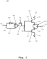
- the driving circuit comprises a further metal base and an inverter
- the further metal base is configured to connect the input terminal to the input node or to connect the input terminal to the input node via the inverter.
- the input signal may be of polarity suitable for the nMOS type transistor
- the further metal base may connect the input terminal to the input node for the common-anode configuration.
- the further metal base may connect the input terminal to the input node via the inverter in order to correct the polarity for the pMOS type transistor.
- the metal base comprises a first stacked via arranged at a metal layer corresponding to the drain terminal of the at least one pMOS type transistor, a second stacked via arranged at a metal layer corresponding to the drain terminal of the at least one nMOS type transistor, and a single metal layer connecting the first stacked via or the second stacked via to the output terminal.
- the metal layers corresponding to the drain terminals may involve different metal layers within the area of the metal base.
- the respective stacked via or via-stacks may advantageously bring up the different metal layers to the metal layer of the output terminal, preferably at the top metal layer.
- This may facilitate a top-level design where only one metal network connects the correct data lines to the common connection of the LEDs.
- the use of only one metal network may further reduce metal congestion across the display, parasitics, power consumption, and area, and may improve the speed of operation.
- a display system comprises a common-anode display comprising a plurality of pixels; each of the plurality of pixels comprises at least one light emitting device, and a plurality of driving circuits according to the first aspect of the invention.
- each of the output terminal of the plurality of driving circuits being connected to the at least one light emitting device of the respective plurality of pixels of the common-anode display and further to the drain terminal of the respective nMOS type transistor, especially via the metal base.
- a further display system comprises a common-cathode display comprising a plurality of pixels; each of the plurality of pixels comprises at least one light emitting device, and a plurality of driving circuits according to the first aspect of the invention.
- each of the output terminal of the plurality of driving circuits being connected to the at least one light emitting device of the respective plurality of pixels of the common-cathode display and further to the drain terminal of the respective pMOS type transistor, especially via the metal base.
- the method further comprises the steps of connecting the gate terminal of the at least one pMOS type transistor and the gate terminal of the at least one nMOS type transistor to an input node; and inputting or connecting an input signal to the input node via an input terminal connected to the input node to drive the at least one pMOS type transistor or the at least one nMOS type transistor.
- the method further comprises the steps of arranging a first stacked via at a metal layer corresponding to the drain terminal of the at least one pMOS type transistor; arranging a second stacked via at a metal layer corresponding to the drain terminal of the at least one nMOS type transistor; and connecting the first stacked via or the second stacked via to the output terminal using a single metal layer.
- the display system according to the second aspect, the display system according to the third aspect, and the method according to the fourth aspect correspond to the driving circuit according to the first aspect and its implementation forms. Accordingly, the display system according to the second aspect, the display system according to the third aspect, and the method according to the fourth aspect may have corresponding implementation forms.
- the driving circuit 100 may comprise a metal base or a metal fix 130, where the drain terminal 113 of the pMOS transistor 110 and the drain terminal 123 of the nMOS transistor 120 may be arranged on or in relation to the metal base 130.
- the metal base 130 may comprise an output terminal 131 to be connected to a pixel, e.g., an LED, of a display, especially to drive the pixel.
- the driving circuit 100 may comprise a switch 160 that may connect the input terminal 150 to the input node 140 in a switching manner, e.g., via a switch control signal or switch signal 161.
- the switch 160 may comprise one or more transistors, e.g., an nMOS transistor as illustrated herein.
- the switch 160 may comprise or be a high-voltage transistor, e.g., a high-voltage nMOS transistor.
- the source terminal 112 of the pMOS transistor 110 may be connected to a reference potential or supply 170, and the source terminal 122 of the nMOS transistor 120 may be connected to a ground potential or ground 180.
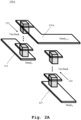
- the metal base 130A may be formed to drive a pixel of a common-cathode display, i.e., the pixel should be driven by the pMOS transistor 110.
- the metal line corresponding to the drain terminal 113 of the pMOS transistor 110 and the metal line corresponding to the drain terminal 123 of the nMOS transistor 120 may correspond to a metal layer Metal X .
- a first stacked via 133 may be arranged at the metal line of the drain terminal 113 at the Metal X layer, and a second stacked via 134 may be arranged at the metal line of the drain terminal 123 at the Metal X layer, especially to raise the Metal X layer by a number of Y layers to arrive at a top level layer Metal X+Y .
- the output terminal 131 may be arranged at the Metal X+Y layer.
- a single metal layer 135A may be realized to connect the first stacked via 133 to the output terminal 131, i.e., to connect the drain terminal 113 of the pMOS transistor 110 to the output terminal 131 at the Metal X+Y layer.
- the metal base 130B may be formed to drive a pixel of a common-anode display, i.e., the pixel should be driven by the nMOS transistor 120.
- the metal line corresponding to the drain terminal 113 of the pMOS transistor 110 and the metal line corresponding to the drain terminal 123 of the nMOS transistor 120 may correspond to a metal layer Metal X .
- a first stacked via 133 may be arranged at the metal line of the drain terminal 113 at the Metal X layer, and a second stacked via 134 may be arranged at the metal line of the drain terminal 123 at the Metal X layer, especially to raise the Metal X layer by a number of Y layers to arrive at a top level layer Metal X+Y .
- the output terminal 131 may be arranged at the Metal X+Y layer.
- a single metal layer 135B may be realized to connect the second stacked via 134 to the output terminal 131, i.e., to connect the drain terminal 123 of the nMOS transistor 120 to the output terminal 131 at the Metal X+Y layer.
- the metal base 130A, 130B may initially comprise the first stacked via 133 arranged at the drain terminal 113 of the pMOS transistor 110 at the Metal X layer to raise the terminal connection to the Metal X+Y layer, the second stacked via 134 arranged at the drain terminal 123 of the nMOS transistor 120 at the Metal X layer to raise the terminal connection to the Metal X+Y layer, and the output terminal 131 arranged at the Metal X+Y layer.
- the respective single metal layer or line 135A, 135B may be formed, i.e., the single metal layer 135A for the common-cathode display or the single metal layer 135B for the common-anode display.
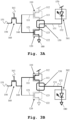
- a first exemplary pixel connection scheme especially to drive a pixel of a common-anode display, is illustrated.
- an LED 301 of a pixel of the common-anode display may be connected to the supply 170, i.e., the common-anode rail, and be driven by an nMOS transistor.
- the driving circuit 100 may be arranged such that the drain terminal 123 of the nMOS transistor 120 may be connected to the output terminal 131 connecting the LED pin, especially to drive the LED 301 by providing the driving signal 132.
- connection between the drain terminal 123 of the nMOS transistor 120 and the output terminal 131 may be realized via the metal base 130B, especially via the single metal layer 135B, where the drain terminal 113 of the pMOS transistor 110 being disconnected, thereby excluding the pMOS transistor 110 (as shown in gray).
- a second exemplary pixel connection scheme especially to drive a pixel of a common-cathode display, is illustrated.
- an LED 302 of a pixel of the common-cathode display may be connected to the ground 170, i.e., the common-cathode ground, and be driven by a pMOS transistor.
- the driving circuit 100 may be arranged such that the drain terminal 113 of the pMOS transistor 110 may be connected to the output terminal 131 connecting the LED pin, especially to drive the LED 302 by providing the driving signal 132.
- connection between the drain terminal 113 of the pMOS transistor 110 and the output terminal 131 may be realized via the metal base 130A, especially via the single metal layer 135A, where the drain terminal 123 of the nMOS transistor 120 being disconnected, thereby excluding the nMOS transistor 120 (as shown in gray).
- a third exemplary pixel connection scheme especially to drive a pixel of a common-anode display, is illustrated.
- the LED 301 of a pixel of the common-anode display may be connected to the supply 170 and be driven by an nMOS transistor.
- connection scheme differs from the connection scheme of Fig. 3A in that the source terminal 112 and the drain terminal 113 of the pMOS transistor 110, i.e., of the excluded pMOS transistor 110 shown in grey, may be connected together, and to the supply 170 via a first interconnection 401.
- connection between the drain terminal 123 of the nMOS transistor 120 and the output terminal 131 may be realized via the metal base 130B, especially via the single metal layer 135B.
- the source terminal 112 of the pMOS transistor 110 may be raised to Metal X+Y layer, e.g., by means of a further stacked via.
- the interconnection 401 may be realized, e.g., by means of a further metal line connecting the stacked vias, at the Metal X+Y layer to interconnect the source terminal 112 and the drain terminal 113 of the pMOS transistor 110.
- a fourth exemplary pixel connection scheme especially to drive a pixel of a common-cathode display, is illustrated.
- the LED 302 of a pixel of the common-cathode display may be connected to the ground 180 and be driven by a pMOS transistor.
- connection scheme differs from the connection scheme of Fig. 3B in that the source terminal 122 and the drain terminal 123 of the nMOS transistor 120, i.e., of the excluded nMOS transistor 120 shown in grey, may be connected together, and to the ground 180 via a second interconnection 402.
- connection between the drain terminal 113 of the pMOS transistor 110 and the output terminal 131 may be realized via the metal base 130A, especially via the single metal layer 135A.
- the source terminal 122 of the nMOS transistor 120 may be raised to Metal X+Y layer, e.g., by means of a further stacked via.
- the interconnection 402 may be realized, e.g., by means of a further metal line connecting the stacked vias, at the Metal X+Y layer to interconnect the source terminal 122 and the drain terminal 123 of the nMOS transistor 120.
- the first path connected to the further metal base 501 may be raised to the Metal X+Y layer, e.g., by means of a stacked via
- the second path 503 connected to the further metal base 501, especially the connection to the second path 503 may be raised to the Metal X+Y layer.
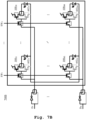
- a common data line D 1 -D m may be arranged per row connecting the input terminals 150 of the respective driving circuits 100 11 -100 mn , arranged in said row.
- a common switch line SW 1 -SW n may be arranged per column connecting the switches 160 of the respective driving circuits 100 11 -100 mn , arranged in said column.
- a common data line D 1 -D m may be arranged per row connecting the input terminals 150 of the respective driving circuits 100 11 -100 mn , arranged in said row.
- a common switch line SW 1 -SW n may be arranged per column connecting the switches 160 of the respective driving circuits 100 11 -100 mn , arranged in said column.
- a second exemplary embodiment of the display system 700B according to the third aspect of the invention in a common-cathode configuration is illustrated.
- the display system 700B may differ from the display system 600B in that the display system 700B may additionally comprise the inverter arrangement of Fig. 5 , especially realized such that only one inverter arrangement may be implemented per row of the driving circuits 100 11 -100 mn .
- the respective driving circuit 100 11 -100 mn may be replaced with the driving circuit 500 such that one further metal base 501 and one inverter arrangement comprising the inverter 502 and the direct path 503 may be arranged per driving circuit 100 11 -100 mn .
- the common data line D 1 -D m per row may be connected to the respective input terminals 150 of the inverter arrangements of the respective driving circuits arranged in said row.
- the metal base 501 may connect the direct path 503 to the input terminals 150.
- a third exemplary embodiment of the display system 800B according to the third aspect of the invention in a common-cathode configuration is illustrated.
- the display system 800B may differ from the display system 600B in that the display system 800B may additionally comprise the inverter arrangement of Fig. 5 , especially realized such that each of the driving circuits 100 11 -100 mn , may comprise the inverter arrangement.
Landscapes
- Engineering & Computer Science (AREA)
- Physics & Mathematics (AREA)
- Computer Hardware Design (AREA)
- General Physics & Mathematics (AREA)
- Theoretical Computer Science (AREA)
- Control Of Indicators Other Than Cathode Ray Tubes (AREA)
- Devices For Indicating Variable Information By Combining Individual Elements (AREA)
Priority Applications (3)
| Application Number | Priority Date | Filing Date | Title |
|---|---|---|---|
| EP23197615.0A EP4524943A1 (fr) | 2023-09-15 | 2023-09-15 | Circuit de commande et méthode de commande d'un pixel |
| CN202480042299.9A CN121420349A (zh) | 2023-09-15 | 2024-07-17 | 用于驱动像素的驱动电路和方法 |
| PCT/EP2024/070233 WO2025056223A1 (fr) | 2023-09-15 | 2024-07-17 | Circuit d'attaque et procédé d'excitation de pixel |
Applications Claiming Priority (1)
| Application Number | Priority Date | Filing Date | Title |
|---|---|---|---|
| EP23197615.0A EP4524943A1 (fr) | 2023-09-15 | 2023-09-15 | Circuit de commande et méthode de commande d'un pixel |
Publications (1)
| Publication Number | Publication Date |
|---|---|
| EP4524943A1 true EP4524943A1 (fr) | 2025-03-19 |
Family
ID=88092902
Family Applications (1)
| Application Number | Title | Priority Date | Filing Date |
|---|---|---|---|
| EP23197615.0A Pending EP4524943A1 (fr) | 2023-09-15 | 2023-09-15 | Circuit de commande et méthode de commande d'un pixel |
Country Status (3)
| Country | Link |
|---|---|
| EP (1) | EP4524943A1 (fr) |
| CN (1) | CN121420349A (fr) |
| WO (1) | WO2025056223A1 (fr) |
Citations (10)
| Publication number | Priority date | Publication date | Assignee | Title |
|---|---|---|---|---|
| US20030080687A1 (en) * | 2001-10-26 | 2003-05-01 | Shinichi Fukuzako | Drive circuit |
| US20030117388A1 (en) * | 2001-12-07 | 2003-06-26 | Jun Koyama | Display device and electric equipment using the same |
| US20050007316A1 (en) * | 2003-05-15 | 2005-01-13 | Hajime Akimoto | Image display device |
| US20060028407A1 (en) * | 2004-08-06 | 2006-02-09 | Chen-Jean Chou | Light emitting device display circuit and drive method thereof |
| US20060238475A1 (en) * | 2003-12-29 | 2006-10-26 | Lg.Philips Lcd Co. Ltd. | Organic electroluminescent display device and driving method thereof |
| US20070046611A1 (en) * | 2003-04-29 | 2007-03-01 | Cambridge Display Technology Limited | Pwm driver for a passive matrix display and corresponding method |
| EP2642476B1 (fr) | 2012-03-23 | 2015-01-14 | Samsung Display Co., Ltd. | Circuit de pixels, procédé de commande d'un circuit de pixels et dispositif d'affichage électroluminescent organique |
| US20170352314A1 (en) * | 2016-06-02 | 2017-12-07 | Joled Inc. | Display device |
| US20220344425A1 (en) * | 2021-02-20 | 2022-10-27 | Boe Technology Group Co., Ltd. | Display panel and display apparatus |
| CN116528630A (zh) * | 2023-06-15 | 2023-08-01 | 上海天马微电子有限公司 | 一种显示面板以及电子设备 |
-
2023
- 2023-09-15 EP EP23197615.0A patent/EP4524943A1/fr active Pending
-
2024
- 2024-07-17 CN CN202480042299.9A patent/CN121420349A/zh active Pending
- 2024-07-17 WO PCT/EP2024/070233 patent/WO2025056223A1/fr active Pending
Patent Citations (11)
| Publication number | Priority date | Publication date | Assignee | Title |
|---|---|---|---|---|
| US20030080687A1 (en) * | 2001-10-26 | 2003-05-01 | Shinichi Fukuzako | Drive circuit |
| US20030117388A1 (en) * | 2001-12-07 | 2003-06-26 | Jun Koyama | Display device and electric equipment using the same |
| US20070046611A1 (en) * | 2003-04-29 | 2007-03-01 | Cambridge Display Technology Limited | Pwm driver for a passive matrix display and corresponding method |
| US20050007316A1 (en) * | 2003-05-15 | 2005-01-13 | Hajime Akimoto | Image display device |
| US20060238475A1 (en) * | 2003-12-29 | 2006-10-26 | Lg.Philips Lcd Co. Ltd. | Organic electroluminescent display device and driving method thereof |
| US20060028407A1 (en) * | 2004-08-06 | 2006-02-09 | Chen-Jean Chou | Light emitting device display circuit and drive method thereof |
| EP2642476B1 (fr) | 2012-03-23 | 2015-01-14 | Samsung Display Co., Ltd. | Circuit de pixels, procédé de commande d'un circuit de pixels et dispositif d'affichage électroluminescent organique |
| US20170352314A1 (en) * | 2016-06-02 | 2017-12-07 | Joled Inc. | Display device |
| US20220344425A1 (en) * | 2021-02-20 | 2022-10-27 | Boe Technology Group Co., Ltd. | Display panel and display apparatus |
| CN116528630A (zh) * | 2023-06-15 | 2023-08-01 | 上海天马微电子有限公司 | 一种显示面板以及电子设备 |
| US20230413642A1 (en) * | 2023-06-15 | 2023-12-21 | Shanghai Tianma Micro-electronics Co., Ltd. | Display panel and electronic device |
Also Published As
| Publication number | Publication date |
|---|---|
| CN121420349A (zh) | 2026-01-27 |
| WO2025056223A1 (fr) | 2025-03-20 |
Similar Documents
| Publication | Publication Date | Title |
|---|---|---|
| CN108074531B (zh) | 电致发光显示器中的电压补偿电路 | |
| US9082344B2 (en) | Pixel circuit in flat panel display device and method for driving the same | |
| CN114220392B (zh) | 微型发光二极体显示面板及其画素驱动电路 | |
| KR100668270B1 (ko) | 전자 장치 및 전자 기기 | |
| JP4641896B2 (ja) | 発光表示装置,デマルチプレキシング回路およびその駆動方法 | |
| CN110136637B (zh) | 一种像素电路及其驱动方法、显示装置 | |
| KR20180089928A (ko) | 표시 장치 | |
| KR102861589B1 (ko) | 발광 표시 장치 | |
| US20080030439A1 (en) | Organic light emitting display device | |
| KR102748978B1 (ko) | 표시 장치 | |
| JP2012507038A (ja) | アクティブマトリクスoledディスプレイおよびその駆動回路 | |
| JP2010020154A (ja) | 発光表示装置およびその駆動方法 | |
| TW202226196A (zh) | 微發光二極體顯示裝置及其次畫素電路 | |
| CN111508431A (zh) | 像素驱动电路、方法以及显示装置 | |
| US12555525B2 (en) | Driver circuit for light emitting modules with combined active and passive matrix functionalities | |
| US8427403B2 (en) | Demultiplexer, display apparatus using the same, and display panel thereof | |
| CN101379543A (zh) | 无源矩阵显示驱动器 | |
| KR20110103453A (ko) | 유기 el 표시 장치 및 그 마더 기판, 및 그 검사 방법 | |
| CN101206830B (zh) | 内部像素回旋排列的主动式有机发光显示器 | |
| CN113539170B (zh) | 像素驱动电路及其驱动方法、显示基板、显示装置 | |
| WO2025056223A1 (fr) | Circuit d'attaque et procédé d'excitation de pixel | |
| EP3557949B1 (fr) | Dispositif électrique apte à réduire l'interférence lumineuse | |
| KR20080059010A (ko) | 유기 el 표시장치 및 그의 구동방법 | |
| US7208294B2 (en) | Display device and display panel driving method | |
| WO2024197556A1 (fr) | Substrat de réseau et appareil d'affichage |
Legal Events
| Date | Code | Title | Description |
|---|---|---|---|
| PUAI | Public reference made under article 153(3) epc to a published international application that has entered the european phase |
Free format text: ORIGINAL CODE: 0009012 |
|
| STAA | Information on the status of an ep patent application or granted ep patent |
Free format text: STATUS: THE APPLICATION HAS BEEN PUBLISHED |
|
| AK | Designated contracting states |
Kind code of ref document: A1 Designated state(s): AL AT BE BG CH CY CZ DE DK EE ES FI FR GB GR HR HU IE IS IT LI LT LU LV MC ME MK MT NL NO PL PT RO RS SE SI SK SM TR |
|
| STAA | Information on the status of an ep patent application or granted ep patent |
Free format text: STATUS: REQUEST FOR EXAMINATION WAS MADE |
|
| 17P | Request for examination filed |
Effective date: 20250409 |