EP4525031A1 - Fabrication de plaquettes semi-conductrices avec conversion de polyimide en graphène - Google Patents
Fabrication de plaquettes semi-conductrices avec conversion de polyimide en graphène Download PDFInfo
- Publication number
- EP4525031A1 EP4525031A1 EP24199255.1A EP24199255A EP4525031A1 EP 4525031 A1 EP4525031 A1 EP 4525031A1 EP 24199255 A EP24199255 A EP 24199255A EP 4525031 A1 EP4525031 A1 EP 4525031A1
- Authority
- EP
- European Patent Office
- Prior art keywords
- layer
- graphene
- dielectric layer
- opening
- polyimide
- Prior art date
- Legal status (The legal status is an assumption and is not a legal conclusion. Google has not performed a legal analysis and makes no representation as to the accuracy of the status listed.)
- Granted
Links
Images


Classifications
-
- H—ELECTRICITY
- H10—SEMICONDUCTOR DEVICES; ELECTRIC SOLID-STATE DEVICES NOT OTHERWISE PROVIDED FOR
- H10W—GENERIC PACKAGES, INTERCONNECTIONS, CONNECTORS OR OTHER CONSTRUCTIONAL DETAILS OF DEVICES COVERED BY CLASS H10
- H10W20/00—Interconnections in chips, wafers or substrates
- H10W20/40—Interconnections external to wafers or substrates, e.g. back-end-of-line [BEOL] metallisations or vias connecting to gate electrodes
- H10W20/41—Interconnections external to wafers or substrates, e.g. back-end-of-line [BEOL] metallisations or vias connecting to gate electrodes characterised by their conductive parts
- H10W20/42—Vias, e.g. via plugs
-
- H—ELECTRICITY
- H10—SEMICONDUCTOR DEVICES; ELECTRIC SOLID-STATE DEVICES NOT OTHERWISE PROVIDED FOR
- H10W—GENERIC PACKAGES, INTERCONNECTIONS, CONNECTORS OR OTHER CONSTRUCTIONAL DETAILS OF DEVICES COVERED BY CLASS H10
- H10W20/00—Interconnections in chips, wafers or substrates
- H10W20/01—Manufacture or treatment
- H10W20/031—Manufacture or treatment of conductive parts of the interconnections
- H10W20/056—Manufacture or treatment of conductive parts of the interconnections by filling conductive material into holes, grooves or trenches
-
- H—ELECTRICITY
- H10—SEMICONDUCTOR DEVICES; ELECTRIC SOLID-STATE DEVICES NOT OTHERWISE PROVIDED FOR
- H10W—GENERIC PACKAGES, INTERCONNECTIONS, CONNECTORS OR OTHER CONSTRUCTIONAL DETAILS OF DEVICES COVERED BY CLASS H10
- H10W20/00—Interconnections in chips, wafers or substrates
- H10W20/01—Manufacture or treatment
- H10W20/031—Manufacture or treatment of conductive parts of the interconnections
- H10W20/067—Manufacture or treatment of conductive parts of the interconnections by modifying the pattern of conductive parts
- H10W20/068—Manufacture or treatment of conductive parts of the interconnections by modifying the pattern of conductive parts by using a laser, e.g. laser cutting or laser direct writing
-
- H—ELECTRICITY
- H10—SEMICONDUCTOR DEVICES; ELECTRIC SOLID-STATE DEVICES NOT OTHERWISE PROVIDED FOR
- H10W—GENERIC PACKAGES, INTERCONNECTIONS, CONNECTORS OR OTHER CONSTRUCTIONAL DETAILS OF DEVICES COVERED BY CLASS H10
- H10W20/00—Interconnections in chips, wafers or substrates
- H10W20/01—Manufacture or treatment
- H10W20/071—Manufacture or treatment of dielectric parts thereof
- H10W20/081—Manufacture or treatment of dielectric parts thereof by forming openings in the dielectric parts
-
- H—ELECTRICITY
- H10—SEMICONDUCTOR DEVICES; ELECTRIC SOLID-STATE DEVICES NOT OTHERWISE PROVIDED FOR
- H10W—GENERIC PACKAGES, INTERCONNECTIONS, CONNECTORS OR OTHER CONSTRUCTIONAL DETAILS OF DEVICES COVERED BY CLASS H10
- H10W20/00—Interconnections in chips, wafers or substrates
- H10W20/01—Manufacture or treatment
- H10W20/071—Manufacture or treatment of dielectric parts thereof
- H10W20/081—Manufacture or treatment of dielectric parts thereof by forming openings in the dielectric parts
- H10W20/084—Manufacture or treatment of dielectric parts thereof by forming openings in the dielectric parts for dual-damascene structures
- H10W20/085—Manufacture or treatment of dielectric parts thereof by forming openings in the dielectric parts for dual-damascene structures involving intermediate temporary filling with material
-
- H—ELECTRICITY
- H10—SEMICONDUCTOR DEVICES; ELECTRIC SOLID-STATE DEVICES NOT OTHERWISE PROVIDED FOR
- H10W—GENERIC PACKAGES, INTERCONNECTIONS, CONNECTORS OR OTHER CONSTRUCTIONAL DETAILS OF DEVICES COVERED BY CLASS H10
- H10W20/00—Interconnections in chips, wafers or substrates
- H10W20/01—Manufacture or treatment
- H10W20/071—Manufacture or treatment of dielectric parts thereof
- H10W20/093—Manufacture or treatment of dielectric parts thereof by modifying materials of the dielectric parts
- H10W20/094—Manufacture or treatment of dielectric parts thereof by modifying materials of the dielectric parts by transforming insulators into conductors
-
- H—ELECTRICITY
- H10—SEMICONDUCTOR DEVICES; ELECTRIC SOLID-STATE DEVICES NOT OTHERWISE PROVIDED FOR
- H10W—GENERIC PACKAGES, INTERCONNECTIONS, CONNECTORS OR OTHER CONSTRUCTIONAL DETAILS OF DEVICES COVERED BY CLASS H10
- H10W20/00—Interconnections in chips, wafers or substrates
- H10W20/40—Interconnections external to wafers or substrates, e.g. back-end-of-line [BEOL] metallisations or vias connecting to gate electrodes
- H10W20/41—Interconnections external to wafers or substrates, e.g. back-end-of-line [BEOL] metallisations or vias connecting to gate electrodes characterised by their conductive parts
- H10W20/425—Barrier, adhesion or liner layers
-
- H—ELECTRICITY
- H10—SEMICONDUCTOR DEVICES; ELECTRIC SOLID-STATE DEVICES NOT OTHERWISE PROVIDED FOR
- H10W—GENERIC PACKAGES, INTERCONNECTIONS, CONNECTORS OR OTHER CONSTRUCTIONAL DETAILS OF DEVICES COVERED BY CLASS H10
- H10W20/00—Interconnections in chips, wafers or substrates
- H10W20/40—Interconnections external to wafers or substrates, e.g. back-end-of-line [BEOL] metallisations or vias connecting to gate electrodes
- H10W20/41—Interconnections external to wafers or substrates, e.g. back-end-of-line [BEOL] metallisations or vias connecting to gate electrodes characterised by their conductive parts
- H10W20/44—Conductive materials thereof
- H10W20/4462—Carbon or carbon-containing materials, e.g. graphene
Definitions
- the present disclosure is directed in general to the field of semiconductor devices.
- the present disclosure relates to inter-level interconnect structures formed on semiconductor devices.
- Modern integrated circuits typically have conductors formed on multiple interconnect layers or levels to accommodate dense circuitry. These conductors can be used to transfer information in the form of signals sent to and from integrated circuitry formed on an underlying substrate.
- FEOL Front-End of Line
- existing semiconductor wafer fabrication techniques form inter-level interconnect structures by repetitively performing deposit, etch, plating and polishing steps with a variety of different layers and materials, all of which make the interconnect fabrication process complex, time-consuming and expensive.
- copper has been used to form inter-layer interconnects, but as semiconductor fabrication processes advance toward future nodes with shrinking interconnect stacks, there are increasingly resistance and capacitance issues which arise with the materials used to form interconnects.
- the graphene interconnect structures are formed using a selective polyimide-to-graphene conversion process.
- a semiconductor wafer may be processed to form a plurality of integrated circuits on a substrate and then covered with a protective interlayer dielectric (ILD) layer and a first level metal or graphene layer (M1).
- ILD interlayer dielectric
- M1 first level metal or graphene layer
- a via etch opening and next level metal line opening are sequentially etched into the upper surface of the planarized ULK dielectric layer to expose the first level metal or graphene layer (M1), and then filled with one or more planarized polyimide layers.
- the one or more planarized polyimide layers may be converted into a graphene foam interconnect structure.
- a laser ranging from infrared, ultraviolet, or visible ranges may be employed to directly lase polyimide (PI) plastic films into 3D porous graphene material as a one-step method without the need for high-temperature reaction conditions, solvent, or subsequent treatments.
- PI polyimide
- a laser energy source By directly forming the graphene foam interconnect structures from the polyimide layer(s) using a laser energy source, no additional barrier layers or liner layers are required, such as are used with nickel or copper-based interconnects.
- FIG. 1 there is illustrated in cross-sectional form a portion of a semiconductor structure 1 having a first inter-layer dielectric (ILD1) layer 12 and a first metal line conductor layer 11 formed over a substrate 10 in which one or more integrated circuit elements (not shown) are formed.
- the integrated circuit elements may include one or more transistors, resistors, capacitors, diodes, or other semiconductor components that are formed on or in a semiconductor substrate that can be formed with any suitable semiconductor material or combinations of materials, such as gallium arsenide, silicon germanium, semiconductor-on-insulator (SOI), silicon, monocrystalline silicon, and the like.
- SOI semiconductor-on-insulator
- the substrate 10 also includes an initial insulating layer (not shown) which may be formed with any suitable insulating material.
- an initial insulating layer (not shown) which may be formed with any suitable insulating material.
- a planarized boro-phosphorous tetra-ethyl ortho-silicate (BPTEOS) layer may form all or part of an initial inter-layer dielectric (ILD0) layer that provides a gettering function to help protect integrated circuit elements and to control the field leakage between semiconductor transistors.
- ILD0 initial inter-layer dielectric
- the first metal line (M1) conductor layer 11 may be formed with any suitable material, such as a copper material, a silver material, an aluminum material, a graphene material, or the like.
- the M1 conductor layer 11 may be formed as a graphene layer that surrounds a patterned metal layer that is formed with nickel or other suitable metal material which is exposed to a growth process using a carbon-containing film such as acetylene or other carbon-containing gas.
- the carbon-containing gas may be part of a plasma, remote plasma, or chemical reaction process such that elemental carbon or carbon ions interact with the nickel.
- the carbon diffuses through the nickel, it forms graphene on the outer surfaces of the nickel until such time as the carbon reaches its solid solubility limit in nickel.
- the patterned metal layer may be exposed to a plasma with some hydrogen and controlled amounts of methane, or may be exposed to a carbon-containing paste.
- graphene layer 11 may be formed by using a laser-induced graphene technique described more fully hereinbelow to convert a polyimide layer directly into graphene foam structure without requiring a patterned metal layer.
- the first ILD1 layer 12 may be formed over the semiconductor structure to a predetermined thickness using any suitable deposition technique, such as chemical vapor deposition (CVD), plasma-enhanced chemical vapor deposition (PECVD), physical vapor deposition (PVD), atomic layer deposition (ALD), atmospheric pressure CVD (AP-CVD), chemical bath deposition (CBD), or any combination(s) of the above.
- CVD chemical vapor deposition
- PECVD plasma-enhanced chemical vapor deposition
- PVD physical vapor deposition
- ALD atomic layer deposition
- AP-CVD atmospheric pressure CVD
- CBD chemical bath deposition
- the first ILD1 layer 12 may be formed with an ultra-low-k (ULK) dielectric material having a dielectric constant k value of less than about 2.5.
- ULK ultra-low-k
- Example ULK materials include, but are not limited to fluorinated amorphous diamond-like carbon (a-C:F), carbon-doped SiO 2 , Parvlene-F, Bezocycloutane (BCB), Teflon AF, or another similar ultra-low k dielectric.
- a-C:F fluorinated amorphous diamond-like carbon
- SiO 2 carbon-doped SiO 2
- Parvlene-F Parvlene-F
- Bezocycloutane (BCB) Bezocycloutane
- Teflon AF Teflon AF
- Figure 2 illustrates processing of the semiconductor structure 2 subsequent to Figure 1 after forming a first patterned photoresist or hard mask layer 13 on the semiconductor structure in accordance with selected embodiments of the present disclosure. While any suitable photoresist patterning process may be used, the first patterned photoresist mask 13 may be formed on the first ILD1 layer 12 by depositing, patterning, etching or developing a photoresist layer formed with any material that is suitable for photolithography. As depicted, the first patterned photoresist or hard mask layer 13 includes a defined opening 13A which exposes the underlying first ILD1 layer 12 at an intended etch location for forming a via etch opening over the depicted graphene layer 11.
- Figure 3 illustrates processing of the semiconductor structure 3 subsequent to Figure 2 after one or more etch processes 14 are applied to create the via etch opening 15 in accordance with selected embodiments of the present disclosure.
- the etch processing 14 can include using the first patterned photoresist mask 13 to perform a reactive-ion etching (RIE) step having suitable etch chemistry properties to remove the exposed portions of the underlying first ILD1 layer 12.
- RIE reactive-ion etching
- a controlled photo etch process 14 such as a timed anisotropic dry etch, may be used to remove a portion of the exposed portions of the underlying first ILD 1 layer 12 to a predetermined depth which exposes the underlying graphene layer 11.
- the sidewalls of the via etch opening 15 are substantially vertical, it will be appreciated that minor deviations in the sidewall profile may occur due to etch processing variations.
- Figure 4 illustrates processing of the semiconductor structure 4 subsequent to Figure 3 after forming a first polyimide layer 16 in the defined via etch opening 15 in accordance with selected embodiments of the present disclosure.
- the first polyimide layer 16 may be formed after stripping or removing the first patterned photoresist layer 13, and then using a damascene or inlaid process to form the first polyimide layer 16 to make direct contact with the underlying graphene layer 11.
- the first polyimide layer 16 may be deposited with a spin-coating process or otherwise formed over the semiconductor structure to completely fill the via etch opening 15 along with the upper horizontal surfaces of the first ILD1 layer 12.
- Example polyimide materials include, but are not limited to, fluorinated polyimide (PI-FP, PI-FO and PI-FH) films which may be prepared using a polycondensation reaction method by incorporating p-phenylenediamine (PDA), 4-40-diaminodiphenyl ether (ODA) and 4,40-(Hexafluoroisopropylidene) bis (p-phenyleneoxy) dianiline (HFPBDA) into 4,40-(Hexafluoroisopropylidene) diphthalic anhydride (6FDA), respectively.
- the first polyimide layer 16 is formed with a material having chemical properties which interact with laser irradiation to directly form graphene.
- a planarization process is applied, such as chemical-mechanical polishing (CMP), to remove excess polyimide material from the upper horizontal surfaces of the first ILD1 layer 12, thereby planarizing the first polyimide layer 16.
- CMP chemical-mechanical polishing
- Figure 5 illustrates processing of the semiconductor structure 5 subsequent to Figure 4 after forming a second patterned photoresist or hard mask layer 17 on the semiconductor structure in accordance with selected embodiments of the present disclosure. While any suitable photoresist patterning process may be used, the second patterned photoresist mask 17 may be formed on the first ILD1 layer 12 by depositing, patterning, etching or developing a suitable photoresist material to define an opening 17A which exposes an intended etch location for forming a metal line in the underlying polyimide layer 16 and first ILD1 layer 12.
- Figure 6 illustrates processing of the semiconductor structure 6 subsequent to Figure 5 after one or more etch processes 18 are applied to create the metal line opening 18 in accordance with selected embodiments of the present disclosure.
- the etch processing 18 can include using the second patterned photoresist mask 17 to perform a reactive-ion etching (RIE) step having suitable etch chemistry properties to remove the exposed portions of the underlying polyimide layer 16 and first ILD1 layer 12.
- RIE reactive-ion etching
- a controlled photo etch process 18 such as a timed anisotropic dry etch, may be used to remove a portion of the exposed portions of the polyimide layer 16 and first ILD1 layer 12 to a predetermined depth which exposes the underlying first polyimide layer 16.
- the sidewalls of the metal line opening 19 are substantially vertical, it will be appreciated that minor deviations in the sidewall profile may occur due to etch processing variations.
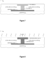
- Figure 7 illustrates processing of the semiconductor structure 7 subsequent to Figure 6 after forming a second polyimide layer 20 in the defined metal line opening 19 in accordance with selected embodiments of the present disclosure.
- the second polyimide layer 20 may be formed after stripping or removing the second patterned photoresist layer 17, and then using a damascene or inlaid process to form the second polyimide layer 20 to make direct contact with the underlying first polyimide layer 16.
- the second polyimide layer 20 may be formed by depositing with a spin-coating process or otherwise forming any suitable polyimide material over the semiconductor structure to completely fill the metal line opening 19 along with the upper horizontal surfaces of the first ILD1 layer 12.
- a planarization process is applied to remove excess polyimide material from the upper horizontal surfaces of the first ILD1 layer 12, thereby planarizing the second polyimide layer 20.
- Figure 8 illustrates processing of the semiconductor structure 8 subsequent to Figure 7 after applying a laser irradiation source 21 to directly convert the first and second polyimide layers 16, 20 into, respectively, a graphene via structure 22 and graphene wiring line 23, thereby forming a graphene interconnect structure 22-23 in accordance with selected embodiments of the present disclosure. While any suitable laser irradiation source 21 process may be used, the lasers ranging from infrared, ultraviolet, and visible ranges may be employed to provide a laser-induced graphene process which synthesizes the graphene interconnect structure 22-23.
- an ultraviolet laser may be employed to directly lase polyimide (PI) plastic films into 3D porous graphene material as a one-step method without the need for high-temperature reaction conditions, solvent, or subsequent treatments. Since the first and second polyimide layers 16, 20 have different depth profiles in the first ILD1 layer 12, the application of the laser irradiation source 21 should be controlled to selectively apply the required energy dosage for converting both the first and second polyimide layers 16, 20 into graphene.
- PI polyimide
- the laser scanning operations may be controlled to apply a first set of laser pulses which are positioned with sufficient energy to convert the entirety of the first polyimide layer 16 into the graphene via structure 22, and to apply a second set of laser pulses which are positioned with sufficient energy to convert the entirety of the second polyimide layer 20 into the graphene wiring line structure 23.
- the graphene interconnect structures 22-23 are selectively formed in the semiconductor structure 8 to provide reduced electrical resistivity and processing complexity as compared to existing techniques which use metal conductors (e.g., copper or nickel) to form the conductive interconnect structures.
- a single inlaid interconnect process may be used to separately form and fill the via etch opening 15 and the metal line opening 19.
- other embodiments of the present disclosure may use a dual inlaid interconnect process whereby a via etch opening and the metal line opening are sequentially formed in the first ILD1 layer 12, and then subsequently filled with one or more polyimide layers using a single deposition step, followed by a planarization or CMP step to planarize the deposited polyimide layer(s).
- the planarization or CMP step can occur after forming the graphene interconnect structure(s).
- a second graphene interconnect structure may be formed in a second inter-layer dielectric (ILD2) layer that is formed on the first ILD ILD1 layer by selectively etching a via etch opening and next level metal line opening in the second ILD2 layer which expose the graphene interconnect structures 22-23, filling the via etch opening and next level metal line opening with one or more polyimide layers, and then selectively applying a laser beam at the appropriate energy dose and intensity to directly convert the one or more polyimide layers into the second graphene interconnect structure.
- ILD2 inter-layer dielectric
- the last or topmost metal layers in the semiconductor structure can be formed with any conductive material, such as laser-induced graphene, aluminum, copper, tantalum, tungsten, tantalum nitride, tungsten nitride, titanium, titanium nitride, or the like and combinations of the above.
- each of the last metal layers is coupled to one or more integrated circuit elements (not shown) in the substrate 10 via the intervening graphene interconnect structures (e.g., 22, 23) formed within ILD layers of an interconnect stack which may be formed with any insulating material.
- each may be constructed within a constituent ILD layer in the interconnect stack by using a damascene process to form polyimide structures which are converted with laser irradiation pulses into graphene structures as disclosed herein.
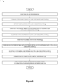
- FIG. 9 there is illustrated a simplified process flow 9 for fabricating a graphene interconnect structure in accordance with selected embodiments of the present disclosure.
- selected embodiments of the graphene interconnect fabrication methodology are described with reference to an example back-end-of-line fabrication process, it will be appreciated by persons skilled in the art that the sequence of illustrated steps may be used in any suitable stage of the device fabrication process, and may be modified, reduced or augmented in keeping with the disclosure of the present invention.
- the methodology of the present disclosure may be thought of as performing the identified sequence of steps in the order depicted in Figure 9 , though the steps may also be performed in parallel, in a different order, or as independent operations that are combined.
- the disclosed fabrication methodology begins with one or more front-end-of-line (FEOL) processing steps 92 which are used to fabricate one or more integrated circuit elements (e.g., transistors, capacitors, resistors, diodes, etc.) in a wafer substrate.
- FEOL processing is the first portion of IC fabrication where the individual components (transistors, capacitors, resistors, etc.) are patterned in the semiconductor, and generally covers everything up to (but not including) the deposition of metal interconnect layers.
- first ILD interconnects are formed over the wafer substrate with an attached first metal (M1) line.
- An example first ILD interconnect may include an initial interlayer dielectric (ILD0) layer that is formed over the integrated circuit elements by depositing, spin-coating, or otherwise forming a silicon dioxide layer.
- ILD0 initial interlayer dielectric
- a contact may be formed to extend through the initial ILD0 layer to a terminal of an integrated circuit element (e.g., a source/drain region of a transistor device), such as be selectively etching a contact opening and then filling the opening with one or more conductive via layers.
- a first metal (M1) layer may be selectively formed over the initial ILD0 layer, such as by depositing a conductive metal layer over the wafer substrate that is subsequently patterned and etched to leave the M1 layer.
- the M1 layer may be formed by selectively etching a metal line etch opening in the initial ILD0 layer, filling the metal line etch opening with one or more polyimide layers, and then selectively applying a laser beam at the appropriate energy dose and intensity to directly convert the one or more polyimide layers into a graphene M1 metal line layer.
- an ultra low-k (ULK) dielectric layer is deposited and planarized over the wafer substrate.
- An example ULK dielectric layer may be formed with a dielectric material having a dielectric constant k value of less than about 2.5 that is formed to a predetermined thickness using any suitable deposition technique, such as CVD, PECVD, PVD, ALD, AP-CVD, CBD, or any combination(s) of the above.
- Example ULK materials include, but are not limited to fluorinated amorphous diamond-like carbon (a-C:F), carbon-doped SiO 2 , Parvlene-F, Bezocycloutane (BCB), Teflon AF, or another similar ultra-low k dielectric.
- the ULK dielectric layer may be replaced with a dielectric material having a dielectric constant k value that is less than about 3.9.
- a first photoresist mask with a patterned via etch opening is formed over the ultra low-k dielectric layer.
- the first photoresist mask is formed by coating the ULK dielectric layer with a light-sensitive organic material, applying a light source with a patterned mask over the surface of the wafer substrate which blocks light so that only unmasked regions of the material will be exposed to light, and applying a solvent to develop the material so that photo-sensitive material degraded by light and the developer will dissolve away the regions that were exposed to light, leaving behind a coating where the mask was placed and an via etch opening over the ULK dielectric layer where the coating is removed.
- a via opening is selectively etched into the ultra low-k dielectric layer using the first photoresist mask.
- the ULK dielectric layer is selectively etched by using the first photoresist mask to perform a reactive-ion etching (RIE) step having suitable etch chemistry properties to selectively etch the via opening by removing the exposed portions of the underlying ULK dielectric layer to a predetermined depth which exposes the underlying M1 layer.
- RIE reactive-ion etching
- a first polyimide layer is formed in the via opening formed in the ultra low-k dielectric layer after removing the first photoresist mask.
- An example first polyimide layer may be formed with any suitable high-performance polymer material having optical and dielectric properties such that the polymer material is converted to a graphene material in direct response to laser irradiation, and may be deposited to completely fill the via opening using any suitable deposition technique, such as CVD, PECVD, PVD, ALD, AP-CVD, CBD, or any combination(s) of the above.
- Example polyimide materials include, but are not limited to, fluorinated polyimide (PI-FP, PI-FO and PI-FH) films which may be prepared using a polycondensation reaction method by incorporating p-phenylenediamine (PDA), 4-40-diaminodiphenyl ether (ODA) and 4,40-(Hexafluoroisopropylidene) bis (p-phenyleneoxy) dianiline (HFPBDA) into 4,40-(Hexafluoroisopropylidene) diphthalic anhydride (6FDA), respectively.
- PDA p-phenylenediamine
- ODA 4-40-diaminodiphenyl ether
- HFPBDA 4,40-(Hexafluoroisopropylidene) bis (p-phenyleneoxy) dianiline
- 6FDA 4,40-(Hexafluoroisopropylidene) diphthalic anhydride
- PI-FP represents 6FDA-PDA
- PI-FO represents 6FDA-ODA
- PI-FH represents 6FDA- HFBAPP, respectively.
- a second photoresist mask with a patterned metal line etch opening is formed over the ultra low-k dielectric layer.
- the second photoresist mask is formed by coating the ULK dielectric layer with a light-sensitive organic material, applying a light source with a patterned mask over the surface of the wafer substrate which selectively blocks light, and developing the material to leave a coating where the mask was placed and to leave a metal line etch opening over the ULK dielectric layer where the coating is removed.
- a metal line opening is selectively etched into the ultra low-k dielectric layer using the second photoresist mask.
- the ULK dielectric layer is selectively etched by using the second photoresist mask to perform a reactive-ion etching (RIE) step having suitable etch chemistry properties to selectively etch the metal line opening by removing the exposed portions of the underlying ULK dielectric layer to a predetermined depth which exposes the underlying first polyimide layer.
- RIE reactive-ion etching
- a second polyimide layer is formed in the metal line opening formed in the ultra low-k dielectric layer after removing the second photoresist mask.
- the second polyimide layer may be formed using any suitable deposition technique, such as CVD, PECVD, PVD, ALD, AP-CVD, CBD, or any combination(s) of the above, to deposit any suitable high-performance polymer material having optical and dielectric properties such that the polymer material is converted to a graphene material in direct response to laser irradiation.
- Example polyimide materials include, but are not limited to, fluorinated polyimide (PI-FP, PI-FO and PI-FH) films which may be prepared using a polycondensation reaction method by incorporating p-phenylenediamine (PDA), 4-40-diaminodiphenyl ether (ODA) and 4,40-(Hexafluoroisopropylidene) bis (p-phenyleneoxy) dianiline (HFPBDA) into 4,40-(Hexafluoroisopropylidene) diphthalic anhydride (6FDA), respectively.
- PDA p-phenylenediamine
- ODA 4-40-diaminodiphenyl ether
- HFPBDA 4,40-(Hexafluoroisopropylidene) bis (p-phenyleneoxy) dianiline
- 6FDA 4,40-(Hexafluoroisopropylidene) diphthalic anhydride
- a CMP or other planarization step may be applied to the first polyimide layer with the ULK dielectric layer, either directly after forming the second polyimide layer or at a subsequent stage in the fabrication process.
- the formation of the first and second polyimide layers may be performed in a single polyimide deposition step.
- a laser is applied to the first and second polyimide layers to form graphene via and metal lines.
- a laser irradiation source such as an ultraviolet laser
- the application of the laser irradiation source should be controlled to selectively apply the required energy dosage for converting both the first and second polyimide layers into graphene.
- a single-inlaid flow could be employed to decouple the laser parameters for the via from the metal line.
- the first polyimide layer could be deposited and lased to form the conductive graphene via structure, followed by depositing and lasing the second polyimide layer to form the conductive graphene wiring line structure.
- the planarization of the graphene wiring line structure can occur after lasing the second polyimide layer to form the graphene wiring line structure.
- the planarization of the graphene wiring line structure can by depositing photo-imageable polyimide and controlling the light exposure so that the upper polyimide is exposed and then selectively removed with a development process, leaving polyimide that is coplanar with the top of the ILD so that no CMP planarization would be needed.
- step 102 the fabrication process flow ends, though it will be appreciated that additional back-end-of-line processing may occur to complete the fabrication of the integrated circuit structure, such as packaging, scribe cuts, die separation, testing, etc.
- the present disclosure provides a mechanism for integrating graphene interconnects into ultra-low k dielectric layers with an exceptionally planar BEOL flow which does not need special metal, barrier, or liner layers for graphene contacts, and which circumvents the most complex and costly BEOL operations while providing the highest known conductivity.
- the disclosed mechanism for integrating graphene interconnects provides advantages to reliability and yield by reducing or eliminating stress migration, electromigration, or plasma induced damage.
- an integrated circuit structure is provided that includes a first dielectric layer formed over a first conductive contact layer.
- the integrated circuit structure is provided with a semiconductor substrate on which is formed a plurality of integrated circuit elements covered by the first dielectric layer.
- the first dielectric layer includes an ultra low-k dielectric layer and the first conductive contact layer includes a graphene contact layer.
- the disclosed methodology also includes forming an interconnect opening in the first dielectric layer which exposes at least a portion of the first conductive contact layer.
- the interconnect opening is formed in the first dielectric layer by patterning a first resist material on the first dielectric layer to form a first resist mask with a via opening over the first dielectric layer, selectively etching the via opening in the first dielectric layer using the first resist mask, patterning a second resist material on the first dielectric layer to form a second resist mask with a metal line opening over the first dielectric layer, and selectively etching the metal line opening in the first dielectric layer using the second resist mask.
- the disclosed methodology includes filling interconnect opening in the first dielectric layer with polyimide in contact the first conductive contact layer.
- a graphene interconnect structure and associated method of fabrication In the disclosed methodology, a first conductive layer is formed over a first dielectric layer. In selected embodiments, the first conductive layer is formed with a first graphene layer on the first dielectric layer which covers a plurality of integrated circuit elements formed on a semiconductor substrate. The disclosed methodology also includes forming a second dielectric layer over the first conductive layer. In selected embodiments, the second dielectric layer is formed by depositing and planarizing an ultra-low-k dielectric layer over the first conductive layer. In other selected embodiments, the second dielectric layer is formed with amorphous fluorinated diamond-like carbon (a-C:F).
- a-C:F amorphous fluorinated diamond-like carbon
- the ultra-low-k dielectric layer is fluorinated amorphous diamond-like carbon.
- the disclosed methodology includes forming a via etch opening in the second dielectric layer which exposes at least a portion of the first conductive layer.
- the via etch opening is formed in the second dielectric layer by patterning a first resist material on the second dielectric layer to form a first resist mask with a via opening over the second dielectric layer; and selectively etching the via etch opening in the second dielectric layer using the via opening in the first resist mask.
- the disclosed methodology also includes forming a wiring line etch opening in an upper portion of the second dielectric layer having a portion which overlaps with the via etch opening.
- the wiring line etch opening is formed in the upper portion of the second dielectric layer by patterning a second resist material on the second dielectric layer to form a second resist mask with a wiring line opening over the second dielectric layer; and selectively etching the wiring line etch opening in the second dielectric layer using the wiring line opening in the second resist mask.
- the disclosed methodology includes forming one or more polyimide layers to fill the via etch opening and the wiring line etch opening in the second dielectric layer.
- the one or more polyimide layers are formed by filling the via etch opening and the wiring line etch opening in the second dielectric layer with one or more first polyimide layers using a first deposition process; and planarizing the one or more first polyimide layers with a top surface of the second dielectric layer.
- the disclosed methodology also includes applying irradiation from a laser source to directly convert the one or more polyimide layers into the graphene interconnect structure comprising a graphene wiring line formed in the wiring line etch opening and a graphene via structure formed in the via etch opening to directly, electrically connect the graphene wiring line to the first conductive layer.
- irradiation from a laser source is applied by applying a laser irradiation source to one or more first polyimide layers located in the via etch opening to form the graphene via structure in the second dielectric layer in direct electrical contact with the first conductive layer; and applying a laser irradiation source to one or more second polyimide layers located in the wiring line etch opening to form the graphene wiring line structure in the second dielectric layer which is in direct electrical contact with the graphene via structure.
- irradiation from a femto-second UV laser source is applied to directly convert the one or more polyimide layers into the graphene interconnect structure.
- the disclosed methodology also includes planarizing the graphene wiring line with a top surface of the second dielectric layer.
- the integrated circuit includes a substrate having one or more semiconductor devices formed therein.
- the semiconductor device includes a multi-layer interconnect stack formed over the substrate to include a plurality of stacked wiring lines that are vertically separated from one another by a corresponding plurality of interlayer dielectric (ILD) layers.
- the multi-layer interconnect stack includes a first graphene wiring line in a first conductor layer, a second graphene wiring line in a second conductor layer that is separated from the first graphene wiring line by a first ILD layer, and a first graphene via structure formed in the first ILD layer to electrically connect the first graphene wiring line to the second graphene wiring line.
- first graphene wiring line, second graphene wiring line, and first graphene via structure are formed as an irradiation-induced graphene structure which does not include an underlying metal layer.
- first graphene wiring line, second graphene wiring line, and first graphene via structure are each formed as a laser-induced graphene foam structure.
- the first ILD layer is formed with amorphous fluorinated diamond-like carbon (a-C:F).
Landscapes
- Internal Circuitry In Semiconductor Integrated Circuit Devices (AREA)
- Physics & Mathematics (AREA)
- Optics & Photonics (AREA)
Applications Claiming Priority (1)
| Application Number | Priority Date | Filing Date | Title |
|---|---|---|---|
| US18/369,755 US20250096113A1 (en) | 2023-09-18 | 2023-09-18 | Semiconductor wafer fabrication with polyimide to graphene conversion |
Publications (2)
| Publication Number | Publication Date |
|---|---|
| EP4525031A1 true EP4525031A1 (fr) | 2025-03-19 |
| EP4525031B1 EP4525031B1 (fr) | 2026-03-11 |
Family
ID=92712475
Family Applications (1)
| Application Number | Title | Priority Date | Filing Date |
|---|---|---|---|
| EP24199255.1A Active EP4525031B1 (fr) | 2023-09-18 | 2024-09-09 | Fabrication de plaquettes semi-conductrices avec conversion de polyimide en graphène |
Country Status (3)
| Country | Link |
|---|---|
| US (1) | US20250096113A1 (fr) |
| EP (1) | EP4525031B1 (fr) |
| CN (1) | CN119650513A (fr) |
Families Citing this family (1)
| Publication number | Priority date | Publication date | Assignee | Title |
|---|---|---|---|---|
| CN120914114B (zh) * | 2025-10-10 | 2026-01-27 | 甬矽半导体(宁波)有限公司 | 衬底布线方法和衬底封装结构 |
Citations (2)
| Publication number | Priority date | Publication date | Assignee | Title |
|---|---|---|---|---|
| US20130015583A1 (en) * | 2011-07-15 | 2013-01-17 | Infineon Technologies Ag | Chip Comprising an Integrated Circuit, Fabrication Method and Method for Locally Rendering a Carbonic Layer Conductive |
| CN115101505A (zh) * | 2022-06-16 | 2022-09-23 | 北京京东方技术开发有限公司 | 一种基板、制备方法及电子装置 |
Family Cites Families (7)
| Publication number | Priority date | Publication date | Assignee | Title |
|---|---|---|---|---|
| WO2004051726A1 (fr) * | 2002-11-29 | 2004-06-17 | Nec Corporation | Dispositif a semiconducteur et procede de fabrication |
| TWI432595B (zh) * | 2010-04-30 | 2014-04-01 | Winsky Technology Ltd | 基板塗層及其形成方法 |
| CN112479189B (zh) * | 2014-02-17 | 2024-07-09 | 威廉马歇莱思大学 | 激光诱导的石墨烯材料和它们在电子装置中的用途 |
| CN105720004B (zh) * | 2014-12-04 | 2018-12-21 | 中芯国际集成电路制造(上海)有限公司 | 半导体结构的形成方法 |
| KR101795783B1 (ko) * | 2016-06-10 | 2017-12-01 | 광주과학기술원 | 금속-그래핀 이종 접합 금속 배선, 이의 형성방법 및 이를 포함하는 반도체 소자 |
| US10164018B1 (en) * | 2017-05-30 | 2018-12-25 | Taiwan Semiconductor Manufacturing Co., Ltd. | Semiconductor interconnect structure having graphene-capped metal interconnects |
| US11094631B2 (en) * | 2018-10-25 | 2021-08-17 | Taiwan Semiconductor Manufacturing Co., Ltd. | Graphene layer for reduced contact resistance |
-
2023
- 2023-09-18 US US18/369,755 patent/US20250096113A1/en active Pending
-
2024
- 2024-09-09 EP EP24199255.1A patent/EP4525031B1/fr active Active
- 2024-09-13 CN CN202411281978.XA patent/CN119650513A/zh active Pending
Patent Citations (2)
| Publication number | Priority date | Publication date | Assignee | Title |
|---|---|---|---|---|
| US20130015583A1 (en) * | 2011-07-15 | 2013-01-17 | Infineon Technologies Ag | Chip Comprising an Integrated Circuit, Fabrication Method and Method for Locally Rendering a Carbonic Layer Conductive |
| CN115101505A (zh) * | 2022-06-16 | 2022-09-23 | 北京京东方技术开发有限公司 | 一种基板、制备方法及电子装置 |
Also Published As
| Publication number | Publication date |
|---|---|
| EP4525031B1 (fr) | 2026-03-11 |
| CN119650513A (zh) | 2025-03-18 |
| US20250096113A1 (en) | 2025-03-20 |
Similar Documents
| Publication | Publication Date | Title |
|---|---|---|
| JP3196203B2 (ja) | 半導体素子の形成方法 | |
| US10886176B2 (en) | Self-aligned interconnect patterning for back-end-of-line (BEOL) structures including self-aligned via through the underlying interlevel metal layer | |
| US7439172B2 (en) | Circuit structure with low dielectric constant regions and method of forming same | |
| CN105489590B (zh) | 嵌入式金属-绝缘体-金属电容器 | |
| JPH1174356A (ja) | 改良二重ダマスク構造体 | |
| US9136164B2 (en) | Semiconductor device and fabrication method | |
| EP4525031B1 (fr) | Fabrication de plaquettes semi-conductrices avec conversion de polyimide en graphène | |
| EP4525039A1 (fr) | Fabrication de tranche de semi-conducteur avec des caractéristiques de graphène définies par exposition | |
| US20070232048A1 (en) | Damascene interconnection having a SiCOH low k layer | |
| US20060118955A1 (en) | Robust copper interconnection structure and fabrication method thereof | |
| TW202405890A (zh) | 半導體裝置結構的形成方法 | |
| US20250316496A1 (en) | Film deposition for patterning process | |
| US9837351B1 (en) | Avoiding gate metal via shorting to source or drain contacts | |
| US7282436B2 (en) | Plasma treatment for silicon-based dielectrics | |
| US9117887B2 (en) | Fabrication method of semiconductor device | |
| US11158536B2 (en) | Patterning line cuts before line patterning using sacrificial fill material | |
| JP2003303880A (ja) | 積層層間絶縁膜構造を利用した配線構造およびその製造方法 | |
| KR100613390B1 (ko) | 금속 배선된 반도체 소자 및 반도체 소자 금속 배선 형성방법 | |
| US20070222076A1 (en) | Single or dual damascene structure reducing or eliminating the formation of micro-trenches arising from lithographic misalignment | |
| US7251799B2 (en) | Metal interconnect structure for integrated circuits and a design rule therefor | |
| US11315872B1 (en) | Self-aligned top via | |
| US20250336718A1 (en) | Low-k interconnect dielectric by selective implantation | |
| US11302571B2 (en) | Cut integration for subtractive first metal line with bottom up second metal line | |
| CN117012756A (zh) | 半导体结构及其形成方法 | |
| CN102832166B (zh) | 包含阻障件抛光停止层的集成电路及其制造方法 |
Legal Events
| Date | Code | Title | Description |
|---|---|---|---|
| PUAI | Public reference made under article 153(3) epc to a published international application that has entered the european phase |
Free format text: ORIGINAL CODE: 0009012 |
|
| STAA | Information on the status of an ep patent application or granted ep patent |
Free format text: STATUS: THE APPLICATION HAS BEEN PUBLISHED |
|
| AK | Designated contracting states |
Kind code of ref document: A1 Designated state(s): AL AT BE BG CH CY CZ DE DK EE ES FI FR GB GR HR HU IE IS IT LI LT LU LV MC ME MK MT NL NO PL PT RO RS SE SI SK SM TR |
|
| STAA | Information on the status of an ep patent application or granted ep patent |
Free format text: STATUS: REQUEST FOR EXAMINATION WAS MADE |
|
| 17P | Request for examination filed |
Effective date: 20250919 |
|
| GRAP | Despatch of communication of intention to grant a patent |
Free format text: ORIGINAL CODE: EPIDOSNIGR1 |
|
| RIC1 | Information provided on ipc code assigned before grant |
Ipc: H01L 21/768 20060101AFI20250930BHEP Ipc: H01L 23/532 20060101ALI20250930BHEP |
|
| STAA | Information on the status of an ep patent application or granted ep patent |
Free format text: STATUS: GRANT OF PATENT IS INTENDED |
|
| INTG | Intention to grant announced |
Effective date: 20251105 |
|
| GRAS | Grant fee paid |
Free format text: ORIGINAL CODE: EPIDOSNIGR3 |
|
| GRAA | (expected) grant |
Free format text: ORIGINAL CODE: 0009210 |
|
| STAA | Information on the status of an ep patent application or granted ep patent |
Free format text: STATUS: THE PATENT HAS BEEN GRANTED |
|
| AK | Designated contracting states |
Kind code of ref document: B1 Designated state(s): AL AT BE BG CH CY CZ DE DK EE ES FI FR GB GR HR HU IE IS IT LI LT LU LV MC ME MK MT NL NO PL PT RO RS SE SI SK SM TR |
|
| REG | Reference to a national code |
Ref country code: CH Ref legal event code: F10 Free format text: ST27 STATUS EVENT CODE: U-0-0-F10-F00 (AS PROVIDED BY THE NATIONAL OFFICE) Effective date: 20260311 Ref country code: GB Ref legal event code: FG4D |
|
| REG | Reference to a national code |
Ref country code: DE Ref legal event code: R096 Ref document number: 602024003128 Country of ref document: DE |
|
| REG | Reference to a national code |
Ref country code: IE Ref legal event code: FG4D |
|
| PG25 | Lapsed in a contracting state [announced via postgrant information from national office to epo] |
Ref country code: RS Free format text: LAPSE BECAUSE OF FAILURE TO SUBMIT A TRANSLATION OF THE DESCRIPTION OR TO PAY THE FEE WITHIN THE PRESCRIBED TIME-LIMIT Effective date: 20260611 |
|
| PG25 | Lapsed in a contracting state [announced via postgrant information from national office to epo] |
Ref country code: ES Free format text: LAPSE BECAUSE OF FAILURE TO SUBMIT A TRANSLATION OF THE DESCRIPTION OR TO PAY THE FEE WITHIN THE PRESCRIBED TIME-LIMIT Effective date: 20260311 |
|
| PG25 | Lapsed in a contracting state [announced via postgrant information from national office to epo] |
Ref country code: GR Free format text: LAPSE BECAUSE OF FAILURE TO SUBMIT A TRANSLATION OF THE DESCRIPTION OR TO PAY THE FEE WITHIN THE PRESCRIBED TIME-LIMIT Effective date: 20260612 |
|
| REG | Reference to a national code |
Ref country code: LT Ref legal event code: MG9D |
|
| PG25 | Lapsed in a contracting state [announced via postgrant information from national office to epo] |
Ref country code: LT Free format text: LAPSE BECAUSE OF FAILURE TO SUBMIT A TRANSLATION OF THE DESCRIPTION OR TO PAY THE FEE WITHIN THE PRESCRIBED TIME-LIMIT Effective date: 20260311 |
|
| PG25 | Lapsed in a contracting state [announced via postgrant information from national office to epo] |
Ref country code: NO Free format text: LAPSE BECAUSE OF FAILURE TO SUBMIT A TRANSLATION OF THE DESCRIPTION OR TO PAY THE FEE WITHIN THE PRESCRIBED TIME-LIMIT Effective date: 20260611 |
|
| PG25 | Lapsed in a contracting state [announced via postgrant information from national office to epo] |
Ref country code: SE Free format text: LAPSE BECAUSE OF FAILURE TO SUBMIT A TRANSLATION OF THE DESCRIPTION OR TO PAY THE FEE WITHIN THE PRESCRIBED TIME-LIMIT Effective date: 20260311 Ref country code: FI Free format text: LAPSE BECAUSE OF FAILURE TO SUBMIT A TRANSLATION OF THE DESCRIPTION OR TO PAY THE FEE WITHIN THE PRESCRIBED TIME-LIMIT Effective date: 20260311 |
|
| REG | Reference to a national code |
Ref country code: NL Ref legal event code: MP Effective date: 20260311 |
|
| PG25 | Lapsed in a contracting state [announced via postgrant information from national office to epo] |
Ref country code: HR Free format text: LAPSE BECAUSE OF FAILURE TO SUBMIT A TRANSLATION OF THE DESCRIPTION OR TO PAY THE FEE WITHIN THE PRESCRIBED TIME-LIMIT Effective date: 20260311 |
|
| PG25 | Lapsed in a contracting state [announced via postgrant information from national office to epo] |
Ref country code: LV Free format text: LAPSE BECAUSE OF FAILURE TO SUBMIT A TRANSLATION OF THE DESCRIPTION OR TO PAY THE FEE WITHIN THE PRESCRIBED TIME-LIMIT Effective date: 20260311 |
|
| PG25 | Lapsed in a contracting state [announced via postgrant information from national office to epo] |
Ref country code: BG Free format text: LAPSE BECAUSE OF FAILURE TO SUBMIT A TRANSLATION OF THE DESCRIPTION OR TO PAY THE FEE WITHIN THE PRESCRIBED TIME-LIMIT Effective date: 20260311 |