EP4525059A1 - Cellule solaire à hétérojonction, son procédé de préparation et dispositif de génération d'énergie - Google Patents
Cellule solaire à hétérojonction, son procédé de préparation et dispositif de génération d'énergie Download PDFInfo
- Publication number
- EP4525059A1 EP4525059A1 EP22941560.9A EP22941560A EP4525059A1 EP 4525059 A1 EP4525059 A1 EP 4525059A1 EP 22941560 A EP22941560 A EP 22941560A EP 4525059 A1 EP4525059 A1 EP 4525059A1
- Authority
- EP
- European Patent Office
- Prior art keywords
- solar cell
- sccm
- layer
- silicon
- wafer substrate
- Prior art date
- Legal status (The legal status is an assumption and is not a legal conclusion. Google has not performed a legal analysis and makes no representation as to the accuracy of the status listed.)
- Pending
Links
Images

Classifications
-
- C—CHEMISTRY; METALLURGY
- C30—CRYSTAL GROWTH
- C30B—SINGLE-CRYSTAL GROWTH; UNIDIRECTIONAL SOLIDIFICATION OF EUTECTIC MATERIAL OR UNIDIRECTIONAL DEMIXING OF EUTECTOID MATERIAL; REFINING BY ZONE-MELTING OF MATERIAL; PRODUCTION OF A HOMOGENEOUS POLYCRYSTALLINE MATERIAL WITH DEFINED STRUCTURE; SINGLE CRYSTALS OR HOMOGENEOUS POLYCRYSTALLINE MATERIAL WITH DEFINED STRUCTURE; AFTER-TREATMENT OF SINGLE CRYSTALS OR A HOMOGENEOUS POLYCRYSTALLINE MATERIAL WITH DEFINED STRUCTURE; APPARATUS THEREFOR
- C30B31/00—Diffusion or doping processes for single crystals or homogeneous polycrystalline material with defined structure; Apparatus therefor
- C30B31/06—Diffusion or doping processes for single crystals or homogeneous polycrystalline material with defined structure; Apparatus therefor by contacting with diffusion material in the gaseous state
- C30B31/18—Controlling or regulating
- C30B31/185—Pattern diffusion, e.g. by using masks
-
- H—ELECTRICITY
- H10—SEMICONDUCTOR DEVICES; ELECTRIC SOLID-STATE DEVICES NOT OTHERWISE PROVIDED FOR
- H10F—INORGANIC SEMICONDUCTOR DEVICES SENSITIVE TO INFRARED RADIATION, LIGHT, ELECTROMAGNETIC RADIATION OF SHORTER WAVELENGTH OR CORPUSCULAR RADIATION
- H10F71/00—Manufacture or treatment of devices covered by this subclass
- H10F71/129—Passivating
-
- C—CHEMISTRY; METALLURGY
- C30—CRYSTAL GROWTH
- C30B—SINGLE-CRYSTAL GROWTH; UNIDIRECTIONAL SOLIDIFICATION OF EUTECTIC MATERIAL OR UNIDIRECTIONAL DEMIXING OF EUTECTOID MATERIAL; REFINING BY ZONE-MELTING OF MATERIAL; PRODUCTION OF A HOMOGENEOUS POLYCRYSTALLINE MATERIAL WITH DEFINED STRUCTURE; SINGLE CRYSTALS OR HOMOGENEOUS POLYCRYSTALLINE MATERIAL WITH DEFINED STRUCTURE; AFTER-TREATMENT OF SINGLE CRYSTALS OR A HOMOGENEOUS POLYCRYSTALLINE MATERIAL WITH DEFINED STRUCTURE; APPARATUS THEREFOR
- C30B29/00—Single crystals or homogeneous polycrystalline material with defined structure characterised by the material or by their shape
- C30B29/02—Elements
- C30B29/06—Silicon
-
- C—CHEMISTRY; METALLURGY
- C30—CRYSTAL GROWTH
- C30B—SINGLE-CRYSTAL GROWTH; UNIDIRECTIONAL SOLIDIFICATION OF EUTECTIC MATERIAL OR UNIDIRECTIONAL DEMIXING OF EUTECTOID MATERIAL; REFINING BY ZONE-MELTING OF MATERIAL; PRODUCTION OF A HOMOGENEOUS POLYCRYSTALLINE MATERIAL WITH DEFINED STRUCTURE; SINGLE CRYSTALS OR HOMOGENEOUS POLYCRYSTALLINE MATERIAL WITH DEFINED STRUCTURE; AFTER-TREATMENT OF SINGLE CRYSTALS OR A HOMOGENEOUS POLYCRYSTALLINE MATERIAL WITH DEFINED STRUCTURE; APPARATUS THEREFOR
- C30B31/00—Diffusion or doping processes for single crystals or homogeneous polycrystalline material with defined structure; Apparatus therefor
- C30B31/06—Diffusion or doping processes for single crystals or homogeneous polycrystalline material with defined structure; Apparatus therefor by contacting with diffusion material in the gaseous state
- C30B31/18—Controlling or regulating
-
- H—ELECTRICITY
- H10—SEMICONDUCTOR DEVICES; ELECTRIC SOLID-STATE DEVICES NOT OTHERWISE PROVIDED FOR
- H10F—INORGANIC SEMICONDUCTOR DEVICES SENSITIVE TO INFRARED RADIATION, LIGHT, ELECTROMAGNETIC RADIATION OF SHORTER WAVELENGTH OR CORPUSCULAR RADIATION
- H10F10/00—Individual photovoltaic cells, e.g. solar cells
- H10F10/10—Individual photovoltaic cells, e.g. solar cells having potential barriers
- H10F10/14—Photovoltaic cells having only PN homojunction potential barriers
-
- H—ELECTRICITY
- H10—SEMICONDUCTOR DEVICES; ELECTRIC SOLID-STATE DEVICES NOT OTHERWISE PROVIDED FOR
- H10F—INORGANIC SEMICONDUCTOR DEVICES SENSITIVE TO INFRARED RADIATION, LIGHT, ELECTROMAGNETIC RADIATION OF SHORTER WAVELENGTH OR CORPUSCULAR RADIATION
- H10F71/00—Manufacture or treatment of devices covered by this subclass
- H10F71/121—The active layers comprising only Group IV materials
-
- H—ELECTRICITY
- H10—SEMICONDUCTOR DEVICES; ELECTRIC SOLID-STATE DEVICES NOT OTHERWISE PROVIDED FOR
- H10F—INORGANIC SEMICONDUCTOR DEVICES SENSITIVE TO INFRARED RADIATION, LIGHT, ELECTROMAGNETIC RADIATION OF SHORTER WAVELENGTH OR CORPUSCULAR RADIATION
- H10F77/00—Constructional details of devices covered by this subclass
- H10F77/70—Surface textures, e.g. pyramid structures
- H10F77/703—Surface textures, e.g. pyramid structures of the semiconductor bodies, e.g. textured active layers
Definitions
- the present disclosure relates to the field of cells, in particular to a solar cell and a preparation method therefor and an application thereof.
- Interdigitated back contact solar cell can further optimize a trapping and passivation performance of the front surface without considering a contact resistance on the front side due to a particularity (metal electrodes are located on a back side of the cell, and positive and negative electrodes are arranged in an interdigitated manner) of structure of components thereof.
- a back portion can optimize the metal grid electrode, thus reducing a series resistance and increasing a filling factor.
- a conventional back contact solar cell structure has a tunneling oxygen passivation contact (TOPCon) structure, and a passivation structure includes an ultrathin silicon oxide layer and a heavily doped polysilicon layer to passivate a back surface of the cell.
- a passivation mechanism of the structure is as follows: the ultrathin silicon oxide is directly in contact with a silicon wafer substrate to neutralize dangling bonds on a surface of the silicon and perform excellent chemical passivation. Due to a difference of Fermi energy level between a heavily doped polysilicon layer and a silicon wafer substrate, so that energy band bending is caused on the surface of the silicon wafer substrate, which can more effectively block the passage of minority carriers without affecting the transmission of majority carriers, thereby achieving selective collection of carriers.
- the carriers can be directly and efficiently transmitted in one-dimensional longitudinal direction through an oxide layer, so that a current transmission path is the shortest, the recombination caused by the carriers in the two-dimensional transmission process is avoided, the series resistance of the cell is reduced, the cell has a higher filling factor, and thus higher photoelectric conversion efficiency can be obtained.
- a doping layer is prepared by low pressure chemical vapor deposition (LPCVD) and plasma enhanced chemical vapor deposition (PECVD), and since the doping layer is relatively thick, a certain thickness of doping layer material will be coated around the front side of the cell using the above deposition method.
- a formed wrap plating material will greatly reduce the conversion efficiency of the cell, resulting in a certain degree of leakage.
- phosphorus diffusion in a LPCVD route also affects the front side of the cell, so that a wet process is usually added to remove these wrap plating.
- adding the wet process will not only increase equipment and labor costs, but may also affect an appearance of the front side of the cell itself due to the wet process, which will also affect the cell conversion efficiency.
- the present disclosure provides a preparation method for a solar cell, including the following steps:
- a temperature for forming the doping layer in step S20 is 200°C to 700°C.
- the doping gas source is selected from at least one of phosphorane, diborane, trimethylborane, and boron trifluoride.
- the preparation method for the solar cell further includes a step of annealing after step S20 and prior to step S30.
- an annealing temperature is 800°C to 950°C, and an annealing time is 30 min to 50 min.
- the silicon oxide layer is formed on the first surface by plasma enhanced chemical vapor deposition, low pressure chemical vapor deposition, or thermal oxygen.
- a thickness of the silicon oxide layer 0.5 nm to 2.5 nm.
- the mask layer is formed on the doping layer by thermal oxygen, plasma enhanced chemical vapor deposition, or low pressure chemical vapor deposition.
- a thickness of the mask layer is 5 nm to 100 nm.
- the preparation method for the solar cell further includes: after preparing the silicon wafer substrate with a textured surface, forming a first passivation film layer and a first anti-reflection film layer sequentially on the first surface of the silicon wafer substrate with the textured surface.
- the preparation method for the solar cell further includes: after preparing the silicon wafer substrate with a textured surface, forming a second passivation film layer and a second anti-reflection film layer sequentially on the second surface of the silicon wafer substrate with the textured surface.
- the preparation method for the solar cell further includes, after step S50, a step S60, forming a hole on the patterned region on the first surface by patterning using a laser, and preparing a first electrode and a second electrode by screen printing.
- a solar cell is further provided, which is prepared by a preparation method including the following steps:
- the doping gas source is selected from at least one of phosphorane, diborane, trimethylborane, and boron trifluoride.
- the preparation method further includes a step of annealing after step S20 and prior to step S30.
- an annealing temperature is 800°C to 950°C, and an annealing time is 30 min to 50 min.
- the silicon oxide layer is formed on the first surface by plasma enhanced chemical vapor deposition, low pressure chemical vapor deposition, or thermal oxygen.
- a thickness of the silicon oxide layer 0.5 nm to 2.5 nm.
- the mask layer is formed on the doping layer by thermal oxygen, plasma enhanced chemical vapor deposition, or low pressure chemical vapor deposition.
- a thickness of the mask layer is 5 nm to 100 nm.
- the preparation method further includes: after preparing the silicon wafer substrate with a textured surface, forming a first passivation film layer and a first anti-reflection film layer sequentially on the first surface of the silicon wafer substrate with the textured surface.
- the preparation method further includes: after preparing the silicon wafer substrate with a textured surface, forming a second passivation film layer and a second anti-reflection film layer sequentially on the second surface of the silicon wafer substrate with the textured surface.
- the preparation method further includes, after step S50, a step S60, forming a hole on the patterned region on the first surface by patterning using a laser, and preparing a first electrode and a second electrode by screen printing.
- a photovoltaic system which includes a solar cell assembly and an auxiliary device, the solar cell assembly including the solar cell as described in any of the aforementioned embodiments.
- the present disclosure may be implemented in many different forms and is not limited to the embodiments described herein. On the contrary, the purpose of providing these embodiments is to make the public content of the present disclosure more thoroughly and comprehensively understood. Certainly, they are merely examples and are not intended to limit the present disclosure.
- reference numerals and/or letters may be repeated in different embodiments of the present disclosure. This repetition is for purposes of simplicity and clarity and does not in itself indicate a relationship between the various embodiments and/or arrangements discussed.
- first and second are used for descriptive purposes only and cannot be understood as indicating or implying relative importance or implicitly indicating the number or order of indicated technical features. Therefore, features defined as “first” and “second” may explicitly or implicitly include at least one of these features.
- plural means at least two, such as two, three, etc., unless otherwise expressly and specifically limited.
- severeal means at least one, for example, one, two, etc., unless otherwise expressly and specifically limited.
- the range is considered continuous and includes the minimum and maximum values of the range and every value between such minimum and maximum values. Further, when the range refers to integers, every integer between the minimum value and the maximum value of the range is included. Further, when multiple ranges are provided to describe a feature or characteristics, the ranges may be combined. In other words, unless otherwise indicated, all ranges disclosed herein shall be understood to include any and all subranges subsumed therein.
- the present disclosure provides a preparation method for a solar cell 10 as shown in FIG. 1 , which includes the following steps.
- Step S10 A silicon wafer substrate 110 is provided, and the silicon wafer substrate 110 has a first surface and a second surface opposite to the first surface.
- the first surface is a backlight surface of the cell, which is also called a back surface
- the second surface is a light-receiving surface of the cell, which is also called a front surface.
- step S10 the silicon wafer substrate 110 is further subjected to de-damage treatment, polishing treatment, and cleaning treatment.
- the de-damage treatment includes a treatment with a monobasic strong base containing a substance at a concentration of 0.6 mol/L to 0.8 mol/L at 50°C to 70°C.
- a temperature of the de-damage treatment may be, but is not limited to, 50°C, 55°C, 60°C, 65°C, or 70°C.
- a solution for the de-damage treatment is a mixed solution of 46% by mass of sodium hydroxide solution and water at a volume ratio of 4:96 to 6:94.
- the polishing treatment includes a treatment with a monobasic strong base solution containing a substance at a concentration of 0.6 mol/L to 0.8 mol/L at 65°C to 85°C, so that a reflectivity after polishing is 20% to 40%.
- the reflectivity after polishing may be, but is not limited to, 20%, 25%, 30%, 35% or 40%.
- the reflectivity of the silicon wafer substrate after polishing is 30%.
- the cleaning treatment includes cleaning with a mixed solution of hydrofluoric acid and hydrochloric acid, and deionized water in sequence, and drying.
- Step S20 A silicon-containing film 123 is formed on the first surface of the silicon wafer substrate 110.
- the silicon-containing film includes a silicon oxide layer 121, a doping layer 122, and a mask layer that are sequentially formed on the first surface of the silicon wafer substrate 110.
- the silicon oxide layer 121 having a thickness of 0.5 nm to 2.5 nm is formed on the silicon wafer substrate by plasma enhanced chemical vapor deposition, low pressure chemical vapor deposition, or thermal oxygen.
- the thickness of the silicon oxide layer 121 may be, but is not limited to, 0.5 nm, 1 nm, 2 nm, or 2.5 nm.
- the silicon oxide layer 121 is preferably formed by plasma enhanced chemical vapor deposition.
- the step of forming the silicon oxide layer 121 in the step S10 includes: introducing silane gas at a flow rate of 1000 sccm to 5000 sccm and introducing hydrogen gas at a flow rate of 6000 sccm to 15000 sccm.
- glow discharge is performed at a temperature of 350°C to 600°C, a power supply of 9 KW to 12 KW, and a plasma pulse on-off ratio of 1:100 ms to form a silicon oxide layer 121 on the formed substrate.
- the flow rate of the silane gas is 2500 sccm to 3000 sccm and the flow rate of the hydrogen gas is 8000 sccm to 10000 sccm.
- the temperature for preparing the silicon oxide layer 121 is prepared is preferably 400°C to 450°C.
- the temperature for preparing the silicon oxide layer 121 may be, but is not limited to, 410°C, 420°C, 430°C, 440°C or 450°C.
- the power supply power is 9 KW to 10 KW.
- the doping layer 122 with a thickness of 30 nm to 300 nm is formed on the silicon oxide layer by a physical vapor deposition in an atmosphere containing a doping gas source and silane.
- a doping layer having a thickness of 10 nm to 30 nm is formed in an atmosphere containing a doping gas source at a flow rate of 100 sccm to 1000 sccm and silane at a flow rate of 1000 sccm to 4000 sccm
- the remaining doping layer 122 is formed in an atmosphere containing a doping gas source at a flow rate of 1500 sccm to 3000 sccm and silane at a flow rate of 1000 sccm to 4000 sccm.
- the doping layer 122 having a thickness of 10 nm to 30 nm is formed in an atmosphere containing a doping gas source at a flow rate of 200 sccm to 800 sccm and silane at a flow rate of 2000 sccm to 3600 sccm.
- the flow rate of the doping gas source may be, but is not limited to, 200 sccm, 300 sccm, 400 sccm, 500 sccm, 600 sccm, 700 sccm, or 800 sccm
- the flow rate of the silane may be, but is not limited to, 3600 sccm, 2200 sccm, 2400 sccm, 2600 sccm, 2700 sccm, 2800 sccm, 2900 sccm, 3000 sccm, 3200 sccm, 3400 sccm, or 3600 sccm.
- the remaining doping layer 122 is formed in an atmosphere containing a doping gas source at a flow rate of 2000 sccm to 3000 sccm and silane at a flow rate of 2000 sccm to 3600 sccm.
- the flow rate of the doping gas source may be, but is not limited to, 2000 sccm, 2200 sccm, 2400 sccm, 2600 sccm, 2800 sccm, or 3000 sccm
- the flow rate of the silane may be, but is not limited to, 2000 sccm, 2200 sccm, 2400 sccm, 2600 sccm, 2700 sccm, 2800 sccm, 2900 sccm, 3000 sccm, 3200 sccm, 3400 sccm, or 3600 sccm.
- a pressure in a tube during the preparation process of forming the doping layer 122 is 1Pa to 150Pa. Furthermore, a time for preparing the doping layer 122 is 5 min to 20 min.
- a temperature for forming the doping layer 122 is 200°C to 700°C, preferably 300°C to 600°C, and more preferably 400°C to 500°C.
- the temperature for forming the doping layer 122 may be, but is not limited to, 300°C, 350°C, 400°C, 450°C, 500°C, 550°C, or 600°C.
- the doping gas source is selected from at least one of phosphorane, diborane, trimethylborane, and boron trifluoride.
- the doping gas source in order to prepare the p-type doping layer 122, may be phosphorane, and in order to prepare the n-type doping layer 122, the doping gas source may be selected from at least one of diborane, trimethylborane, and boron trifluoride.
- a doping concentration of the doping layer 122 can be achieved by combining the flow rate of the doping gas source, the flow rate of the silane and a deposition temperature during the physical vapor deposition.
- the thickness of the doping layer 122 is 100 nm to 150 nm. It should be understood that the thickness of the doping layer 122 may be, but is not limited to, 100 nm, 110 nm, 120 nm, 130 nm, 140 nm, or 150 nm.
- the mask layer having a thickness of 5 nm to 100 nm is formed on the doping layer 122 by thermal oxygen, plasma enhanced chemical vapor deposition, or low pressure chemical vapor deposition.
- the thickness of the mask layer is 5 nm to 100 nm.
- the mask layer may be made of, but is not limited to, silicon oxide and silicon nitride.
- the mask layer is made of silicon oxide, and the silicon oxide layer is grown in-situ on a surface of the doping layer 122 as the mask layer by introducing oxygen at a high temperature using a thermal oxygen growth method, the temperature is 600°C to 950°C, a time is 15 min to 45 min, and a flow rate of the oxygen is 8000 sccm to 13000 sccm.
- annealing treatment is performed. It should be understood that objects of the annealing treatment includes the formed silicon oxide layer 121 and the doping layer 122, and the mask layer may also be annealed.
- an annealing temperature in step S30 is 800°C to 950°C, and an annealing time is 30 min to 50 min.
- the annealing treatment can not only convert the amorphous silicon deposited by physical vapor deposition into polycrystalline silicon, so that crystal grains grow and become larger, but also can make the mask layer more dense, and greatly improve the alkali resistance.
- the doping layer 122 is prepared by controlling the flow rate of the doping source gas using the physical vapor deposition, which not only achieves the preparation of the doping layer 122, but also the wrap-around plating phenomenon occurring on the front surface of the substrate can be further effectively reduced.
- the silicon-containing film 123 is prepared and the patterned region is formed by a laser processing, no additional process is required to remove the redundant material of the doping layer 122 generated by the wrap plating, thereby effectively reducing the process of preparing the cell, such as a wet process, without affecting a cell conversion efficiency of and the appearance of the front surface of the cell.
- Step S30 the silicon-containing film 123 on the first surface is patterned by a laser to form a patterned region 111 on the first surface of the silicon wafer substrate 110.
- a picosecond laser is used to remove the silicon-containing film 123 in a partial region on the first surface of the silicon wafer substrate 110 using a nano-laser of ultraviolet light 355 nm or 532 nm to form the patterned region 111 having a width of 300 ⁇ m to 500 ⁇ m, and a part of the silicon-containing film in the patterned region 111 is removed or destroyed to make it more susceptible to corrosion by alkaline solutions.
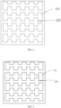
- FIG. 2 is a bottom view of the patterned region 111 after the silicon-containing film 123 is patterned.
- Step S40 the silicon wafer substrate 110 having the silicon-containing film 123 and the patterned region 111 is subjected to texturing treatment.
- a step of treating the mask layer material coated on the second surface of the substrate 110 with a hydrofluoric acid solution having a concentration of 4 mol/L to 6 mol/L prior to texturing is also included.
- the first surface of the substrate 110 is placed horizontally away from the hydrofluoric acid solution, and the first surface of the substrate 110 is covered with deionized water to avoid damaging the silicon oxide mask layer on the first surface due to contact with the hydrofluoric acid solution.
- the second surface of the substrate 110 is in contact with the hydrofluoric acid solution to remove the silicon oxide mask layer generated by the wrap plating, and the cleaning time is 60s to 240s.
- the hydrofluoric acid solution is prepared by mixing hydrofluoric acid with a mass fraction of 49% and water in a volume ratio of (10 to 30): (70 to 90).
- the hydrofluoric acid with a mass fraction of 49% and water in a ratio of 20:80 is mixed to prepare the hydrofluoric acid solution.
- a pretreated silicon wafer substrate 110 is subjected to a texturing treatment in which the silicon wafer substrate 110 having the silicon-containing film 123 and the patterned region 111 is placed in a texturing solution containing a monobasic strong base at a concentration of 0.15 mol/L to 0.35 mol/L for texturing for 400s to 600s to prepare the silicon wafer substrate 110 having a textured surface.
- the monobasic strong base is selected from at least one of potassium hydroxide and sodium hydroxide.
- the purpose of making a pile is to form a pyramid-shaped textured surface on the second surface of the substrate 110, i.e., the light-receiving surface.
- the texturing solution may further include an additive
- the additive may be, but is not limited to, indolylpropionic acid (IPA).
- IPA indolylpropionic acid
- the additive usually does not directly participate in the chemical reaction, but has the functions of reducing the surface tension of the solution, improving the uniformity of the reaction, regulating the corrosion rate of the monobasic strong base, significantly reducing the reaction rate, and enhancing the anisotropy of the corrosion.
- the silicon wafer substrate 110 with the textured surface may be subjected to, but is not limited to, water washing, alkaline washing, water washing, acid washing, water washing and drying.
- the alkaline washing is carried out using a sodium hydroxide aqueous solution with a substance amount of 0.1% to 0.2%. Further, the acid washing removes the outermost silicon oxide mask layer on the non-patterned region beyond the patterned region 111 on the first surface of the substrate 110 using an acid solution containing hydrofluoric acid.
- the method further includes the following step S50: a first passivation film layer 130 and a first anti-reflection film layer 150 are sequentially formed on the first surface of the silicon wafer substrate 110 with the textured surface and the composite film layer 120.
- first passivation film layer 130 and the first anti-reflection film layer 150 are sequentially formed on the first surface of the silicon wafer substrate 110 with the textured surface, the silicon oxide layer 121, and the doping layer 122.
- a second passivation film and a second anti-reflection film layer 160 are sequentially formed on the second surface of the silicon wafer substrate 110 with the textured surface.
- first passivation film layer 130 and the second passivation film layer 140 may be formed by, but are not limited to, an atomic layer deposition method. Further, the first passivation film layer 130 and the second passivation film layer 140 may be made of, but are not limited to, aluminum oxide.
- a thickness of the first passivation film layer 130 is 2 nm to 25 nm.
- a thickness of the second passivation film layer 140 is 2 nm to 25 nm.
- first anti-reflection film layer 150 and the second anti-reflection film layer 160 may be formed by, but is not limited to, plasma enhanced chemical vapor deposition. Further, the first anti-reflection film layer 150 and the second anti-reflection film layer 160 may be made of, but is not limited to, at least one of silicon oxide, silicon oxynitride, and silicon nitride.
- a thickness of the first anti-reflection film layer 150 is 50 nm to 150 nm.
- a thickness of the second anti-reflection film layer 160 is 60 nm to 150 nm.
- the material of the first anti-reflection film layer 150 and the material of the second anti-reflection film layer 160 contain silicon oxide, silicon oxynitride, and silicon nitride materials, which are stacked in three layers.
- the method further includes a step S60: the patterned region on the first surface is patterned by a laser to form a hole, and a first electrode 170 and a second electrode 180 are prepared by screen printing.
- a burn-through electrode slurry is coated on the first surface except the patterned region 111, the first passivation film layer 130 and the first anti-reflection film layer 150 where the burn-through electrode slurry is coated is removed, and the burn-through electrode slurry is injected until the burn-through electrode slurry is in contact with the silicon-containing film 123 to form the first electrode 170;
- the patterned region 111 on the first surface is patterned by a laser to form a hole, the first passivation film layer 130 and the first anti-reflection film layer 150 at the hole is removed to form a second electrode contact region, and an electrode slurry is injected into the second electrode contact region to form the second electrode 180.
- the patterned region 111 on the first surface is patterned by a laser to form a hole with a width of 30 ⁇ m to 50 ⁇ m, and the passivation film layer and the anti-reflection film layer at the hole is removed to form a the first electrode 170 contact region.
- Hole regions are distributed in a dotted line or dots, as shown in FIG. 3 , which is a bottom view of the patterned region 111 after forming the hole.
- first electrode 170 and the second electrode 180 may be formed by, but not limited to, screen printing.
- the first electrode 170 in contact with the doping layer 122 does not need to be opened.
- the first electrode is preferably made of burn-through electrode slurry, which can burn through the first passivation film layer 130 and the first anti-reflection film layer 150 at a high temperature to form a contact with the doping layer 122, while the substrate 110 is only in partial contact, and non-burn-through electrode slurry is used, so that the non-burn-through electrode slurry is in contact with that substrate 110 at the at the hole by a laser.
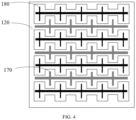
- FIG. 4 is a bottom view of the solar cell 10.
- the solar cell 10 prepared by the above preparation process is preferably a back contact cell.
- the present disclosure further provides a photovoltaic system, including a solar cell assembly and an auxiliary device.
- the solar cell assembly includes he above-mentioned solar cell 10.
- the present example provides a p-type back contact solar cell, which is prepared by the following steps:
- the solution containing potassium hydroxide or sodium hydroxide is used at a temperature of 80°C to texture the front surface and etch a laser patterned region on the back surface to remove the residual polysilicon material in the n-type doped region, and the water washing, alkali washing, and water washing are successively performed. Due to the protection of the silicon oxide mask layer, a hydrofluoric acid solution is finally used to remove the remaining silicon oxide mask layer, followed by water washing and drying.
- a 3 nm aluminum oxide film is simultaneously plated on the front surface and the back surface using an atomic layer deposition equipment in a single insertion mode to serve as a first passivation film layer and a second passivation film layer, and then a 100nm composite film layer of silicon oxide, silicon oxynitride and silicon nitride is plated on the front surface by plasma enhanced chemical vapor deposition (PECVD) to serve as a second anti-reflection film layer, and finally a 100nm composite film layer of silicon oxide, silicon oxynitride and silicon nitride is plated on the back surface by PECVD to serve as the first anti-reflection film layer.
- PECVD plasma enhanced chemical vapor deposition
- the p-type substrate region exposed after patterning the patterned region on the back surface is opened using a laser.
- the hole region is distributed in a dotted line or dots. A width of the hole is 40 ⁇ m.
- the hole region serves as an electrode contact region of the p-type substrate region.
- An electrode slurry layer containing a conductive component is formed on an electrode contact region of a p-type substrate region and an electrode contact region of an n-type doping layer on that back surface of the cell by screen printing.
- the aluminum grid line electrode is used as a positive electrode of the cell, and the silver grid line electrode is used as a cathode negative electrode of the cell.
- the present comparative example provides a p-type back contact solar cell, which is prepared by the following steps:
- the solution containing potassium hydroxide or sodium hydroxide is used at a temperature of 80°C to texture the front surface and etch a laser patterned region on the back surface to remove the residual polysilicon material in the n-type doped region, and the water washing, alkali washing, and water washing are successively performed. Due to the protection of the silicon oxide mask layer, a hydrofluoric acid solution is finally used to remove the remaining silicon oxide mask layer, followed by water washing and drying.
- a 3 nm aluminum oxide film is simultaneously plated on the front surface and the back surface using an atomic layer deposition equipment in a single insertion mode to serve as a first passivation film layer and a second passivation film layer, and then a 100nm composite film layer of silicon oxide, silicon oxynitride and silicon nitride is plated on the front surface by plasma enhanced chemical vapor deposition (PECVD) to serve as a second anti-reflection film layer, and finally a 100nm composite film layer of silicon oxide, silicon oxynitride and silicon nitride is plated on the back surface by PECVD to serve as the first anti-reflection film layer.
- PECVD plasma enhanced chemical vapor deposition
- the p-type substrate region exposed after patterning the patterned region on the back surface is opened using a laser.
- the hole region is distributed in a dotted line or dots. A width of the hole is 40 ⁇ m.
- the hole region serves as an electrode contact region of the p-type substrate region.
- An electrode slurry layer containing a conductive component is formed on an electrode contact region of a p-type substrate region and an electrode contact region of an n-type doping layer on that back surface of the cell by screen printing.
- the aluminum grid line electrode is used as a positive electrode of the cell, and the silver grid line electrode is used as a cathode negative electrode of the cell.
- the present comparative example provides a p-type back contact solar cell, which is prepared by the following steps:
- the solution containing potassium hydroxide or sodium hydroxide is used at a temperature of 80°C to texture the front surface and etch a laser patterned region on the back surface to remove the residual polysilicon material in the n-type doped region, and the water washing, alkali washing, and water washing are successively performed. Due to the protection of the silicon oxide mask layer, a hydrofluoric acid solution is finally used to remove the remaining silicon oxide mask layer, followed by water washing and drying.
- a 3 nm aluminum oxide film is simultaneously plated on the front surface and the back surface using an atomic layer deposition equipment in a single insertion mode to serve as a first passivation film layer and a second passivation film layer, and then a 100nm composite film layer of silicon oxide, silicon oxynitride and silicon nitride is plated on the front surface by plasma enhanced chemical vapor deposition (PECVD) to serve as a second anti-reflection film layer, and finally a 100nm composite film layer of silicon oxide, silicon oxynitride and silicon nitride is plated on the back surface by PECVD to serve as the first anti-reflection film layer.
- PECVD plasma enhanced chemical vapor deposition
- the p-type substrate region exposed after patterning the patterned region on the back surface is opened using a laser.
- the hole region is distributed in a dotted line or dots. A width of the hole is 40 ⁇ m.
- the hole region serves as an electrode contact region of the p-type substrate region.
- An electrode slurry layer containing a conductive component is formed on an electrode contact region of a p-type substrate region and an electrode contact region of an n-type doping layer on that back surface of the cell by screen printing.
- the aluminum grid line electrode is used as a positive electrode of the cell, and the silver grid line electrode is used as a cathode negative electrode of the cell.
- the performance of the p-type back contact solar cell provided in embodiment 1 of the present disclosure is as follows: the conversion efficiency is 24.8%, the open circuit voltage is 720mv, the current is 18A, and the filling factor FF is more than 83%.
- the p-type back-contact solar cell is finally prepared using only one flow condition to prepare the doping layer, and the cell conversion efficiency is lower than 24.2%.
- the p-type back contact solar cell prepared by introducing a high flow rate of doping source gas when preparing the doping layer has an open circuit voltage lower than 715mV, a short-circuit current lower than 18A, a filling factor FF lower than 83%, and a conversion efficiency lower than 24%.
- the conversion efficiency of conventional emitter and back-passivated PERC cells is usually between 21% and 22%.
Landscapes
- Chemical & Material Sciences (AREA)
- Engineering & Computer Science (AREA)
- Crystallography & Structural Chemistry (AREA)
- Materials Engineering (AREA)
- Metallurgy (AREA)
- Organic Chemistry (AREA)
- Photovoltaic Devices (AREA)
Applications Claiming Priority (2)
| Application Number | Priority Date | Filing Date | Title |
|---|---|---|---|
| CN202210489495.3A CN114792744B (zh) | 2022-05-07 | 2022-05-07 | 太阳电池及其制备方法和应用 |
| PCT/CN2022/143685 WO2023216628A1 (fr) | 2022-05-07 | 2022-12-30 | Cellule solaire à hétérojonction, son procédé de préparation et dispositif de génération d'énergie |
Publications (2)
| Publication Number | Publication Date |
|---|---|
| EP4525059A1 true EP4525059A1 (fr) | 2025-03-19 |
| EP4525059A4 EP4525059A4 (fr) | 2025-10-01 |
Family
ID=82461846
Family Applications (1)
| Application Number | Title | Priority Date | Filing Date |
|---|---|---|---|
| EP22941560.9A Pending EP4525059A4 (fr) | 2022-05-07 | 2022-12-30 | Cellule solaire à hétérojonction, son procédé de préparation et dispositif de génération d'énergie |
Country Status (5)
| Country | Link |
|---|---|
| US (1) | US20250126923A1 (fr) |
| EP (1) | EP4525059A4 (fr) |
| CN (1) | CN114792744B (fr) |
| AU (1) | AU2022457985B2 (fr) |
| WO (1) | WO2023216628A1 (fr) |
Families Citing this family (8)
| Publication number | Priority date | Publication date | Assignee | Title |
|---|---|---|---|---|
| JP7747902B2 (ja) | 2022-03-25 | 2025-10-01 | ジァンスー ルネルギー センチュリー フォウトウヴォルテイク テクノロジー カンパニー リミテッド | 低コストの接触パッシベーション全裏面電極太陽電池及びその製造方法 |
| CN114678446B (zh) * | 2022-03-25 | 2024-07-12 | 江苏润阳世纪光伏科技有限公司 | 一种低成本接触钝化全背电极太阳能电池及其制备方法 |
| CN114792744B (zh) * | 2022-05-07 | 2024-04-02 | 通威太阳能(成都)有限公司 | 太阳电池及其制备方法和应用 |
| CN115799172B (zh) * | 2023-02-08 | 2023-04-28 | 粤芯半导体技术股份有限公司 | 金属互连线及其制造方法 |
| CN116177550B (zh) * | 2023-03-09 | 2024-02-27 | 浙江大学 | 一种硅纳米材料的表面钝化方法及用途 |
| CN119730434A (zh) * | 2023-09-25 | 2025-03-28 | 横店集团东磁股份有限公司 | 太阳能电池及其制备方法和用电装置 |
| CN118800829A (zh) * | 2024-06-20 | 2024-10-18 | 环晟光伏(江苏)有限公司 | TOPCon电池掩膜层的制备方法及其应用 |
| DE102024120457A1 (de) * | 2024-07-18 | 2026-01-22 | Institut Für Solarenergieforschung Gmbh | Verfahren zum fertigen einer kontaktstruktur insbesondere für eine rückseitig kontaktierte solarzelle |
Family Cites Families (16)
| Publication number | Priority date | Publication date | Assignee | Title |
|---|---|---|---|---|
| WO2009117083A2 (fr) * | 2008-03-17 | 2009-09-24 | Nanopv Technologies, Inc. | Dispositif photovoltaïque et procédé |
| US8883552B2 (en) * | 2010-08-11 | 2014-11-11 | Crystal Solar Inc. | MWT architecture for thin SI solar cells |
| US9997652B2 (en) * | 2015-03-23 | 2018-06-12 | Sunpower Corporation | Deposition approaches for emitter layers of solar cells |
| US9525083B2 (en) * | 2015-03-27 | 2016-12-20 | Sunpower Corporation | Solar cell emitter region fabrication with differentiated P-type and N-type architectures and incorporating a multi-purpose passivation and contact layer |
| CN108521832A (zh) * | 2015-12-31 | 2018-09-11 | 中海阳能源集团股份有限公司 | 一种背电极异质结太阳能电池及其制备方法 |
| CN105762234B (zh) * | 2016-04-27 | 2017-12-29 | 中国科学院宁波材料技术与工程研究所 | 一种隧穿氧化层钝化接触太阳能电池及其制备方法 |
| CN110047972A (zh) * | 2019-04-12 | 2019-07-23 | 常州大学 | 一种新型多晶硅掺杂p扩散制备工艺方法 |
| CN112885925B (zh) * | 2021-02-05 | 2022-10-14 | 泰州隆基乐叶光伏科技有限公司 | 一种太阳能电池及其制作方法 |
| CN214797433U (zh) * | 2021-02-25 | 2021-11-19 | 一道新能源科技(衢州)有限公司 | 一种ibc太阳能电池 |
| CN216054727U (zh) * | 2021-06-11 | 2022-03-15 | 晶澳(扬州)太阳能科技有限公司 | 太阳能电池 |
| CN113675295B (zh) * | 2021-07-12 | 2022-07-26 | 深圳市捷佳伟创新能源装备股份有限公司 | PECVD制备硅片复合膜的方法和TOPCon电池的制备方法 |
| CN113782639A (zh) * | 2021-09-10 | 2021-12-10 | 平煤隆基新能源科技有限公司 | 一种降低晶硅太阳能电池el绕镀脏污的pecvd工艺 |
| CN113690328B (zh) * | 2021-10-25 | 2022-03-01 | 晶科能源(海宁)有限公司 | 太阳能电池及其制备方法、光伏组件 |
| CN114256385B (zh) * | 2021-12-22 | 2024-01-09 | 韩华新能源(启东)有限公司 | 一种tbc背接触太阳能电池及其制备方法 |
| CN114361295B (zh) * | 2021-12-31 | 2023-06-06 | 通威太阳能(眉山)有限公司 | 太阳能电池板、电池片及电池片的生产工艺 |
| CN114792744B (zh) * | 2022-05-07 | 2024-04-02 | 通威太阳能(成都)有限公司 | 太阳电池及其制备方法和应用 |
-
2022
- 2022-05-07 CN CN202210489495.3A patent/CN114792744B/zh active Active
- 2022-12-30 EP EP22941560.9A patent/EP4525059A4/fr active Pending
- 2022-12-30 US US18/834,069 patent/US20250126923A1/en active Pending
- 2022-12-30 AU AU2022457985A patent/AU2022457985B2/en active Active
- 2022-12-30 WO PCT/CN2022/143685 patent/WO2023216628A1/fr not_active Ceased
Also Published As
| Publication number | Publication date |
|---|---|
| EP4525059A4 (fr) | 2025-10-01 |
| WO2023216628A1 (fr) | 2023-11-16 |
| CN114792744A (zh) | 2022-07-26 |
| AU2022457985A1 (en) | 2024-08-15 |
| WO2023216628A9 (fr) | 2024-08-08 |
| US20250126923A1 (en) | 2025-04-17 |
| WO2023216628A8 (fr) | 2024-09-19 |
| CN114792744B (zh) | 2024-04-02 |
| AU2022457985B2 (en) | 2026-01-22 |
Similar Documents
| Publication | Publication Date | Title |
|---|---|---|
| EP4525059A1 (fr) | Cellule solaire à hétérojonction, son procédé de préparation et dispositif de génération d'énergie | |
| JP7368653B2 (ja) | 太陽電池及び光起電力モジュール | |
| US12342656B1 (en) | Solar cell and solar cell module | |
| US20250212550A1 (en) | Solar cell, preparation method therefor, and application thereof | |
| CN114242803A (zh) | 太阳能电池及其制备方法、光伏组件 | |
| US20080000522A1 (en) | Photovoltaic device which includes all-back-contact configuration; and related processes | |
| CN116914012A (zh) | 一种双面掺杂多晶硅钝化接触电池及其制备方法 | |
| EP4379816A1 (fr) | Cellule solaire et son procédé de fabrication | |
| CN111628052A (zh) | 一种钝化接触电池的制备方法 | |
| US20250234671A1 (en) | Solar cell and manufacturing method therefor | |
| EP4672922A1 (fr) | Cellule solaire, son procédé de fabrication et module photovoltaïque | |
| US20260040723A1 (en) | Photovoltaic cell, method for producing the same and photovoltaic module | |
| JP2024547156A (ja) | 太陽電池及びそれを形成するための方法 | |
| CN118380515B (zh) | 一种用于制备背接触太阳电池的半导体硅片的制备工艺 | |
| CN220604704U (zh) | 一种双面掺杂多晶硅钝化接触电池 | |
| CN119997670A (zh) | 一种双面钝化接触晶硅太阳电池及其制备方法 | |
| CN120640837A (zh) | 钝化结构、钝化结构的制备方法和太阳能电池 | |
| CN110957388A (zh) | 一种晶硅/非晶硅异质结电池及其制备方法 |
Legal Events
| Date | Code | Title | Description |
|---|---|---|---|
| STAA | Information on the status of an ep patent application or granted ep patent |
Free format text: STATUS: THE INTERNATIONAL PUBLICATION HAS BEEN MADE |
|
| PUAI | Public reference made under article 153(3) epc to a published international application that has entered the european phase |
Free format text: ORIGINAL CODE: 0009012 |
|
| STAA | Information on the status of an ep patent application or granted ep patent |
Free format text: STATUS: REQUEST FOR EXAMINATION WAS MADE |
|
| 17P | Request for examination filed |
Effective date: 20240731 |
|
| AK | Designated contracting states |
Kind code of ref document: A1 Designated state(s): AL AT BE BG CH CY CZ DE DK EE ES FI FR GB GR HR HU IE IS IT LI LT LU LV MC ME MK MT NL NO PL PT RO RS SE SI SK SM TR |
|
| DAV | Request for validation of the european patent (deleted) | ||
| DAX | Request for extension of the european patent (deleted) | ||
| REG | Reference to a national code |
Ref country code: DE Ref legal event code: R079 Free format text: PREVIOUS MAIN CLASS: H01L0031180000 Ipc: H10F0071000000 |
|
| A4 | Supplementary search report drawn up and despatched |
Effective date: 20250902 |
|
| RIC1 | Information provided on ipc code assigned before grant |
Ipc: H10F 71/00 20250101AFI20250827BHEP Ipc: H10F 10/165 20250101ALI20250827BHEP Ipc: C30B 31/18 20060101ALI20250827BHEP Ipc: C30B 29/06 20060101ALI20250827BHEP |