EP4525329A1 - Taktsynchronisierung und polarisationsnachführung in optischen kommunikationssystemen - Google Patents
Taktsynchronisierung und polarisationsnachführung in optischen kommunikationssystemen Download PDFInfo
- Publication number
- EP4525329A1 EP4525329A1 EP24200978.5A EP24200978A EP4525329A1 EP 4525329 A1 EP4525329 A1 EP 4525329A1 EP 24200978 A EP24200978 A EP 24200978A EP 4525329 A1 EP4525329 A1 EP 4525329A1
- Authority
- EP
- European Patent Office
- Prior art keywords
- optical frequency
- frequency lines
- clock
- pilot
- transmitter
- Prior art date
- Legal status (The legal status is an assumption and is not a legal conclusion. Google has not performed a legal analysis and makes no representation as to the accuracy of the status listed.)
- Pending
Links
Images







Classifications
-
- H—ELECTRICITY
- H04—ELECTRIC COMMUNICATION TECHNIQUE
- H04B—TRANSMISSION
- H04B10/00—Transmission systems employing electromagnetic waves other than radio-waves, e.g. infrared, visible or ultraviolet light, or employing corpuscular radiation, e.g. quantum communication
- H04B10/60—Receivers
- H04B10/61—Coherent receivers
-
- H—ELECTRICITY
- H04—ELECTRIC COMMUNICATION TECHNIQUE
- H04L—TRANSMISSION OF DIGITAL INFORMATION, e.g. TELEGRAPHIC COMMUNICATION
- H04L7/00—Arrangements for synchronising receiver with transmitter
- H04L7/0075—Arrangements for synchronising receiver with transmitter with photonic or optical means
-
- H—ELECTRICITY
- H04—ELECTRIC COMMUNICATION TECHNIQUE
- H04B—TRANSMISSION
- H04B10/00—Transmission systems employing electromagnetic waves other than radio-waves, e.g. infrared, visible or ultraviolet light, or employing corpuscular radiation, e.g. quantum communication
- H04B10/50—Transmitters
-
- H—ELECTRICITY
- H04—ELECTRIC COMMUNICATION TECHNIQUE
- H04J—MULTIPLEX COMMUNICATION
- H04J14/00—Optical multiplex systems
- H04J14/02—Wavelength-division multiplex systems
-
- H—ELECTRICITY
- H04—ELECTRIC COMMUNICATION TECHNIQUE
- H04L—TRANSMISSION OF DIGITAL INFORMATION, e.g. TELEGRAPHIC COMMUNICATION
- H04L7/00—Arrangements for synchronising receiver with transmitter
- H04L7/0008—Synchronisation information channels, e.g. clock distribution lines
-
- H—ELECTRICITY
- H04—ELECTRIC COMMUNICATION TECHNIQUE
- H04Q—SELECTING
- H04Q11/00—Selecting arrangements for multiplex systems
- H04Q11/0001—Selecting arrangements for multiplex systems using optical switching
- H04Q11/0062—Network aspects
- H04Q11/0067—Provisions for optical access or distribution networks, e.g. Gigabit Ethernet Passive Optical Network (GE-PON), ATM-based Passive Optical Network (A-PON), PON-Ring
Definitions
- Various example embodiments relate generally to communication systems and, more particularly but not exclusively, to supporting communications in optical communication systems.
- the subsystem is configured to generate the set of pilot optical frequency lines and the transmitter clock based on a reference clock. In at least some example embodiments, the subsystem is configured to generate the set of pilot optical frequency lines by converting the reference clock, based on a conversion factor, to form a drive signal used for generation of a set of optical frequency lines that at least includes the set of pilot optical frequency lines. In at least some example embodiments, the subsystem is configured to generate the transmitter clock by converting the reference clock, based on a conversion factor, to provide the transmitter clock.
- the subsystem is configured to generate a set of optical frequency lines that includes the set of pilot optical frequency lines, and the subsystem is configured to generate the transmitter clock based on at least a portion of the optical frequency lines in the set of optical frequency lines.
- the subsystem is configured to generate a set of optical frequency lines that includes a set of communication optical frequency lines and the set of pilot optical frequency lines, and the transmitter subsystems are configured to generate the downstream data signals based on use of the communication optical frequency lines as optical carrier signals.
- the multiplexer is configured to perform polarization multiplexing of the downstream data signals.
- the transmitter clock is synchronized to a symbol rate of the downstream data signals.
- the apparatus is configured for use in an optical line terminal (OLT).
- OLT optical line terminal
- a method includes generating a set of pilot optical frequency lines and a transmitter clock, wherein the transmitter clock is based on a frequency separation between at least two pilot optical frequency lines of the set of pilot optical frequency lines, generating a set of downstream data signals based on the transmitter clock, and multiplexing the set of pilot optical frequency lines and the set of downstream data signals for transmission via an optical communication channel.
- an apparatus includes means for generating a set of pilot optical frequency lines and a transmitter clock, wherein the transmitter clock is based on a frequency separation between at least two pilot optical frequency lines of the set of pilot optical frequency lines, means for generating a set of downstream data signals based on the transmitter clock, and means for multiplexing the set of pilot optical frequency lines and the set of downstream data signals for transmission via an optical communication channel.
- an apparatus includes a subsystem configured to receive a multiplexed optical signal including a set of pilot optical frequency lines and a set of downstream data signals, and generate a receiver clock based on the set of pilot optical frequency lines, and a set of receiver subsystems configured to receive the set of downstream data signals and recover downstream data from the set of downstream data signals based on the receiver clock.
- the set of pilot optical frequency lines is configured to carry clock information configured for use in generating the receiver clock.
- the subsystem is configured to generate the receiver clock based on a frequency separation between the pilot optical frequency lines in the set of optical frequency lines.
- the receiver clock is correlated to a transmitter clock used for generation of the downstream data signals.
- the subsystem is configured to generate a set of communication optical frequency lines based on at least a portion of the pilot optical frequency lines in the set of pilot optical frequency lines, and the receiver subsystems are configured to recover the downstream data from the downstream data signals based on use of the communication optical frequency lines as local oscillator signals.
- the subsystem is configured to generate a polarization control feedback signal based on at least a portion of the pilot optical frequency lines in the set of pilot optical frequency lines, and the subsystem is configured to provide the polarization control feedback signal to a polarization controller configured to align polarization state of the downstream data signals based on the polarization control feedback signal.
- the receiver clock is synchronized to a symbol rate of the downstream data signals.
- the apparatus is configured for use in an optical network unit (ONU).
- a method includes receiving a multiplexed optical signal including a set of pilot optical frequency lines and a set of downstream data signals, generating a receiver clock based on the set of pilot optical frequency lines, and recovering downstream data from the set of downstream data signals based on the receiver clock.
- an apparatus includes means for receiving a multiplexed optical signal including a set of pilot optical frequency lines and a set of downstream data signals, means for generating a receiver clock based on the set of pilot optical frequency lines, and means for recovering downstream data from the set of downstream data signals based on the receiver clock.
- Various example embodiments for supporting joint clock synchronization and polarization tracking in a PON may be configured to support joint clock synchronization and polarization tracking in the PON in combination with synchronization of the signal carrier and local oscillator (homodyne detection).
- Various example embodiments for supporting joint clock synchronization and polarization tracking in a PON may be configured to support joint clock synchronization and polarization tracking in the PON in a manner that supports operation of the PON as a DSP-light or even DSP-free coherent PON with symbol rate sampling (where "symbol rate” also may be referred to as "baud rate”).
- Various example embodiments for supporting joint clock synchronization and polarization tracking in a PON may be applied within PONs which utilize various types of detection, such as PONs which use direct detection, PONs which use coherent detection, or the like.
- Various example embodiments for supporting joint clock synchronization and polarization tracking in a PON may be applied within various types of PONs which may be based on various PON specifications (ITU-T G.9804 for 50G PON, the ITU0-T G.VHSP (Very High Speed PON) project currently active in ITU-T Q2/15 for > 100Gbit/s PON, or the like). It will be appreciated that these example embodiments, as well as various other example embodiments, may be further understood by first considering various aspects of PON systems more generally, such as clock recovery, polarization tracking, and direct and coherent reception.
- the signal is usually sampled at 1 sample per symbol, and the phase of the sampling circuit is adjusted using a feedback signal controlled by a phase detection (e.g., a Mueller and Müller phase detector); however, it will be appreciated direction detection also may be based on architectures which implement the phase detector block based on oversampled signals.
- a phase detection e.g., a Mueller and Müller phase detector
- the quality of the recovered receiver clock is subject to transmitter and receiver clock jitters and data quality (thus affected by both bandwidth limitation and chromatic dispersion - or in case of coherent detection - residual chromatic dispersion and polarization mode dispersion) and results in jitter of the recovered receiver clock, which subsequently translates into sensitivity penalty due to jitter of the sampling point (self-jitter).
- some modulation formats such as duobinary, do not even contain a clock tone that could be used for clock extraction from the signal using standard methods, posing a clock recovery challenge, and, further, some mixed modulation formats based on time division multiplexed (TDM) frames may present other challenges for clock recovery.
- Clock recovery may be performed in a number of ways.
- One of the solutions is to use the transmitter clock as a receiver clock (explicit clock reference), which, although infeasible in practice, is employed in some experiments by simple electrical connection between the transmitter and the receiver.
- Another, more practical, solution is to co-propagate clock in parallel with data signal in the same optical channel, such as optical fiber or in free space, using another wavelength (out-of-band), or in another channel, such as a parallel optical fiber or a parallel fiber core of a multicore optical fiber. If decorrelation between clock and data due to path length mismatch and/or group velocity difference is small enough, which is the case for co-propagating signals, then the penalty of explicit clock reference delivered over fiber is minimal. This way, a full-rate or sub-rate intensity modulated clock can be delivered.
- This solution generally suffers from dispersion-induced power fading if such clock is modulated as a double-sideband signal and detected using direct detection techniques.
- Clock recovery that supports an accurate and high-quality clock, irrespective of system type, is important to achieve adequate system sensitivity.
- the recovered clock will suffer from jitter and, therefore, further decrease the quality of the sampled signals (referred to as self jitter).
- some modulation formats such as duobinary, entirely lack a clock tone, making standard clock recovery techniques not applicable for systems employing such modulation formats.
- there are a number of other challenging cases for clock recovery including, but not limited to, clock recovery for systems utilizing time division multiplexed (TDM) data signals employing different modulation format based on frames, clock recovery for systems utilizing coherent detection, and so forth.
- TDM time division multiplexed
- Clock recovery in coherent detection also may be challenging in certain situations.
- oversampling may be employed to account for the non-baseband nature of the data signal. After mixing the data signal with the local oscillator, resulting mixing terms have non-zero frequency offset, thereby preventing symbol-rate sampling.
- the timing phase recovery process cannot be easily done at symbol rate due to the long delay of the timing feedback loop when advanced equalization, such as frequency domain chromatic dispersion compensation and polarization demultiplexing, is used. This makes clock recovery challenging in the case of coherent detection systems.
- Polarization multiplexing is employed in many optical systems to increase data throughput.
- An optical channel such as optical fiber or free space, can support two orthogonal polarization states, thus allowing for doubling of the data rate within the same optical spectrum when dual-polarization transmission is performed on the same wavelength. Accordingly, the number of transmitters and receivers needs to be doubled.
- On the transmitter side in order to support dual polarization transmission, typically two fundamental transmitter blocks are operated in parallel, synchronously modulating two independent data streams which are combined on orthogonal polarizations.
- the processing that is performed depends on the system type (e.g., coherent detection versus direction detection).
- MIMO equalizer e.g., a 2x2 MIMO (butterfly) filter
- MIMO equalizer generally consumes considerable power in the DSP.
- Current research aims at reducing power consumption of transceiver subsystems, and analog polarization demultiplexing can lead to reduction of DSP power consumption and avoid DSP signal processing latency related to MIMO filtering.
- employing optical polarization trackers can simplify the MIMO equalizer to single polarization equalizers when using coherent detection and enables the use of polarization demultiplexing in IM-DD systems.
- analog polarization tracking and demultiplexing has been demonstrated and is considered as a building block of simplified coherent receivers fitting into pluggable form factor.
- analog polarization demultiplexing e.g., by an appropriate polarization control performed in front of a dual-polarization receiver
- digital polarization demultiplexing is used instead of digital polarization demultiplexing.
- Polarization multiplexing may provide various benefits in optical communication systems, but also has certain drawbacks.
- polarization state which undergoes changes in the transmission channel, needs to be tracked and de-rotated appropriately on the receiver side, such that both transmitted signals can be successfully decomposed into respective signals without crosstalk on the receiver side.
- One approach is to add in-band frequency tone(s) at the transmitter side to transmitted signals and monitoring of tones(s) or their harmonics on the receiver side such that tone(s) or their harmonics are maximized on one of the branches after the polarization demultiplexer, it ensures that the crosstalk between polarization-multiplexed channels is minimized and both channels are demultiplexed and directed to their separate receivers.
- Self-homodyne detection along with synchronized transmitter and receiver clocks can enable symbol rate sampling since the signal has zero frequency offset. Symbol rate sampling lowers the cost and energy consumption of the coherent receiver as well as allows for reduced component bandwidth, especially when optical sources are not accurately wavelength-controlled (e.g., when using DFB lasers).
- Coherent reception may be based on a coherent receiver that employs a local oscillator (reference oscillator) which is mixed with the incoming optical signal in different phases using a 90° optical hybrid, resulting in mixing terms at photoreceiver(s) output(s).
- a local oscillator reference oscillator
- coherent receivers There exist different flavors of coherent receivers, with the most common (e.g., deployed for point-to-point datacenter interconnects, metro-haul systems, and long-haul systems) being a dual-polarization coherent receiver yielding four electrical signals digitized by quantizers.
- the power consumption and the cost of coherent systems generally are much higher compared to the intensity modulation and direct detection systems with lower capacity (same symbol rate).
- ASIC application specific integrated circuit
- DAC digital-to-analog converter
- ADC analog-to-digital converter
- DSP digital signal processing
- Coherent reception may provide various benefits in optical communication systems.
- Various techniques have been used to simplify the coherent receiver to reduce cost and energy consumption.
- One widely studied technique is to use self-homodyne detection.
- the signal and a copy of the unmodulated signal carrier are co-propagated in parallel with data signal in the same optical channel using orthogonal polarization, or in another channel, such as a parallel optical fiber or a parallel fiber core of a multicore optical fiber.
- the transmitted unmodulated carrier is used, directly or after injection locking, as the LO, thereby removing the need for the frequency offset compensation and phase recovery in the DSP as well as making the system more tolerant to the laser phase noise.
- there is considerable loss of spectral efficiency as each signal needs a dedicated LO.
- Various embodiments are configured to provide optical communication systems supporting clock recovery, polarization tracking, and coherent detection in a manner that overcomes various problems typically associated with supporting clock recovery, polarization tracking, and coherent detection.
- Various example embodiments may be configured to support clock recovery, polarization tracking, and coherent detection based on use of a set of two or more pilot optical frequency lines sent from the transmitter to the receiver, where the set of two or more pilot optical frequency lines support clock recovery at the receiver (thereby providing locking of the transmitter and receiver clocks), simple and efficient tracking of polarization state entering the receiver, and simplified (e.g., DSP-reduced or DSP-free) coherent detection.
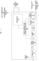
- FIG. 1 depicts an example embodiment of an optical communication system, including a transmitter and a receiver, which is configured to support clock recovery and polarization tracking based on a set of pilot optical frequency lines provided from the transmitter to the receiver.
- the optical communication system 100 includes a transmitter 110, a receiver 120, and a communication channel 130.
- the transmitter 110 transmits data 101 to the receiver 120 via the communication channel 130.
- the receiver 120 receives the data 101 from the transmitter 110 via the communication channel 130.
- the optical communication system 100 may be used for various types of optical communication channels which may be used as the communication channel 130, such as point-to-point fiber links, point to multi-point (P2MP) fiber links, free-space optical channels, and so forth.
- the transmitter 110 is configured to transmit the data 101 to the receiver 120 via the communication channel 130.
- the transmitter 110 includes a signal generation subsystem 111, a set of transmitter subsystems 115-1 to 115-N (collectively, transmitter subsystems 115), and a multiplexer 118. It will be appreciated that the transmitter 110 may include various other elements.
- the signal generation subsystem 111 outputs two pilot optical frequency lines 112-C1 and 112-C2 (collectively, pilot optical frequency lines 112, which also may be referred to more simply using the designators C1 and C2) and a transmitter clock 113.
- the two pilot optical frequency lines 112 are provided to the multiplexer 118 for transmission downstream toward the receiver 120.
- the transmitter clock 113 is provided to each of the N synchronized transmitter subsystems 115.
- the signal generation subsystem 111 optionally may generate a set of optical carrier signals 114-1 to 114-N (collectively, optical carrier signals 114, which also may be referred to as optical carrier frequencies f 1 - f N and referenced more generally as optical carrier frequencies f k ), which may be modulated by the data 101 for transmission of the data 101 toward the receiver 120.
- optical carrier signals 114 which also may be referred to as optical carrier frequencies f 1 - f N and referenced more generally as optical carrier frequencies f k , which may be modulated by the data 101 for transmission of the data 101 toward the receiver 120.
- N optical carrier signals 114 may be generated if each of the N transmitter subsystems 115 uses coherent homodyne detection (i.e., a 1:1 mapping between the optical carrier signals 114 and the transmitter subsystems 115), whereas fewer optical carrier signals 114 (e.g., between 0 and N-1) may be generated and used where any of the N transmitter subsystems 115 supports other than coherent homodyne detection (e.g., direct modulation, coherent intradyne detection, coherent heterodyne, or the like, as well as various combinations thereof).
- coherent homodyne detection i.e., a 1:1 mapping between the optical carrier signals 114 and the transmitter subsystems 115
- fewer optical carrier signals 114 e.g., between 0 and N-1
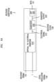
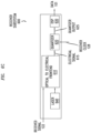
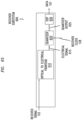
- the signal generation subsystem 111 may be implemented as presented with respect to FIG. 2 , FIG. 3 , or FIG. 4 .
- the transmitter subsystems 115 receive the data 101 and generate downstream data signals 117-1 to 117-N (collectively, downstream data signals 117) which are provided to the multiplexer 118 for transmission downstream toward the receiver 120.
- the transmitter subsystems 115 when the signal generation subsystem 111 generates the optical carrier signals 114, may modulate the optical carrier signals 114 by the data 101 to generate the downstream data signals 117.
- the downstream data signals 117 may be single-polarization signals or dual-polarization signals (having associated polarization states that may need to be aligned, as discussed further below).
- the transmitter subsystem 115 may be implemented as presented with respect to FIGs. 5A-5D .
- the multiplexer 118 multiplexes the pilot optical frequency lines 112 and the downstream data signals 117 to form a multiplexed downstream signal 131 that is propagated to the receiver 120 via the communication channel 130. It is noted that the multiplexing of the downstream data signals 117 may be performed in a manner such that the polarization states of the downstream data signals 117 are aligned to each other.
- optical carrier signals 114 may depend on whether or not homodyne operation is performed at the receiver 120 (in general, use of such optical carrier signals 114 may be beneficial if coherent detection is performed on the receiver side, as it allows a reduction of the required receiver bandwidth and enables symbol rate sampling with minimum penalty but is not required for a generic coherent intradyne detection with oversampling, or for direct detection).
- the receiver 120 is configured to receiver the data 101 from the transmitter 110 via the communication channel 130.
- the receiver 120 includes a polarization controller 121, an optical splitter 123, a set of receiver subsystems 125-1 to 125-k (collectively, receiver subsystems 125), and a clock synchronization and polarization tracking subsystem 126. It will be appreciated that the receiver 120 may include various other elements.
- the polarization controller 121 receives the multiplexed downstream signal 131' from the transmitter 110 via the communication channel 130.
- the polarization controller 121 aligns the polarization state at the receiver input based on a polarization control feedback signal 127 from the clock synchronization and polarization tracking subsystem 126.
- the polarization controller 121 provides the received signal 122, which includes the pilot optical frequency lines 112' and the downstream data signals 117', to the optical splitter 123.
- the optical splitter 123 is a (k+1) optical splitter that splits the received signal 122 into k+1 branches, which are provided to the k receiver subsystems 125 and the clock synchronization and polarization tracking subsystem 126, respectively.
- the receiver subsystems 125 are configured to receive the received signal 122 and recover the data 101 from the received signal 122 based on clock synchronization and polarization tracking functions performed by the clock synchronization and polarization tracking subsystem 126.
- the receiver subsystems 125 are configured to receive a receiver clock 128 from the clock synchronization and polarization tracking subsystem 126 and use the receiver clock 128 to recover the data 101 from the received signal 122.
- the receiver subsystems 125 in the case of homodyne detection, also may receive a set of local oscillator signals 129-1 to 129-P (collectively, local oscillator signals 129, which also may be referred to as optical frequencies f' 1 - f' P and referenced more generally as optical frequencies f' k , where P may or may not be equal to N, which are analogous to the optical carrier signals 114-1 to 114-N (optical carrier frequencies f k ) at the transmitter 110), which may be used as external local oscillator inputs for the receiver subsystems 125, respectively.
- local oscillator signals 129 which also may be referred to as optical frequencies f' 1 - f' P and referenced more generally as optical frequencies f' k , where P may or may not be equal to N, which are analogous to the optical carrier signals 114-1 to 114-N (optical carrier frequencies f k ) at the transmitter 110), which may be used as external local oscillator inputs for the
- the local oscillator signals 129 may be obtained from a regenerated OFC which may be regenerated at the receiver 120 (e.g., based on pilot optical frequency lines 112' received from the transmitter 110). It is noted that, in at least some example embodiments, a receiver subsystem 125 may be implemented as presented with respect to FIGs. 6A-6D .
- the clock synchronization and polarization tracking subsystem 126 is configured to receive the received signal 122 and generate the polarization control feedback signal 127, the receiver clock 128, and, optionally, the local oscillator signals 129.
- the clock synchronization and polarization tracking subsystem 126 is configured to generate the polarization control feedback signal 127 and the receiver clock 128, as well as the local oscillator signals 129 when used, based on the pilot optical frequency lines 112' which are included in the received signal 122.
- the two pilot optical frequency lines 112' and the local oscillator signals 129 may be referred to more generally as optical frequency lines or equally-spaced correlated optical frequency lines (where such equally-spaced correlated optical frequency lines may be based on regeneration of an OFC at the receiver 120 based on two pilot optical frequency lines 112' or may be based on one or more other suitable sources of equally-spaced correlated optical frequency lines at the receiver 120).
- the clock synchronization and polarization tracking subsystem 126 provides the polarization control feedback signal 127 to the polarization controller 121 for use by the polarization controller 121 in aligning the polarization state.
- the clock synchronization and polarization tracking subsystem 126 provides the receiver clock 128 to each of the receiver subsystems 129 for use by the receiver subsystems 129 to synchronize the receiver clock and processing with the transmitter clock 113 used at the transmitter 110. In this manner, clock synchronization and polarization tracking is achieved based on the two pilot optical frequency lines 112' provided from the transmitter 110 to the receiver 120. It is noted that, in at least some example embodiments, clock synchronization and polarization tracking subsystem 126 may be implemented as presented with respect to FIG. 7 or FIG. 8 .
- the required photoreceiver bandwidth can be lowered due to absence of frequency offset and symbol rate sampling can be enabled allowing for DSP-free coherent reception (e.g., while some DSP steps may be necessary depending on the wavelength/fiber distance/modulation format, in principle a simple modulation format such as quadrature phase shift keying (QPSK) over a typical PON distance of 20 km could be received DSP-free).
- QPSK quadrature phase shift keying
- the set of pilot optical frequency lines that is used for clock synchronization, polarization tracking, and homodyne coherent detection may include more than two optical frequency lines.
- wavelength-tunable receiver subsystems based on use of optical splitters and tunable local oscillators
- various example embodiments may be configured to use wavelength demultiplexers and/or splitter/filter structures (e.g., in various contexts, including for direct detection).
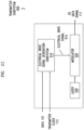
- FIG. 2 depicts an example embodiment of a signal generation subsystem for use in the transmitter of the optical communication system of FIG. 1 .
- the signal generation subsystem 200 may be used as the signal generation subsystem 111 of FIG. 1 (with FIG. 2 illustrating configuration of the signal generation subsystem 200 to output the two pilot optical frequency lines 112 (C1 and C2), the transmitter clock 113, and, optionally, the optical carrier signals 114 (denoted using optical carrier frequencies f 1 - f N )).
- the transmitter clock 113 and the spacing of the optical frequency lines are both derived from a reference clock (e.g., a system clock, a clock derived from a system clock, or the like).
- a reference clock e.g., a system clock, a clock derived from a system clock, or the like.
- the signal generation subsystem 200 may include a reference clock 210, an optical frequency line subsystem 220, and a demultiplexer 230.
- the signal generation subsystem 200 may generate the transmitter clock 113, the pilot optical frequency lines 112, and the optical carrier signals 114 based on the reference clock 210.
- the reference clock 210 is converted by a clock converter 211 based on a conversion factor (indicated by ⁇ , where ⁇ is a rational number, which may indicate multiplication or division in accordance with the conversion factor) ) to provide a converted clock to drive the optical frequency line subsystem 220 which generates the pilot optical frequency lines 112 and the optical carrier signals 114.
- the reference clock 210 is converted by a clock converter 212 based on a conversion factor (indicated by ⁇ , where ⁇ is a rational number, which may indicate multiplication or division in accordance with the conversion factor) to produce the transmitter clock 113.
- a conversion factor indicated by ⁇ , where ⁇ is a rational number, which may indicate multiplication or division in accordance with the conversion factor
Landscapes
- Engineering & Computer Science (AREA)
- Computer Networks & Wireless Communication (AREA)
- Signal Processing (AREA)
- Physics & Mathematics (AREA)
- Optics & Photonics (AREA)
- Electromagnetism (AREA)
- Optical Communication System (AREA)
Applications Claiming Priority (1)
| Application Number | Priority Date | Filing Date | Title |
|---|---|---|---|
| US18/469,524 US12519607B2 (en) | 2023-09-18 | 2023-09-18 | Clock synchronization and polarization tracking in optical communication systems |
Publications (1)
| Publication Number | Publication Date |
|---|---|
| EP4525329A1 true EP4525329A1 (de) | 2025-03-19 |
Family
ID=92843352
Family Applications (1)
| Application Number | Title | Priority Date | Filing Date |
|---|---|---|---|
| EP24200978.5A Pending EP4525329A1 (de) | 2023-09-18 | 2024-09-18 | Taktsynchronisierung und polarisationsnachführung in optischen kommunikationssystemen |
Country Status (2)
| Country | Link |
|---|---|
| US (1) | US12519607B2 (de) |
| EP (1) | EP4525329A1 (de) |
Families Citing this family (1)
| Publication number | Priority date | Publication date | Assignee | Title |
|---|---|---|---|---|
| US12494954B1 (en) * | 2024-06-06 | 2025-12-09 | National Tsing Hua University | Decoder for decoding data in a PAM-(2M+1-1) format because of 1+D pulse shaping, decoder device using the decoder, and receiver using the decoder device |
Citations (3)
| Publication number | Priority date | Publication date | Assignee | Title |
|---|---|---|---|---|
| US20040067063A1 (en) * | 2002-10-08 | 2004-04-08 | Jae-Myoung Lee | Method and apparatus of clock recovery using optical filters |
| WO2018198873A1 (ja) * | 2017-04-28 | 2018-11-01 | 国立大学法人東北大学 | 光伝送方法および光伝送装置 |
| US20220085886A1 (en) * | 2020-09-15 | 2022-03-17 | California Institute Of Technology | Optically enabled rf phased-arrays for data transmission |
Family Cites Families (8)
| Publication number | Priority date | Publication date | Assignee | Title |
|---|---|---|---|---|
| JP3950899B2 (ja) * | 2005-08-03 | 2007-08-01 | 株式会社日立コミュニケーションテクノロジー | ビット同期回路 |
| US7519750B2 (en) * | 2006-07-18 | 2009-04-14 | Cortina Systems, Inc. | Linear burst mode synchronizer for passive optical networks |
| JP5111092B2 (ja) * | 2007-12-21 | 2012-12-26 | 株式会社日立製作所 | ネットワークシステム及びolt |
| US8670439B2 (en) * | 2010-07-02 | 2014-03-11 | Futurewei Technologies, Inc. | Method for accurate distribution of time to a receiver node in an access network |
| EP2919400A1 (de) * | 2014-03-13 | 2015-09-16 | Alcatel Lucent | Verfahren und Vorrichtung zur Weiterleitung einer Taktsynchronisierungsnachricht |
| US10305621B2 (en) * | 2016-07-26 | 2019-05-28 | Futurewei Technologies, Inc. | Burst-mode discrete multi-tone for networks |
| JP6988604B2 (ja) * | 2018-03-16 | 2022-01-05 | 日本電信電話株式会社 | 光変復調方法、光通信システム、光送信装置及び光受信装置 |
| US11265099B1 (en) * | 2019-05-17 | 2022-03-01 | Cable Television Laboratories, Inc. | System and methods for time and frequency division passive optical network |
-
2023
- 2023-09-18 US US18/469,524 patent/US12519607B2/en active Active
-
2024
- 2024-09-18 EP EP24200978.5A patent/EP4525329A1/de active Pending
Patent Citations (3)
| Publication number | Priority date | Publication date | Assignee | Title |
|---|---|---|---|---|
| US20040067063A1 (en) * | 2002-10-08 | 2004-04-08 | Jae-Myoung Lee | Method and apparatus of clock recovery using optical filters |
| WO2018198873A1 (ja) * | 2017-04-28 | 2018-11-01 | 国立大学法人東北大学 | 光伝送方法および光伝送装置 |
| US20220085886A1 (en) * | 2020-09-15 | 2022-03-17 | California Institute Of Technology | Optically enabled rf phased-arrays for data transmission |
Non-Patent Citations (1)
| Title |
|---|
| LEE J ET AL: "Enhancement of clock component in a nonreturn-to-zero signal through beating process", OPTICAL FIBER TECHNOLOGY, ELSEVIER, AMSTERDAM, NL, vol. 12, no. 1, 1 January 2006 (2006-01-01), pages 59 - 70, XP024917304, ISSN: 1068-5200, [retrieved on 20060101], DOI: 10.1016/J.YOFTE.2005.06.001 * |
Also Published As
| Publication number | Publication date |
|---|---|
| US20250097002A1 (en) | 2025-03-20 |
| US12519607B2 (en) | 2026-01-06 |
Similar Documents
| Publication | Publication Date | Title |
|---|---|---|
| Shahpari et al. | Coherent access: A review | |
| EP2420011B1 (de) | Verfahren und system zum detektieren von versatz zwischen parallelen signalen | |
| CN105099570B (zh) | 正交多载波光源及pdm-qpsk信号发射装置 | |
| EP2559173B1 (de) | Verfahren und vorrichtung für die übertragung und den empfang eines optischen multiplex-polarisationssignals | |
| US8594515B2 (en) | Digital phase conjugation for fiber-optic links | |
| US11387929B1 (en) | Systems and methods for carrier phase recovery | |
| US8184973B2 (en) | Direct detection for receiving polarization multiplexing signals | |
| EP2482486B1 (de) | Abtasttaktsynchronisierungsvorrichtung, digitale kohärente Empfangsvorrichtung und Abtasttaktsynchronisierungsverfahren | |
| CN102761373A (zh) | 一种实现相干接收的高速大容量无源光网络系统及方法 | |
| WO2013039960A1 (en) | Interferometer configured for signal processing in an interference path | |
| JP5068240B2 (ja) | 光伝送方式、送信器及び受信器 | |
| WO2012003856A1 (en) | Method and device for data processing in an optical communication network | |
| EP4525329A1 (de) | Taktsynchronisierung und polarisationsnachführung in optischen kommunikationssystemen | |
| EP2204928B1 (de) | Verfahren und Vorrichtung zum Empfang eines OPFDM-DQPSK-Signals | |
| US20120263468A1 (en) | Generation of Optical Quadrature Duobinary Format Using Optical Delay | |
| Huang et al. | Transmission of spectral efficient super-channels using all-optical OFDM and digital coherent receiver technologies | |
| Da Silva et al. | Combined optical and electrical spectrum shaping for high-baud-rate nyquist-WDM transceivers | |
| US20250184010A1 (en) | System and method for optical communication | |
| JP4802270B2 (ja) | 光位相変調方式における光位相同期方法および光位相同期装置 | |
| Freund et al. | Single-and multi-carrier techniques to build up Tb/s per channel transmission systems | |
| Mahdiraji et al. | Advanced modulation formats and multiplexing techniques for optical telecommunication systems | |
| WO2012032130A1 (en) | Multi-carrier system and method for use in an optical network | |
| Olsson et al. | Electro-optical subcarrier modulation transmitter for 100 GbE DWDM transport | |
| Mazur et al. | Joint superchannel digital signal processing for ultimate bandwidth utilization | |
| US12580663B2 (en) | Coherent detection of subcarrier-multiplexed signals using a frequency comb |
Legal Events
| Date | Code | Title | Description |
|---|---|---|---|
| PUAI | Public reference made under article 153(3) epc to a published international application that has entered the european phase |
Free format text: ORIGINAL CODE: 0009012 |
|
| STAA | Information on the status of an ep patent application or granted ep patent |
Free format text: STATUS: THE APPLICATION HAS BEEN PUBLISHED |
|
| AK | Designated contracting states |
Kind code of ref document: A1 Designated state(s): AL AT BE BG CH CY CZ DE DK EE ES FI FR GB GR HR HU IE IS IT LI LT LU LV MC ME MK MT NL NO PL PT RO RS SE SI SK SM TR |
|
| STAA | Information on the status of an ep patent application or granted ep patent |
Free format text: STATUS: REQUEST FOR EXAMINATION WAS MADE |
|
| 17P | Request for examination filed |
Effective date: 20250919 |