EP4525574A1 - Ensemble de connexion et appareil électronique le comprenant - Google Patents
Ensemble de connexion et appareil électronique le comprenant Download PDFInfo
- Publication number
- EP4525574A1 EP4525574A1 EP24195607.7A EP24195607A EP4525574A1 EP 4525574 A1 EP4525574 A1 EP 4525574A1 EP 24195607 A EP24195607 A EP 24195607A EP 4525574 A1 EP4525574 A1 EP 4525574A1
- Authority
- EP
- European Patent Office
- Prior art keywords
- component
- engaging portion
- heat dissipating
- dissipating fins
- along
- Prior art date
- Legal status (The legal status is an assumption and is not a legal conclusion. Google has not performed a legal analysis and makes no representation as to the accuracy of the status listed.)
- Granted
Links
Images





Classifications
-
- H—ELECTRICITY
- H01—ELECTRIC ELEMENTS
- H01R—ELECTRICALLY-CONDUCTIVE CONNECTIONS; STRUCTURAL ASSOCIATIONS OF A PLURALITY OF MUTUALLY-INSULATED ELECTRICAL CONNECTING ELEMENTS; COUPLING DEVICES; CURRENT COLLECTORS
- H01R13/00—Details of coupling devices of the kinds covered by groups H01R12/70 or H01R24/00 - H01R33/00
- H01R13/64—Means for preventing incorrect coupling
- H01R13/642—Means for preventing incorrect coupling by position or shape of contact members
-
- H—ELECTRICITY
- H05—ELECTRIC TECHNIQUES NOT OTHERWISE PROVIDED FOR
- H05K—PRINTED CIRCUITS; CASINGS OR CONSTRUCTIONAL DETAILS OF ELECTRIC APPARATUS; MANUFACTURE OF ASSEMBLAGES OF ELECTRICAL COMPONENTS
- H05K5/00—Casings, cabinets or drawers for electric apparatus
- H05K5/02—Details
- H05K5/0217—Mechanical details of casings
-
- H—ELECTRICITY
- H01—ELECTRIC ELEMENTS
- H01R—ELECTRICALLY-CONDUCTIVE CONNECTIONS; STRUCTURAL ASSOCIATIONS OF A PLURALITY OF MUTUALLY-INSULATED ELECTRICAL CONNECTING ELEMENTS; COUPLING DEVICES; CURRENT COLLECTORS
- H01R13/00—Details of coupling devices of the kinds covered by groups H01R12/70 or H01R24/00 - H01R33/00
- H01R13/46—Bases; Cases
- H01R13/52—Dustproof, splashproof, drip-proof, waterproof, or flameproof cases
- H01R13/521—Sealing between contact members and housing, e.g. sealing insert
-
- H—ELECTRICITY
- H01—ELECTRIC ELEMENTS
- H01R—ELECTRICALLY-CONDUCTIVE CONNECTIONS; STRUCTURAL ASSOCIATIONS OF A PLURALITY OF MUTUALLY-INSULATED ELECTRICAL CONNECTING ELEMENTS; COUPLING DEVICES; CURRENT COLLECTORS
- H01R13/00—Details of coupling devices of the kinds covered by groups H01R12/70 or H01R24/00 - H01R33/00
- H01R13/62—Means for facilitating engagement or disengagement of coupling parts or for holding them in engagement
- H01R13/629—Additional means for facilitating engagement or disengagement of coupling parts, e.g. aligning or guiding means, levers, gas pressure electrical locking indicators, manufacturing tolerances
- H01R13/62905—Additional means for facilitating engagement or disengagement of coupling parts, e.g. aligning or guiding means, levers, gas pressure electrical locking indicators, manufacturing tolerances comprising a camming member
- H01R13/62927—Comprising supplementary or additional locking means
-
- H—ELECTRICITY
- H05—ELECTRIC TECHNIQUES NOT OTHERWISE PROVIDED FOR
- H05K—PRINTED CIRCUITS; CASINGS OR CONSTRUCTIONAL DETAILS OF ELECTRIC APPARATUS; MANUFACTURE OF ASSEMBLAGES OF ELECTRICAL COMPONENTS
- H05K5/00—Casings, cabinets or drawers for electric apparatus
- H05K5/06—Hermetically-sealed casings
-
- H—ELECTRICITY
- H05—ELECTRIC TECHNIQUES NOT OTHERWISE PROVIDED FOR
- H05K—PRINTED CIRCUITS; CASINGS OR CONSTRUCTIONAL DETAILS OF ELECTRIC APPARATUS; MANUFACTURE OF ASSEMBLAGES OF ELECTRICAL COMPONENTS
- H05K7/00—Constructional details common to different types of electric apparatus
- H05K7/14—Mounting supporting structure in casing or on frame or rack
- H05K7/1422—Printed circuit boards receptacles, e.g. stacked structures, electronic circuit modules or box like frames
- H05K7/1435—Expandable constructions
-
- H—ELECTRICITY
- H05—ELECTRIC TECHNIQUES NOT OTHERWISE PROVIDED FOR
- H05K—PRINTED CIRCUITS; CASINGS OR CONSTRUCTIONAL DETAILS OF ELECTRIC APPARATUS; MANUFACTURE OF ASSEMBLAGES OF ELECTRICAL COMPONENTS
- H05K7/00—Constructional details common to different types of electric apparatus
- H05K7/20—Modifications to facilitate cooling, ventilating, or heating
- H05K7/2039—Modifications to facilitate cooling, ventilating, or heating characterised by the heat transfer by conduction from the heat generating element to a dissipating body
-
- H—ELECTRICITY
- H05—ELECTRIC TECHNIQUES NOT OTHERWISE PROVIDED FOR
- H05K—PRINTED CIRCUITS; CASINGS OR CONSTRUCTIONAL DETAILS OF ELECTRIC APPARATUS; MANUFACTURE OF ASSEMBLAGES OF ELECTRICAL COMPONENTS
- H05K7/00—Constructional details common to different types of electric apparatus
- H05K7/20—Modifications to facilitate cooling, ventilating, or heating
- H05K7/2039—Modifications to facilitate cooling, ventilating, or heating characterised by the heat transfer by conduction from the heat generating element to a dissipating body
- H05K7/20409—Outer radiating structures on heat dissipating housings, e.g. fins integrated with the housing
-
- H—ELECTRICITY
- H01—ELECTRIC ELEMENTS
- H01R—ELECTRICALLY-CONDUCTIVE CONNECTIONS; STRUCTURAL ASSOCIATIONS OF A PLURALITY OF MUTUALLY-INSULATED ELECTRICAL CONNECTING ELEMENTS; COUPLING DEVICES; CURRENT COLLECTORS
- H01R24/00—Two-part coupling devices, or either of their cooperating parts, characterised by their overall structure
- H01R24/60—Contacts spaced along planar side wall transverse to longitudinal axis of engagement
Definitions
- the present invention relates to a connecting assembly and an electronic apparatus according to the pre-characterizing clauses of claims 1 and 11.
- the electronic apparatus usually includes multiple detachable devices structurally and electrically connected to each other.
- the detachable device can be a power supply device, a signal switch device, or a computing device. Therefore, it is an important topic in the field to provide a tight and firm aligning connection between the two detachable devices for improving a reliability of the electronic apparatus.
- the present invention aims at providing a connecting assembly for providing an aligning connection between a first electronic device and a second electronic device tightly and firmly, and an electronic apparatus therewith.
- the claimed connecting assembly for aligning and connecting a first electronic device and a second electronic device includes a first connecting component, a plurality of first heat dissipating fins, a second connecting component, a plurality of second heat dissipating fins, and a pin protruding.
- the first connecting component is disposed on the first electronic device.
- the plurality of first heat dissipating fins are disposed on the first connecting component.
- An engaging portion is formed on at least one of the plurality of first heat dissipating fins.
- the second connecting component is disposed on the second electronic device.
- the plurality of second heat dissipating fins are disposed on the second connecting component.
- a cooperating engaging portion is formed on at least one of the plurality of second heat dissipating fins.
- the pin protrudes from the first connecting component and configured to be inserted into the second connecting component along a first direction.
- the plurality of first heat dissipating fins are configured to respectively be aligned with and abut against the plurality of second heat dissipating fins along the first direction
- the engaging portion is configured to engage with the cooperating engaging portion along the first direction and abut against the cooperating engaging portion along a second direction and a third direction opposite to each other and perpendicular to the first direction.
- the claimed electronic apparatus includes a first electronic device, a second electronic device detachably connected to the first electronic device, and the aforementioned connecting assembly for providing an aligning connection between the first electronic device and the second electronic device.
- a cooperation of the engaging portion and the cooperating engaging portion can provide support for the pin along a vertical direction relative to the pin for reducing a vertical shear force acting on the pin, so as to prevent the pin from being damaged or broken.
- the cooperation of the engaging portion and the cooperating engaging portion also can ensure the first electronic device and the second electronic device to be connected to each other and prevent the first electronic device or the second electronic device from being connected to another electronic device by mistake, so as to achieve a foolproof effect. From the above, the present invention has improved reliability in use.
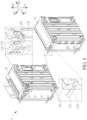
- FIG. 1 is a schematic diagram of an electronic apparatus 1 according to an embodiment of the present invention.
- FIG. 2 and FIG. 3 are exploded diagrams of the electronic apparatus 1 at different views according to the embodiment of the present invention.
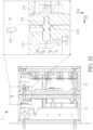
- FIG. 4 to FIG. 7 are partial sectional diagrams of the electronic apparatus 1 along different sectional lines according to the embodiment of the present invention.
- the electronic apparatus 1 includes a first electronic device 11 and a second electronic device 12.
- the second electronic device 12 is detachably connected to the first electronic device 11.
- the electronic apparatus 1 can be a remote terminal unit, and the first electronic device 11 and the second electronic device 12 can be a signal switch device and a radio frequency (RF) communication device, respectively.
- RF radio frequency
- the electronic apparatus 1 further includes a connecting assembly 13 configured to provide a tight and firm aligning connection between the first electronic device 11 and the second electronic device 12.
- the connecting assembly 13 includes a first connecting component 131, a second connecting component 132, four pins 133, six first heat dissipating fins 13A and six second heat dissipating fins 13B.
- the first connecting component 131 is disposed on the first electronic device 11.
- the second connecting component 132 is disposed on the second electronic device 12.
- Each of the pins 133 protrudes from the first connecting component 131 and is configured to be inserted into the second connecting component 132 along a first direction D1.
- the four pins 133 are located on four corners of the first connecting component 131, respectively.
- the six first heat dissipating fins 13A are disposed on the first connecting component 131 and configured to dissipate heat generated by the first electronic device 11 rapidly.
- the six second heat dissipating fins 13B are disposed on the second connecting component 132 and configured to dissipate heat generated by the second electronic device 12 rapidly.
- Two engaging portions 13A1 are formed on each of four of the six first heat dissipating fins 13A.
- Two cooperating engaging portions 13B1 are formed on each of four of the six second heat dissipating fins 13B.
- each of the pins 133 When each of the pins 133 is inserted into the second connecting component 132 along the first direction D1, the six first heat dissipating fins 13A are configured to be aligned with and abut against the six second heat dissipating fins 13B, respectively, and each of the engaging portions 13A1 is configured to engage with the corresponding cooperating engaging portion 13B1 along the first direction D1 and abut against the corresponding cooperating engaging portion 13B1 along a second direction D2 and a third direction D3 opposite to each other and perpendicular to the first direction D 1.
- each of the engaging portions 13A1 and the corresponding cooperating engaging portion 13B1 can provide support for the pin 133 along a vertical direction relative to the pin 133 for reducing a vertical shear force acting on the pin 133, so as to prevent the pin 133 from being damaged or broken.
- the abutting cooperation of each of the engaging portions 13A1 and the corresponding cooperating engaging portion 13B1 also can ensure the first electronic device 11 and the second electronic device 12 to be connected to each other and prevent the first electronic device 11 or the second electronic device 12 from being connected to another electronic device by mistake, so as to achieve a foolproof effect.
- the numbers of the pin, the first heat dissipating fin, the second heat dissipating fin, the engaging portion and the cooperating engaging portion are not limited to this embodiment.
- the connecting assembly can include one pin, two first heat dissipating fins and two second heat dissipating fins, and one engaging portion and one cooperating engaging portion are formed on one of the two first heat dissipating fins and one of the two second heat dissipating fins, respectively.
- the first connecting component 131 can be integrally connected to a left cover of the first electronic device 11, and the second connecting component 132 can be integrally connected to a right cover of the second electronic device 12.
- the present invention is not limited to this embodiment.
- the first connecting component can be an independent member detachably connected to the left cover of the first electronic device
- the second connecting component can be an independent member detachably connected to the right cover of the second electronic device.
- the first heat dissipating fins 13A can be integrally connected to the first connecting component 131, and the second heat dissipating fins 13B can be integrally connected to the second connecting component 132.
- the present invention is not limited to this embodiment.
- the first heat dissipating fins can be an independent member detachably connected to the first connecting component, and the second heat dissipating fins can be an independent member detachably connected to the second connecting component.
- the engaging portion 13A1 and the cooperating engaging portion 13B1 can be an engaging protrusion and an engaging recess.
- a width of the engaging protrusion can gradually decrease from a bottom of the engaging protrusion, and a width of the engaging recess can gradually increase from a bottom of the engaging recess.
- the engaging protrusion can be a trapezoid-shaped protrusion with a width gradually decreasing along the first direction D1
- the engaging recess can be a trapezoid-shaped recess with a width gradually decreasing along the first direction D1.
- Such configuration guides the engaging portion 13A1 and the cooperating engaging portion 13B1 to be aligned with each other by a sliding cooperation between corresponding inclined surfaces thereof during a process of that the first electronic device 11 and the second electronic device 12 move toward each other.
- the engaging portion and the cooperating engaging portion can be an engaging recess and an engaging protrusion, and the engaging portion and the cooperating engaging portion have substantially uniform widths, i.e., the engaging portion and the cooperating engaging portion can be a rectangular recess and a rectangular protrusion, respectively.
- a first one, a second one, a third one, a fourth one, a fifth one and a sixth one of the six first heat dissipating fins 13A can be sequentially arranged along a fourth direction D4, and the engaging portions 13A1 on the first one, the second one, the fourth one and the sixth one of the six first heat dissipating fins 13A can be considered as two first engaging portions 13A11, two second engaging portions 13A12, two third engaging portions 13A13 and two fourth engaging portions 13A14, respectively.
- the second one of the six first heat dissipating fins 13A, whereon the second engaging portions 13A12 are formed, is located between the first one and the fourth one of the six first heat dissipating fins 13A, whereon the first engaging portions 13A11 and the third engaging portions 13A13 are respectively formed, along the fourth direction D4.
- Each of the second engaging portions 13A12 and the corresponding first engaging portion 13A11 are misaligned from each other along the fourth direction D4.
- Each of the second engaging portions 13A12 and the corresponding third engaging portion 13A13 are misaligned from each other along the fourth direction D4.
- the fourth one of the six first heat dissipating fins 13A, whereon the third engaging portions 13A13 are formed, is located between the second one and the sixth one of the six first heat dissipating fins 13A, whereon the second engaging portions 13A12 and the fourth engaging portions 13A14 are respectively formed, along the fourth direction D4.
- Each of the third engaging portions 13A13 and the corresponding second engaging portion 13A12 are misaligned from each other along the fourth direction D4.
- Each of the third engaging portions 13A13 and the corresponding fourth engaging portion 13A14 are misaligned from each other along the fourth direction D4.
- a first one, a second one, a third one, a fourth one, a fifth one and a sixth one of the six second heat dissipating fins 13B can be sequentially arranged along the fourth direction D4, and the cooperating engaging portions 13B1 on the first one, the second one, the fourth one and the sixth one of the six second heat dissipating fins 13B can be considered as two first cooperating engaging portions 13B11, two second cooperating engaging portions 13B12, two third cooperating engaging portions 13B13 and two fourth cooperating engaging portions 13B14.
- the second one of the six second heat dissipating fins 13B, whereon the second cooperating engaging portions 13B 12 are formed, is located between the first one and the fourth one of the six second heat dissipating fins 13B, whereon the first cooperating engaging portions 13B11 and the third cooperating engaging portions 13B13 are respectively formed, along the fourth direction D4.
- Each of the second cooperating engaging portions 13B12 and the corresponding first cooperating engaging portion 13B11 are misaligned from each other along the fourth direction D4.
- Each of the second cooperating engaging portions 13B12 and the corresponding third cooperating engaging portion 13B13 are misaligned from each other along the fourth direction D4.
- the fourth one of the six second heat dissipating fins 13B, whereon the third cooperating engaging portions 13B13 are formed, is located between the second one and the sixth one of the six second heat dissipating fins 13B, whereon the second cooperating engaging portions 13B12 and the fourth cooperating engaging portions 13B14 are respectively formed, along the fourth direction D4.
- Each of the third cooperating engaging portions 13B13 and the corresponding second cooperating engaging portion 13B12 are misaligned from each other along the fourth direction D4.
- Each of the third cooperating engaging portions 13B13 and the corresponding fourth cooperating engaging portion 13B14 are misaligned from each other along the fourth direction D4.
- FIG. 8 is a partial sectional exploded diagram of the electronic apparatus 1 according to the embodiment of the present invention.
- FIG. 9 is a partial structural diagram of the electronic apparatus 1 in a non-locked state according to the embodiment of the present invention.
- FIG. 10 and FIG. 11 are partial sectional diagrams of the electronic apparatus 1 in the non-locked state along different sectional lines according to the embodiment of the present invention.
- FIG. 12 is a partial structural diagram of the electronic apparatus 1 in a locked state according to the embodiment of the present invention.
- FIG. 13 and FIG. 14 are partial sectional diagrams of the electronic apparatus 1 in the locked state along different sectional lines according to the embodiment of the present invention. As shown in FIG. 2 , FIG.
- the connecting assembly 13 further includes four resilient components 134, four locking components 135 and four abutting components 136.
- Each of the resilient components 134 is disposed inside the second connecting component 132 and configured to apply a radial resilient force onto the corresponding pin 133 inserted into the second connecting component 132.
- Each of the locking components 135 is screwed onto the second connecting component 132 and configured to apply a radial locking force onto the corresponding pin 133 inserted into the second connecting component 132.
- Each of the abutting components 136 is disposed inside the second connecting component 132 and configured to abut against the corresponding pin 133.
- the resilient component 134 is configured to abut against the abutting component 136 to indirectly apply the radial resilient force onto the pin 133 via the abutting component 136.
- the resilient component 134 is configured to apply the radial resilient force onto the corresponding pin 133 inserted into the second connecting component 132 along a first forcing direction F1
- the locking components 135 is configured to apply the radial locking force onto the corresponding pin 133 inserted into the second connecting component 132 along a second forcing direction F2, wherein the first forcing direction F1 and the second forcing direction F2 can be substantially perpendicular to each other and substantially perpendicular to the first direction D1, and first forcing direction F1 and the second forcing direction F2 can be substantially opposite to the fourth direction D4 and the second direction D2, respectively.
- the locking component 135 can be a screw or a bolt
- the resilient component 134 can be a compression spring
- the abutting component 136 can be a ball-shaped structure made of metal material.
- the present invention is not limited to this embodiment.
- the abutting component can be a protruding platform made of plastic material or resilient material.
- the numbers of the pin, the resilient component and the locking component are not limited to this embodiment.
- the connecting assembly can include one pin, one resilient component and one locking component.
- the locking configuration for locking the pin is not limited to this embodiment.
- the abutting component can be omitted, and the resilient component can be a U-shaped spring configured to directly abut against two opposite sides of the pin to directly apply two radial resilient forces onto the pin along two opposite directions.
- a groove 1331 is formed on an outer periphery of each of the pins 133 along a circumferential direction of the corresponding pin 133 and configured to cooperate with the corresponding abutting component 136 and the corresponding locking component 135.
- Each of the grooves 1331 is abutted by the corresponding abutting component 136 along the first forcing direction F1 and the corresponding locking component 135 along the second forcing direction F2, so as to lock the corresponding pin 133 with the radial resilient force generated by the corresponding resilient component 134 along the first forcing direction F1 and the radial locking force generated by the corresponding locking component 135 along the second forcing direction F2 perpendicular to the first forcing direction F1.
- the connecting assembly 13 further includes a sealing component 137 disposed between the first connecting component 131 and the second connecting component 132.
- the sealing component 137 can be made of resilient material.
- the sealing component 137 can position the pin 133 at an initial inserting position as shown in FIG. 9 and FIG. 10 when the pin 133 is inserted to the second connecting component 132.
- a cooperation of the locking component 135 and the groove 1331 can drive the pin 133 to move from the initial inserting position P1 as shown in FIG. 9 and FIG. 10 to a predetermined inserting position P2 as shown in FIG. 12 and FIG.
- the aforementioned configuration achieves seamless connection of the first connecting component 131 and the second connecting component 132 to meet requirements of dustproof and waterproof functions for preventing moisture or particle from entering into the first electronic device 11 and/or the second electronic device 12.
- the sealing component 137 can be an O-shaped sealing ring surrounding an electrical connector of the first electronic device 11 and an electrical connector of the second electronic device 12.
- the present invention is not limited to this embodiment.
- the sealing component can be omitted.
- the pin can be configured to be located at the predetermined inserting position when being inserted into the second connecting component, and the locking component can be configured to lock the pin located at the predetermined inserting position after insertion of the pin into the second connecting component.
- a cooperation of the engaging portion and the cooperating engaging portion can provide support for the pin along a vertical direction relative to the pin for reducing a vertical shear force acting on the pin, so as to prevent the pin from being damaged or broken.
- the cooperation of the engaging portion and the cooperating engaging portion also can ensure the first electronic device and the second electronic device to be connected to each other and prevent the first electronic device or the second electronic device from being connected to another electronic device by mistake, so as to achieve a foolproof effect. From the above, the present invention has improved reliability in use.
Landscapes
- Engineering & Computer Science (AREA)
- Microelectronics & Electronic Packaging (AREA)
- Physics & Mathematics (AREA)
- Thermal Sciences (AREA)
- Cooling Or The Like Of Electrical Apparatus (AREA)
- Casings For Electric Apparatus (AREA)
- Connector Housings Or Holding Contact Members (AREA)
Applications Claiming Priority (2)
| Application Number | Priority Date | Filing Date | Title |
|---|---|---|---|
| US202363537201P | 2023-09-08 | 2023-09-08 | |
| TW113109745A TWI883868B (zh) | 2023-09-08 | 2024-03-15 | 連接組件以及具有前述連接組件的電子設備 |
Publications (2)
| Publication Number | Publication Date |
|---|---|
| EP4525574A1 true EP4525574A1 (fr) | 2025-03-19 |
| EP4525574B1 EP4525574B1 (fr) | 2025-12-10 |
Family
ID=92503759
Family Applications (1)
| Application Number | Title | Priority Date | Filing Date |
|---|---|---|---|
| EP24195607.7A Active EP4525574B1 (fr) | 2023-09-08 | 2024-08-21 | Ensemble de connexion et appareil électronique le comprenant |
Country Status (4)
| Country | Link |
|---|---|
| US (1) | US20250087942A1 (fr) |
| EP (1) | EP4525574B1 (fr) |
| JP (1) | JP7654928B2 (fr) |
| CN (1) | CN119603900A (fr) |
Citations (2)
| Publication number | Priority date | Publication date | Assignee | Title |
|---|---|---|---|---|
| US20050215107A1 (en) * | 2004-03-26 | 2005-09-29 | Castello Brian P | Guide receptacle with tandem mounting features |
| US20210100123A1 (en) * | 2017-12-22 | 2021-04-01 | Bull Sas | System and method for connecting at least one electronic card to a printed circuit board |
Family Cites Families (5)
| Publication number | Priority date | Publication date | Assignee | Title |
|---|---|---|---|---|
| US6009938A (en) * | 1997-12-11 | 2000-01-04 | Eastman Kodak Company | Extruded, tiered high fin density heat sinks and method of manufacture |
| JP2004158757A (ja) * | 2002-11-08 | 2004-06-03 | Omron Corp | 電子機器の放熱構造及びそれを用いたソリッドステートリレー |
| US20090165997A1 (en) * | 2007-12-27 | 2009-07-02 | Hon Hai Precision Industry Co., Ltd. | Heat sink |
| JP6645915B2 (ja) * | 2016-06-24 | 2020-02-14 | 三協立山株式会社 | ヒートシンク |
| JP6750584B2 (ja) * | 2017-08-30 | 2020-09-02 | 矢崎総業株式会社 | 車載機器の熱分散構造 |
-
2024
- 2024-04-03 CN CN202410403658.0A patent/CN119603900A/zh active Pending
- 2024-05-07 JP JP2024075049A patent/JP7654928B2/ja active Active
- 2024-07-22 US US18/780,445 patent/US20250087942A1/en active Pending
- 2024-08-21 EP EP24195607.7A patent/EP4525574B1/fr active Active
Patent Citations (2)
| Publication number | Priority date | Publication date | Assignee | Title |
|---|---|---|---|---|
| US20050215107A1 (en) * | 2004-03-26 | 2005-09-29 | Castello Brian P | Guide receptacle with tandem mounting features |
| US20210100123A1 (en) * | 2017-12-22 | 2021-04-01 | Bull Sas | System and method for connecting at least one electronic card to a printed circuit board |
Also Published As
| Publication number | Publication date |
|---|---|
| CN119603900A (zh) | 2025-03-11 |
| JP2025039513A (ja) | 2025-03-21 |
| US20250087942A1 (en) | 2025-03-13 |
| JP7654928B2 (ja) | 2025-04-02 |
| EP4525574B1 (fr) | 2025-12-10 |
Similar Documents
| Publication | Publication Date | Title |
|---|---|---|
| US5769668A (en) | Module alignment apparatus for an electrical connector | |
| US6482027B2 (en) | Electrical connector for flat cables | |
| US20170250483A1 (en) | Electrical connector and method of assembling the same | |
| US8727815B1 (en) | Compliant pin connector mounting system and method | |
| CN110556645A (zh) | 卡缘连接器组件 | |
| US6383010B1 (en) | Latching system for electrical connectors | |
| US10886640B2 (en) | Conductive terminal and electrical connector | |
| JP2002530822A (ja) | ガイド部材および取外しリセスを有する噛み合い電気コネクタアセンブリ | |
| US7108536B2 (en) | Socket connector having structure for preventing sideways movement | |
| CN212485679U (zh) | 浮动式导引插入连接器 | |
| US5487674A (en) | Surface mountable leaded package | |
| US6739880B2 (en) | Circuit board-to-board interconnection device | |
| EP4521862A1 (fr) | Ensemble de connexion et appareil électronique associé | |
| EP4525574B1 (fr) | Ensemble de connexion et appareil électronique le comprenant | |
| US5588862A (en) | Locking mechanism | |
| EP0214762A2 (fr) | Connecteur pour cassette avec mécanisme pivotant | |
| US20120040565A1 (en) | Co-edge connector | |
| US6319058B1 (en) | Pair of connectors clamping a printed circuit board | |
| US12476431B2 (en) | Bus bar assembly and floating connector thereof | |
| US5489219A (en) | Self-retaining board lock | |
| US6648700B1 (en) | Stepped/keying interface stabilization alignment mechanism | |
| US11631951B2 (en) | Plug electrical connector and receptacle electrical connector | |
| US5409393A (en) | Locking mechanism | |
| TWI883868B (zh) | 連接組件以及具有前述連接組件的電子設備 | |
| US6929496B2 (en) | Socket connector with actuator mechanism mating means |
Legal Events
| Date | Code | Title | Description |
|---|---|---|---|
| PUAI | Public reference made under article 153(3) epc to a published international application that has entered the european phase |
Free format text: ORIGINAL CODE: 0009012 |
|
| STAA | Information on the status of an ep patent application or granted ep patent |
Free format text: STATUS: THE APPLICATION HAS BEEN PUBLISHED |
|
| STAA | Information on the status of an ep patent application or granted ep patent |
Free format text: STATUS: REQUEST FOR EXAMINATION WAS MADE |
|
| AK | Designated contracting states |
Kind code of ref document: A1 Designated state(s): AL AT BE BG CH CY CZ DE DK EE ES FI FR GB GR HR HU IE IS IT LI LT LU LV MC ME MK MT NL NO PL PT RO RS SE SI SK SM TR |
|
| 17P | Request for examination filed |
Effective date: 20250226 |
|
| GRAP | Despatch of communication of intention to grant a patent |
Free format text: ORIGINAL CODE: EPIDOSNIGR1 |
|
| STAA | Information on the status of an ep patent application or granted ep patent |
Free format text: STATUS: GRANT OF PATENT IS INTENDED |
|
| RIC1 | Information provided on ipc code assigned before grant |
Ipc: H05K 7/14 20060101AFI20250815BHEP Ipc: H05K 7/20 20060101ALI20250815BHEP |
|
| INTG | Intention to grant announced |
Effective date: 20250903 |
|
| GRAS | Grant fee paid |
Free format text: ORIGINAL CODE: EPIDOSNIGR3 |
|
| GRAA | (expected) grant |
Free format text: ORIGINAL CODE: 0009210 |
|
| STAA | Information on the status of an ep patent application or granted ep patent |
Free format text: STATUS: THE PATENT HAS BEEN GRANTED |
|
| AK | Designated contracting states |
Kind code of ref document: B1 Designated state(s): AL AT BE BG CH CY CZ DE DK EE ES FI FR GB GR HR HU IE IS IT LI LT LU LV MC ME MK MT NL NO PL PT RO RS SE SI SK SM TR |
|
| REG | Reference to a national code |
Ref country code: CH Ref legal event code: F10 Free format text: ST27 STATUS EVENT CODE: U-0-0-F10-F00 (AS PROVIDED BY THE NATIONAL OFFICE) Effective date: 20251210 Ref country code: GB Ref legal event code: FG4D |
|
| REG | Reference to a national code |
Ref country code: DE Ref legal event code: R096 Ref document number: 602024001629 Country of ref document: DE Ref country code: IE Ref legal event code: FG4D |
|
| PG25 | Lapsed in a contracting state [announced via postgrant information from national office to epo] |
Ref country code: ES Free format text: LAPSE BECAUSE OF FAILURE TO SUBMIT A TRANSLATION OF THE DESCRIPTION OR TO PAY THE FEE WITHIN THE PRESCRIBED TIME-LIMIT Effective date: 20251210 |
|
| REG | Reference to a national code |
Ref country code: LT Ref legal event code: MG9D |
|
| PG25 | Lapsed in a contracting state [announced via postgrant information from national office to epo] |
Ref country code: NO Free format text: LAPSE BECAUSE OF FAILURE TO SUBMIT A TRANSLATION OF THE DESCRIPTION OR TO PAY THE FEE WITHIN THE PRESCRIBED TIME-LIMIT Effective date: 20260310 |
|
| PG25 | Lapsed in a contracting state [announced via postgrant information from national office to epo] |
Ref country code: FI Free format text: LAPSE BECAUSE OF FAILURE TO SUBMIT A TRANSLATION OF THE DESCRIPTION OR TO PAY THE FEE WITHIN THE PRESCRIBED TIME-LIMIT Effective date: 20251210 Ref country code: HR Free format text: LAPSE BECAUSE OF FAILURE TO SUBMIT A TRANSLATION OF THE DESCRIPTION OR TO PAY THE FEE WITHIN THE PRESCRIBED TIME-LIMIT Effective date: 20251210 |
|
| REG | Reference to a national code |
Ref country code: NL Ref legal event code: MP Effective date: 20251210 |
|
| PG25 | Lapsed in a contracting state [announced via postgrant information from national office to epo] |
Ref country code: RS Free format text: LAPSE BECAUSE OF FAILURE TO SUBMIT A TRANSLATION OF THE DESCRIPTION OR TO PAY THE FEE WITHIN THE PRESCRIBED TIME-LIMIT Effective date: 20260310 |
|
| PG25 | Lapsed in a contracting state [announced via postgrant information from national office to epo] |
Ref country code: LV Free format text: LAPSE BECAUSE OF FAILURE TO SUBMIT A TRANSLATION OF THE DESCRIPTION OR TO PAY THE FEE WITHIN THE PRESCRIBED TIME-LIMIT Effective date: 20251210 |
|
| PG25 | Lapsed in a contracting state [announced via postgrant information from national office to epo] |
Ref country code: BG Free format text: LAPSE BECAUSE OF FAILURE TO SUBMIT A TRANSLATION OF THE DESCRIPTION OR TO PAY THE FEE WITHIN THE PRESCRIBED TIME-LIMIT Effective date: 20251210 |