EP4528365A1 - Agencement de film intelligent pour de multiples utilisations et procédé de fabrication d'un agencement de film intelligent - Google Patents
Agencement de film intelligent pour de multiples utilisations et procédé de fabrication d'un agencement de film intelligent Download PDFInfo
- Publication number
- EP4528365A1 EP4528365A1 EP23382955.5A EP23382955A EP4528365A1 EP 4528365 A1 EP4528365 A1 EP 4528365A1 EP 23382955 A EP23382955 A EP 23382955A EP 4528365 A1 EP4528365 A1 EP 4528365A1
- Authority
- EP
- European Patent Office
- Prior art keywords
- conductive electrode
- transparent conductive
- face
- transparent
- transparent substrate
- Prior art date
- Legal status (The legal status is an assumption and is not a legal conclusion. Google has not performed a legal analysis and makes no representation as to the accuracy of the status listed.)
- Withdrawn
Links
Images

Classifications
-
- G—PHYSICS
- G02—OPTICS
- G02F—OPTICAL DEVICES OR ARRANGEMENTS FOR THE CONTROL OF LIGHT BY MODIFICATION OF THE OPTICAL PROPERTIES OF THE MEDIA OF THE ELEMENTS INVOLVED THEREIN; NON-LINEAR OPTICS; FREQUENCY-CHANGING OF LIGHT; OPTICAL LOGIC ELEMENTS; OPTICAL ANALOGUE/DIGITAL CONVERTERS
- G02F1/00—Devices or arrangements for the control of the intensity, colour, phase, polarisation or direction of light arriving from an independent light source, e.g. switching, gating or modulating; Non-linear optics
- G02F1/01—Devices or arrangements for the control of the intensity, colour, phase, polarisation or direction of light arriving from an independent light source, e.g. switching, gating or modulating; Non-linear optics for the control of the intensity, phase, polarisation or colour
- G02F1/13—Devices or arrangements for the control of the intensity, colour, phase, polarisation or direction of light arriving from an independent light source, e.g. switching, gating or modulating; Non-linear optics for the control of the intensity, phase, polarisation or colour based on liquid crystals, e.g. single liquid crystal display cells
- G02F1/133—Constructional arrangements; Operation of liquid crystal cells; Circuit arrangements
- G02F1/1333—Constructional arrangements; Manufacturing methods
- G02F1/1334—Constructional arrangements; Manufacturing methods based on polymer dispersed liquid crystals, e.g. microencapsulated liquid crystals
-
- G—PHYSICS
- G02—OPTICS
- G02F—OPTICAL DEVICES OR ARRANGEMENTS FOR THE CONTROL OF LIGHT BY MODIFICATION OF THE OPTICAL PROPERTIES OF THE MEDIA OF THE ELEMENTS INVOLVED THEREIN; NON-LINEAR OPTICS; FREQUENCY-CHANGING OF LIGHT; OPTICAL LOGIC ELEMENTS; OPTICAL ANALOGUE/DIGITAL CONVERTERS
- G02F1/00—Devices or arrangements for the control of the intensity, colour, phase, polarisation or direction of light arriving from an independent light source, e.g. switching, gating or modulating; Non-linear optics
- G02F1/01—Devices or arrangements for the control of the intensity, colour, phase, polarisation or direction of light arriving from an independent light source, e.g. switching, gating or modulating; Non-linear optics for the control of the intensity, phase, polarisation or colour
- G02F1/13—Devices or arrangements for the control of the intensity, colour, phase, polarisation or direction of light arriving from an independent light source, e.g. switching, gating or modulating; Non-linear optics for the control of the intensity, phase, polarisation or colour based on liquid crystals, e.g. single liquid crystal display cells
- G02F1/137—Devices or arrangements for the control of the intensity, colour, phase, polarisation or direction of light arriving from an independent light source, e.g. switching, gating or modulating; Non-linear optics for the control of the intensity, phase, polarisation or colour based on liquid crystals, e.g. single liquid crystal display cells characterised by the electro-optical or magneto-optical effect, e.g. field-induced phase transition, orientation effect, guest-host interaction or dynamic scattering
- G02F1/13725—Devices or arrangements for the control of the intensity, colour, phase, polarisation or direction of light arriving from an independent light source, e.g. switching, gating or modulating; Non-linear optics for the control of the intensity, phase, polarisation or colour based on liquid crystals, e.g. single liquid crystal display cells characterised by the electro-optical or magneto-optical effect, e.g. field-induced phase transition, orientation effect, guest-host interaction or dynamic scattering based on guest-host interaction
-
- G—PHYSICS
- G02—OPTICS
- G02F—OPTICAL DEVICES OR ARRANGEMENTS FOR THE CONTROL OF LIGHT BY MODIFICATION OF THE OPTICAL PROPERTIES OF THE MEDIA OF THE ELEMENTS INVOLVED THEREIN; NON-LINEAR OPTICS; FREQUENCY-CHANGING OF LIGHT; OPTICAL LOGIC ELEMENTS; OPTICAL ANALOGUE/DIGITAL CONVERTERS
- G02F1/00—Devices or arrangements for the control of the intensity, colour, phase, polarisation or direction of light arriving from an independent light source, e.g. switching, gating or modulating; Non-linear optics
- G02F1/01—Devices or arrangements for the control of the intensity, colour, phase, polarisation or direction of light arriving from an independent light source, e.g. switching, gating or modulating; Non-linear optics for the control of the intensity, phase, polarisation or colour
- G02F1/15—Devices or arrangements for the control of the intensity, colour, phase, polarisation or direction of light arriving from an independent light source, e.g. switching, gating or modulating; Non-linear optics for the control of the intensity, phase, polarisation or colour based on an electrochromic effect
-
- G—PHYSICS
- G02—OPTICS
- G02F—OPTICAL DEVICES OR ARRANGEMENTS FOR THE CONTROL OF LIGHT BY MODIFICATION OF THE OPTICAL PROPERTIES OF THE MEDIA OF THE ELEMENTS INVOLVED THEREIN; NON-LINEAR OPTICS; FREQUENCY-CHANGING OF LIGHT; OPTICAL LOGIC ELEMENTS; OPTICAL ANALOGUE/DIGITAL CONVERTERS
- G02F1/00—Devices or arrangements for the control of the intensity, colour, phase, polarisation or direction of light arriving from an independent light source, e.g. switching, gating or modulating; Non-linear optics
- G02F1/01—Devices or arrangements for the control of the intensity, colour, phase, polarisation or direction of light arriving from an independent light source, e.g. switching, gating or modulating; Non-linear optics for the control of the intensity, phase, polarisation or colour
- G02F1/15—Devices or arrangements for the control of the intensity, colour, phase, polarisation or direction of light arriving from an independent light source, e.g. switching, gating or modulating; Non-linear optics for the control of the intensity, phase, polarisation or colour based on an electrochromic effect
- G02F1/153—Constructional details
- G02F1/157—Structural association of cells with optical devices, e.g. reflectors or illuminating devices
-
- G—PHYSICS
- G02—OPTICS
- G02F—OPTICAL DEVICES OR ARRANGEMENTS FOR THE CONTROL OF LIGHT BY MODIFICATION OF THE OPTICAL PROPERTIES OF THE MEDIA OF THE ELEMENTS INVOLVED THEREIN; NON-LINEAR OPTICS; FREQUENCY-CHANGING OF LIGHT; OPTICAL LOGIC ELEMENTS; OPTICAL ANALOGUE/DIGITAL CONVERTERS
- G02F1/00—Devices or arrangements for the control of the intensity, colour, phase, polarisation or direction of light arriving from an independent light source, e.g. switching, gating or modulating; Non-linear optics
- G02F1/01—Devices or arrangements for the control of the intensity, colour, phase, polarisation or direction of light arriving from an independent light source, e.g. switching, gating or modulating; Non-linear optics for the control of the intensity, phase, polarisation or colour
- G02F1/15—Devices or arrangements for the control of the intensity, colour, phase, polarisation or direction of light arriving from an independent light source, e.g. switching, gating or modulating; Non-linear optics for the control of the intensity, phase, polarisation or colour based on an electrochromic effect
- G02F1/163—Operation of electrochromic cells, e.g. electrodeposition cells; Circuit arrangements therefor
-
- G—PHYSICS
- G02—OPTICS
- G02F—OPTICAL DEVICES OR ARRANGEMENTS FOR THE CONTROL OF LIGHT BY MODIFICATION OF THE OPTICAL PROPERTIES OF THE MEDIA OF THE ELEMENTS INVOLVED THEREIN; NON-LINEAR OPTICS; FREQUENCY-CHANGING OF LIGHT; OPTICAL LOGIC ELEMENTS; OPTICAL ANALOGUE/DIGITAL CONVERTERS
- G02F2201/00—Constructional arrangements not provided for in groups G02F1/00 - G02F7/00
- G02F2201/08—Constructional arrangements not provided for in groups G02F1/00 - G02F7/00 light absorbing layer
- G02F2201/083—Constructional arrangements not provided for in groups G02F1/00 - G02F7/00 light absorbing layer infrared absorbing
-
- G—PHYSICS
- G02—OPTICS
- G02F—OPTICAL DEVICES OR ARRANGEMENTS FOR THE CONTROL OF LIGHT BY MODIFICATION OF THE OPTICAL PROPERTIES OF THE MEDIA OF THE ELEMENTS INVOLVED THEREIN; NON-LINEAR OPTICS; FREQUENCY-CHANGING OF LIGHT; OPTICAL LOGIC ELEMENTS; OPTICAL ANALOGUE/DIGITAL CONVERTERS
- G02F2201/00—Constructional arrangements not provided for in groups G02F1/00 - G02F7/00
- G02F2201/44—Arrangements combining different electro-active layers, e.g. electrochromic, liquid crystal or electroluminescent layers
Definitions
- This invention belongs to the field of smart films comprising components which provide different uses and applications.
- Smart film and glaze systems are usually employed in producing immediate privacy and or images of attractions applied in partitioning and windows of showrooms, exhibitions, hotels, automotive industries with further applications as the barrier of ultraviolet (UV) and infrared (IR) rays to save energy and bring comfort to the applied spaces.
- UV ultraviolet
- IR infrared
- the polymer-dispersed liquid crystals herewith studied.
- the device can convert transparent sections of substrate to opaque and vice-versa by controlling each section independently or converting the sections to semi-opaque depending on the states of the liquid crystals.
- the present invention uses this technology, but provides an advantageous system which improves the use and final result of the device.
- the invention provides an alternative solution for smart film displays by means of a device according to claim 1.
- Preferred embodiments of the invention are defined in dependent claims.
- the invention provides an optical arrangement comprising
- the Guest-Host Polymer Dispersed Liquid Crystal is an element which comprises a dichroic dye in liquid crystal.
- the dichroic dyes act as functional dyes with ability to change its orientation. This change of orientation of the dye, in addition to the behaviour of the liquid crystal, produces a very high level of opacity in off-position and a very high level of transparency in On-position.
- black dichroic dye could become a real blackout in Off-State and fully transparent in On-State with resulting a very high contrast which is highly required for automotive industry and for the building glazing.
- GH-PDLC displays require lower voltage than normal PDLC displays resulting in lower energy consumption.
- the Dual-Band Electrochromic Layer either comprises metal nanoparticles or highly doped metal oxide nanocrystals which exhibit low surface plasmon resonance (LSPR) at a specific and tuneable wavelength (such as infrared wavelength) by an appropriate selection of the chemical composition and nanostructure. If this property is combined with electrochromism (in a single material or as a nanocomposite), the transmission of light at the infrared region can be switched independently of the visible light transmission.
- LSPR surface plasmon resonance
- a first mode in which both the visible light and infrared light is transmitted
- a second mode in which the infrared light is blocked and the visible light is transmitted
- a third mode in which both the visible and infrared light is blocked.
- DB-EL dual-band electrochromic layers
- IR filters are static in nature as they filter the IR light permanently.
- DB-EL offer the possibility of modulating the amount of IR light transmitted independently of the visible light transmission.
- this technology permit to modulate the solar heat gain through a window according to the climate and season variations, e.g., they can reduce the solar heat gain during hot days while allow heating by radiation in cold conditions.
- the light transmission (either at the IR or at the visible region of the spectra) can be adjusted many different levels and not only in two states such as ON/OFF.
- Standard electrochromic devices usually face limitations to achieve a high optical contrast and fast response times, especially for devices with large area.
- This optic arrangement provides an advantageous and synergic combination of properties.
- the user may define different profiles which can be controlled electronically.
- a first profile would involve the operation of the DB-EL in OFF-state (without electrical supply) and the GH-PDLC in ON-state (with electrical supply).
- the result of this first profile would be a highly transparent outcome at both the infrared and visible regions, good for winter receiving heat and having transparency.
- a second profile would involve the operation of the DB-EL in OFF-state (without electrical supply) and GH-PDLC also in OFF-state (without electrical supply).
- the result of this second profile would be a transparent behaviour in the infrared range and an opaque behaviour in visible region, good for winter receiving heat and having opacity.
- a third profile would involve the operation of the DB-EL at a first operating voltage value (lower than 2V DC) and the GH-PDLC in ON-state (with electrical supply).
- the result of this third profile would be the block of infrared light while being transparent to the visible light, good for summer having transparency while blocking infrared rays.
- a fourth profile would involve the operation of the DB-EL at a second operating voltage value (comprised between 2V and 4V DC) and the GH-PDLC in ON-state (with electrical supply).
- the result of this fourth profile would be the block of infrared light an obtaining a partially transparent behaviour to the visible light, good for summer having a partial transparency while blocking infrared rays.
- a fifth profile would involve the operation of the DB-EL at a second operating voltage value (comprised between 2V and 4V DC) and the GH-PDLC in OFF-state (without electrical supply).
- the result of this fifth profile would be the block of infrared light an obtaining a partially transparent behaviour to the visible light, good for summer having a full opacity while blocking infrared rays.
- the first transparent conductive electrode is divided into sections, each first section being electrically isolated with respect to the rest of the first sections.
- the guest-host polymer dispersed liquid crystal film has a thickness comprised between 5 and 100 micro-meters.
- the first transparent conductive electrode and/or the second transparent conductive electrode and/or the third transparent conductive electrode and/or the fourth transparent conductive electrode comprises Indium Tin Oxide, silver nanowires, carbon nanotubes, graphene, transparent conductive polymers or nanometals.
- the first transparent substrate and/or the second transparent substrate and/or the third transparent substrate comprises a glass.
- a glass is useful to install the optical arrangement in a building, where a physical separation is needed between two different spaces, and there are different needs of transparency and intimacy.
- the first transparent substrate and/or the second transparent substrate and/or the third transparent substrate comprises a polymeric substance, such as polyethylene terephthalate.
- a flexible arrangement such as this polymeric example, may be attached to structures which are already built, thus conferring all the advantages of the invention without the need of re-installing the complete structure.
- the optical arrangement further comprises an anti-reflecting coating deposited on the first face of the first transparent substrate and/or on the second face of the third transparent substrate.
- An anti-reflecting coating is also advantageous in some outdoor applications, where this invention can be used.
- the first electric signal and the second electric signals are alternate current signals.
- the electrochromic layer comprises a cathodically colouring material such as sub-stoichiometric tungsten oxide (WO 3-x ), heavily doped TiO 2 , Nb 2 O 5 , MoOa, etc.
- a cathodically colouring material such as sub-stoichiometric tungsten oxide (WO 3-x ), heavily doped TiO 2 , Nb 2 O 5 , MoOa, etc.
- the intercalation of cations such as H + , Li + , Na + or Al 3+
- the electrochromic metal oxide also undergoes LSPR leading to the change in the optical properties in the infrared wavelength.
- the ion-storage layer comprises nickel oxide (NiOx), SnO 2 , In 2 O 3 , Ta 2 O 5 or iron(II,III) hexacyanoferrate(II,III).
- NiOx nickel oxide
- SnO 2 SnO 2
- In 2 O 3 In 2 O 3
- Ta 2 O 5 iron(II,III) hexacyanoferrate(II,III).
- This layer can experience anodically coloration upon the removal of electrons and cations (in this example reinforcing the colour change of the main electrochromic layer).
- this layer can be a non-colouring redox material that merely acts as an ion storage layer or it can be either omitted in the case the transparent conducting layer (e.g. comprised of ITO) serves as the ion storage layer.
- the third electric signal and the fourth electric signals are direct current signals.
- the invention provides a method for manufacturing an optic arrangement according to the first inventive aspect, the method comprising the steps of:
- the step of depositing a conductive electrode on a substrate is made by means of metal sputtering or metal coating.
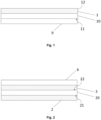
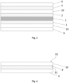
- Figures 1 to 5 show a schematic view of some steps of manufacturing of an optic arrangement according to the invention.
- a first transparent substrate 10 is provided.
- This first transparent substrate 10 comprises a first face 11 and a second face 12.
- a first transparent conductive electrode 1 is deposited on the second face 12 of the first transparent substrate 10, while an anti-coating element 9 is deposited on the first face 11 of the first transparent substrate 10.
- This deposition may be made by metal sputtering or metal coating.
- a second transparent substrate 20 is provided.
- This second transparent substrate 20 comprises a first face 21 and a second face 22.
- a second transparent conductive electrode 2 is deposited on the first face 21 of the second transparent substrate 20 and a third transparent conductive electrode 3 is deposited on the second face 22 of the second transparent substrate 20.
- an ion-storage layer 6 is deposited on the third transparent conductive electrode 3.
- a guest-host polymer dispersed liquid crystal film 5 is encapsulated and cured between the first transparent conductive electrode 1 (which is part of the assembly obtained in Figure 1 ) and the second transparent conductive electrode 2 (which is part of the assembly obtained in Figure 2 ).
- the Guest-Host Polymer Dispersed Liquid Crystal (GH-PDLC) is an element which comprises a dichroic dye in liquid crystal.
- the dichroic dyes act as functional dyes with ability to change its orientation. This change of orientation of the dye, in addition to the behaviour of the liquid crystal, produces a very high level of opacity in off-position and a very high level of transparency in On-position.
- a third transparent substrate 30 comprising a first face 31 and a second face 32 is provided. Then, a fourth transparent conductive electrode 4 is deposited on the first face 31 of the third transparent substrate 30. After this, an electrochromic layer 8 is deposited on the fourth transparent conductive electrode 4.
- Figure 5 shows an electrolyte layer 7 which is encapsulated and cured between the ion-storage layer 6 (which is part of the assembly obtained in Figure 3 ) and the electrochromic layer 8 (which is part of the assembly obtained in Figure 4 ).
- an electronic assembly is connected to the final structure, the electronic assembly being configured to provide a first electric signal to the first transparent conductive electrode 1, a second electric signal to the second transparent conductive electrode 2, a third electric signal to the third transparent conductive electrode 3 and a fourth electric signal to the fourth transparent conductive electrode 4.
- the first transparent conductive electrode 1 and the second transparent conductive electrode 2 usually employs Indium Tin Oxide, while the third transparent conductive electrode 3 and the fourth transparent conductive electrode 4 comprises silver nanowires.
- Electrochromic materials can be activated when desired to create an infrared barrier or a customized colour pattern. With this barrier, an amount of thermal energy may be saved at a cost of a little electrical energy supplied to the electrochromic layers. Also, the active optical material provides an ultraviolet barrier if desired, so that an advantageous combination of both works for an even better thermal barrier.
- This optical device can be used in different situations.
- a first situation can be the following one.
- the first signal and the second signal are the same (thus causing no voltage between the two sides of the PDLC material)
- the PDLC material remains opaque, thus providing an ultraviolet barrier and privacy protection from the outside.
- the third and fourth signals may be the same or different. If they are different, the electrochromic layer is activated and the corresponding colour (e.g., blue) can be seen. If they are the same, the electrochromic layer is not activated, so the colour will be the one of the PDLC material.
- the PDLC material becomes transparent.
- the third and fourth signals may be the same or different. If they are different, the electrochromic layer is activated and the corresponding colour (e.g., blue) can be seen in a transparent mode. If they are the same, the electrochromic layer is not activated, so the assembly will be totally transparent.
- the first transparent substrate, the second transparent substrate and the third transparent substrate comprises a glass.
- a glass is useful to install the optical arrangement in a building, where a physical separation is needed between two different spaces, and there are different needs of transparency and intimacy.
- a second situation can be exemplified as follows.
- the first transparent conductive electrode is divided into sections, each first section being electrically isolated with respect to the rest of the first sections.
- the electronic arrangement is now configured to feed each one of the sections with a different signal, to selectively activate or deactivate any of the sections, thus creating said patterns.
- These patterns can be combined with the operation of the electrochromic device, so that these sections can be fully transparent, with a coloured transparency, opaque with colour or opaque without colour.
- the first transparent substrate, the second transparent substrate and the third transparent substrate comprises polyethylene terephthalate.
- a flexible arrangement such as this polymeric example, may be attached to structures which are already built, thus conferring all the advantages of the invention without the need of re-installing the complete structure.
Landscapes
- Physics & Mathematics (AREA)
- Nonlinear Science (AREA)
- General Physics & Mathematics (AREA)
- Optics & Photonics (AREA)
- Chemical & Material Sciences (AREA)
- Crystallography & Structural Chemistry (AREA)
- Dispersion Chemistry (AREA)
- Mathematical Physics (AREA)
- Electrochromic Elements, Electrophoresis, Or Variable Reflection Or Absorption Elements (AREA)
Priority Applications (1)
| Application Number | Priority Date | Filing Date | Title |
|---|---|---|---|
| EP23382955.5A EP4528365A1 (fr) | 2023-09-21 | 2023-09-21 | Agencement de film intelligent pour de multiples utilisations et procédé de fabrication d'un agencement de film intelligent |
Applications Claiming Priority (1)
| Application Number | Priority Date | Filing Date | Title |
|---|---|---|---|
| EP23382955.5A EP4528365A1 (fr) | 2023-09-21 | 2023-09-21 | Agencement de film intelligent pour de multiples utilisations et procédé de fabrication d'un agencement de film intelligent |
Publications (1)
| Publication Number | Publication Date |
|---|---|
| EP4528365A1 true EP4528365A1 (fr) | 2025-03-26 |
Family
ID=88146840
Family Applications (1)
| Application Number | Title | Priority Date | Filing Date |
|---|---|---|---|
| EP23382955.5A Withdrawn EP4528365A1 (fr) | 2023-09-21 | 2023-09-21 | Agencement de film intelligent pour de multiples utilisations et procédé de fabrication d'un agencement de film intelligent |
Country Status (1)
| Country | Link |
|---|---|
| EP (1) | EP4528365A1 (fr) |
Citations (3)
| Publication number | Priority date | Publication date | Assignee | Title |
|---|---|---|---|---|
| US20100182673A1 (en) * | 2009-01-19 | 2010-07-22 | Samsung Electronics Co., Ltd. | Display devices using electrochromism and polymer dispersed liquid crystal and methods of driving the same |
| DE102011015950A1 (de) * | 2011-04-02 | 2012-10-04 | Daimler Ag | Optisches Bauteil und Verfahren zu dessen Herstellung |
| WO2023072673A1 (fr) * | 2021-10-28 | 2023-05-04 | Saint-Gobain Glass France | Procédé de commutation d'une vitre composite comprenant un élément fonctionnel électrochrome |
-
2023
- 2023-09-21 EP EP23382955.5A patent/EP4528365A1/fr not_active Withdrawn
Patent Citations (3)
| Publication number | Priority date | Publication date | Assignee | Title |
|---|---|---|---|---|
| US20100182673A1 (en) * | 2009-01-19 | 2010-07-22 | Samsung Electronics Co., Ltd. | Display devices using electrochromism and polymer dispersed liquid crystal and methods of driving the same |
| DE102011015950A1 (de) * | 2011-04-02 | 2012-10-04 | Daimler Ag | Optisches Bauteil und Verfahren zu dessen Herstellung |
| WO2023072673A1 (fr) * | 2021-10-28 | 2023-05-04 | Saint-Gobain Glass France | Procédé de commutation d'une vitre composite comprenant un élément fonctionnel électrochrome |
Similar Documents
| Publication | Publication Date | Title |
|---|---|---|
| US11724964B2 (en) | Multi-pane electrochromic windows | |
| US5604626A (en) | Photochromic devices | |
| US5197242A (en) | Dual-pane thermal window with liquid crystal shade | |
| EP2673674B1 (fr) | Dispositifs multicouches électrochromiques à commutation coordonnée spatialement | |
| Lampert | Smart switchable glazing for solar energy and daylight control | |
| US4848875A (en) | Dual-pane thermal window with liquid crystal shade | |
| US5009044A (en) | Dual-pane thermal window with liquid crystal shade | |
| Lampert | Optical switching technology for glazings | |
| US5111629A (en) | Dual-pane thermal window with liquid crystal shade | |
| US7999992B2 (en) | Charge conducting medium | |
| US4893902A (en) | Dual-pane thermal window with liquid crystal shade | |
| US4964251A (en) | Dual-pane thermal window with liquid crystal shade | |
| US4899503A (en) | Dual-pane thermal window with liquid crystal shade | |
| US5025602A (en) | Dual-pane thermal window with liquid crystal shade | |
| US20080030832A1 (en) | Multi-layer light modulator | |
| JP2025182115A (ja) | 多機能の調光フィルムおよびこのフィルムを含む構造体 | |
| KR20150086892A (ko) | 적외선 차단용 스마트 윈도우 | |
| CN101089716A (zh) | 压感电致变色组件及其制造方法 | |
| KR101448673B1 (ko) | 전기 변색 필름 및 이의 제조방법 | |
| EP4528365A1 (fr) | Agencement de film intelligent pour de multiples utilisations et procédé de fabrication d'un agencement de film intelligent | |
| WO2003098271A2 (fr) | Element electro-optique transmissif et ensemble a vitres dote dudit element | |
| KR102470079B1 (ko) | 변색 나노 입자, 이를 포함하는 변색 장치 및 이를 포함하는 표시 장치 | |
| Lampert | Smart windows switch on the light | |
| KR20250033458A (ko) | 복수개 반사 및 투과 패널의 구동 특성을 이용한 스위칭 윈도우 패널 | |
| Deb et al. | Atlas Standards Guide (Weather-Ometer, USA) 101 279 atomic layer deposition (ALD) 413 spatial ALD 413–415 automotive chromogenic products 8–9 |
Legal Events
| Date | Code | Title | Description |
|---|---|---|---|
| PUAI | Public reference made under article 153(3) epc to a published international application that has entered the european phase |
Free format text: ORIGINAL CODE: 0009012 |
|
| STAA | Information on the status of an ep patent application or granted ep patent |
Free format text: STATUS: THE APPLICATION HAS BEEN PUBLISHED |
|
| AK | Designated contracting states |
Kind code of ref document: A1 Designated state(s): AL AT BE BG CH CY CZ DE DK EE ES FI FR GB GR HR HU IE IS IT LI LT LU LV MC ME MK MT NL NO PL PT RO RS SE SI SK SM TR |
|
| STAA | Information on the status of an ep patent application or granted ep patent |
Free format text: STATUS: THE APPLICATION IS DEEMED TO BE WITHDRAWN |
|
| 18D | Application deemed to be withdrawn |
Effective date: 20250927 |