EP4528809A1 - Attache - Google Patents
Attache Download PDFInfo
- Publication number
- EP4528809A1 EP4528809A1 EP23199072.2A EP23199072A EP4528809A1 EP 4528809 A1 EP4528809 A1 EP 4528809A1 EP 23199072 A EP23199072 A EP 23199072A EP 4528809 A1 EP4528809 A1 EP 4528809A1
- Authority
- EP
- European Patent Office
- Prior art keywords
- clip
- metallic layer
- semi
- joint
- die
- Prior art date
- Legal status (The legal status is an assumption and is not a legal conclusion. Google has not performed a legal analysis and makes no representation as to the accuracy of the status listed.)
- Pending
Links
Images


Classifications
-
- H—ELECTRICITY
- H10—SEMICONDUCTOR DEVICES; ELECTRIC SOLID-STATE DEVICES NOT OTHERWISE PROVIDED FOR
- H10W—GENERIC PACKAGES, INTERCONNECTIONS, CONNECTORS OR OTHER CONSTRUCTIONAL DETAILS OF DEVICES COVERED BY CLASS H10
- H10W70/00—Package substrates; Interposers; Redistribution layers [RDL]
- H10W70/40—Leadframes
- H10W70/481—Leadframes for devices being provided for in groups H10D8/00 - H10D48/00
-
- H—ELECTRICITY
- H10—SEMICONDUCTOR DEVICES; ELECTRIC SOLID-STATE DEVICES NOT OTHERWISE PROVIDED FOR
- H10W—GENERIC PACKAGES, INTERCONNECTIONS, CONNECTORS OR OTHER CONSTRUCTIONAL DETAILS OF DEVICES COVERED BY CLASS H10
- H10W70/00—Package substrates; Interposers; Redistribution layers [RDL]
- H10W70/40—Leadframes
- H10W70/456—Materials
-
- H—ELECTRICITY
- H10—SEMICONDUCTOR DEVICES; ELECTRIC SOLID-STATE DEVICES NOT OTHERWISE PROVIDED FOR
- H10W—GENERIC PACKAGES, INTERCONNECTIONS, CONNECTORS OR OTHER CONSTRUCTIONAL DETAILS OF DEVICES COVERED BY CLASS H10
- H10W70/00—Package substrates; Interposers; Redistribution layers [RDL]
- H10W70/40—Leadframes
- H10W70/464—Additional interconnections in combination with leadframes
- H10W70/466—Tape carriers or flat leads
-
- H—ELECTRICITY
- H10—SEMICONDUCTOR DEVICES; ELECTRIC SOLID-STATE DEVICES NOT OTHERWISE PROVIDED FOR
- H10W—GENERIC PACKAGES, INTERCONNECTIONS, CONNECTORS OR OTHER CONSTRUCTIONAL DETAILS OF DEVICES COVERED BY CLASS H10
- H10W72/00—Interconnections or connectors in packages
- H10W72/071—Connecting or disconnecting
- H10W72/073—Connecting or disconnecting of die-attach connectors
-
- H—ELECTRICITY
- H10—SEMICONDUCTOR DEVICES; ELECTRIC SOLID-STATE DEVICES NOT OTHERWISE PROVIDED FOR
- H10W—GENERIC PACKAGES, INTERCONNECTIONS, CONNECTORS OR OTHER CONSTRUCTIONAL DETAILS OF DEVICES COVERED BY CLASS H10
- H10W72/00—Interconnections or connectors in packages
- H10W72/071—Connecting or disconnecting
- H10W72/076—Connecting or disconnecting of strap connectors
-
- H—ELECTRICITY
- H10—SEMICONDUCTOR DEVICES; ELECTRIC SOLID-STATE DEVICES NOT OTHERWISE PROVIDED FOR
- H10W—GENERIC PACKAGES, INTERCONNECTIONS, CONNECTORS OR OTHER CONSTRUCTIONAL DETAILS OF DEVICES COVERED BY CLASS H10
- H10W72/00—Interconnections or connectors in packages
- H10W72/30—Die-attach connectors
-
- H—ELECTRICITY
- H10—SEMICONDUCTOR DEVICES; ELECTRIC SOLID-STATE DEVICES NOT OTHERWISE PROVIDED FOR
- H10W—GENERIC PACKAGES, INTERCONNECTIONS, CONNECTORS OR OTHER CONSTRUCTIONAL DETAILS OF DEVICES COVERED BY CLASS H10
- H10W72/00—Interconnections or connectors in packages
- H10W72/60—Strap connectors, e.g. thick copper clips for grounding of power devices
-
- H—ELECTRICITY
- H10—SEMICONDUCTOR DEVICES; ELECTRIC SOLID-STATE DEVICES NOT OTHERWISE PROVIDED FOR
- H10W—GENERIC PACKAGES, INTERCONNECTIONS, CONNECTORS OR OTHER CONSTRUCTIONAL DETAILS OF DEVICES COVERED BY CLASS H10
- H10W72/00—Interconnections or connectors in packages
- H10W72/071—Connecting or disconnecting
- H10W72/073—Connecting or disconnecting of die-attach connectors
- H10W72/07331—Connecting techniques
- H10W72/07336—Soldering or alloying
-
- H—ELECTRICITY
- H10—SEMICONDUCTOR DEVICES; ELECTRIC SOLID-STATE DEVICES NOT OTHERWISE PROVIDED FOR
- H10W—GENERIC PACKAGES, INTERCONNECTIONS, CONNECTORS OR OTHER CONSTRUCTIONAL DETAILS OF DEVICES COVERED BY CLASS H10
- H10W72/00—Interconnections or connectors in packages
- H10W72/071—Connecting or disconnecting
- H10W72/073—Connecting or disconnecting of die-attach connectors
- H10W72/07341—Controlling the bonding environment, e.g. atmosphere composition or temperature
-
- H—ELECTRICITY
- H10—SEMICONDUCTOR DEVICES; ELECTRIC SOLID-STATE DEVICES NOT OTHERWISE PROVIDED FOR
- H10W—GENERIC PACKAGES, INTERCONNECTIONS, CONNECTORS OR OTHER CONSTRUCTIONAL DETAILS OF DEVICES COVERED BY CLASS H10
- H10W72/00—Interconnections or connectors in packages
- H10W72/071—Connecting or disconnecting
- H10W72/073—Connecting or disconnecting of die-attach connectors
- H10W72/07351—Connecting or disconnecting of die-attach connectors characterised by changes in properties of the die-attach connectors during connecting
- H10W72/07355—Connecting or disconnecting of die-attach connectors characterised by changes in properties of the die-attach connectors during connecting changes in materials
-
- H—ELECTRICITY
- H10—SEMICONDUCTOR DEVICES; ELECTRIC SOLID-STATE DEVICES NOT OTHERWISE PROVIDED FOR
- H10W—GENERIC PACKAGES, INTERCONNECTIONS, CONNECTORS OR OTHER CONSTRUCTIONAL DETAILS OF DEVICES COVERED BY CLASS H10
- H10W72/00—Interconnections or connectors in packages
- H10W72/071—Connecting or disconnecting
- H10W72/076—Connecting or disconnecting of strap connectors
- H10W72/07631—Techniques
- H10W72/07636—Soldering or alloying
-
- H—ELECTRICITY
- H10—SEMICONDUCTOR DEVICES; ELECTRIC SOLID-STATE DEVICES NOT OTHERWISE PROVIDED FOR
- H10W—GENERIC PACKAGES, INTERCONNECTIONS, CONNECTORS OR OTHER CONSTRUCTIONAL DETAILS OF DEVICES COVERED BY CLASS H10
- H10W72/00—Interconnections or connectors in packages
- H10W72/071—Connecting or disconnecting
- H10W72/076—Connecting or disconnecting of strap connectors
- H10W72/07641—Controlling the environment, e.g. atmosphere composition or temperature
-
- H—ELECTRICITY
- H10—SEMICONDUCTOR DEVICES; ELECTRIC SOLID-STATE DEVICES NOT OTHERWISE PROVIDED FOR
- H10W—GENERIC PACKAGES, INTERCONNECTIONS, CONNECTORS OR OTHER CONSTRUCTIONAL DETAILS OF DEVICES COVERED BY CLASS H10
- H10W72/00—Interconnections or connectors in packages
- H10W72/071—Connecting or disconnecting
- H10W72/076—Connecting or disconnecting of strap connectors
- H10W72/07651—Connecting or disconnecting of strap connectors characterised by changes in properties of the strap connectors during connecting
- H10W72/07655—Connecting or disconnecting of strap connectors characterised by changes in properties of the strap connectors during connecting changes in materials
-
- H—ELECTRICITY
- H10—SEMICONDUCTOR DEVICES; ELECTRIC SOLID-STATE DEVICES NOT OTHERWISE PROVIDED FOR
- H10W—GENERIC PACKAGES, INTERCONNECTIONS, CONNECTORS OR OTHER CONSTRUCTIONAL DETAILS OF DEVICES COVERED BY CLASS H10
- H10W72/00—Interconnections or connectors in packages
- H10W72/30—Die-attach connectors
- H10W72/331—Shapes of die-attach connectors
- H10W72/334—Cross-sectional shape, i.e. in side view
-
- H—ELECTRICITY
- H10—SEMICONDUCTOR DEVICES; ELECTRIC SOLID-STATE DEVICES NOT OTHERWISE PROVIDED FOR
- H10W—GENERIC PACKAGES, INTERCONNECTIONS, CONNECTORS OR OTHER CONSTRUCTIONAL DETAILS OF DEVICES COVERED BY CLASS H10
- H10W72/00—Interconnections or connectors in packages
- H10W72/30—Die-attach connectors
- H10W72/341—Dispositions of die-attach connectors, e.g. layouts
- H10W72/342—Dispositions of die-attach connectors, e.g. layouts relative to the surface, e.g. recessed, protruding
-
- H—ELECTRICITY
- H10—SEMICONDUCTOR DEVICES; ELECTRIC SOLID-STATE DEVICES NOT OTHERWISE PROVIDED FOR
- H10W—GENERIC PACKAGES, INTERCONNECTIONS, CONNECTORS OR OTHER CONSTRUCTIONAL DETAILS OF DEVICES COVERED BY CLASS H10
- H10W72/00—Interconnections or connectors in packages
- H10W72/30—Die-attach connectors
- H10W72/351—Materials of die-attach connectors
- H10W72/352—Materials of die-attach connectors comprising metals or metalloids, e.g. solders
- H10W72/3528—Intermetallic compounds
-
- H—ELECTRICITY
- H10—SEMICONDUCTOR DEVICES; ELECTRIC SOLID-STATE DEVICES NOT OTHERWISE PROVIDED FOR
- H10W—GENERIC PACKAGES, INTERCONNECTIONS, CONNECTORS OR OTHER CONSTRUCTIONAL DETAILS OF DEVICES COVERED BY CLASS H10
- H10W72/00—Interconnections or connectors in packages
- H10W72/60—Strap connectors, e.g. thick copper clips for grounding of power devices
- H10W72/621—Structures or relative sizes of strap connectors
- H10W72/625—Strap connectors having a filler embedded in a matrix
-
- H—ELECTRICITY
- H10—SEMICONDUCTOR DEVICES; ELECTRIC SOLID-STATE DEVICES NOT OTHERWISE PROVIDED FOR
- H10W—GENERIC PACKAGES, INTERCONNECTIONS, CONNECTORS OR OTHER CONSTRUCTIONAL DETAILS OF DEVICES COVERED BY CLASS H10
- H10W72/00—Interconnections or connectors in packages
- H10W72/60—Strap connectors, e.g. thick copper clips for grounding of power devices
- H10W72/631—Shapes of strap connectors
- H10W72/634—Cross-sectional shape
-
- H—ELECTRICITY
- H10—SEMICONDUCTOR DEVICES; ELECTRIC SOLID-STATE DEVICES NOT OTHERWISE PROVIDED FOR
- H10W—GENERIC PACKAGES, INTERCONNECTIONS, CONNECTORS OR OTHER CONSTRUCTIONAL DETAILS OF DEVICES COVERED BY CLASS H10
- H10W72/00—Interconnections or connectors in packages
- H10W72/60—Strap connectors, e.g. thick copper clips for grounding of power devices
- H10W72/641—Dispositions of strap connectors
- H10W72/646—Dispositions of strap connectors the connected ends being on auxiliary connecting means on bond pads, e.g. on a bump connector
-
- H—ELECTRICITY
- H10—SEMICONDUCTOR DEVICES; ELECTRIC SOLID-STATE DEVICES NOT OTHERWISE PROVIDED FOR
- H10W—GENERIC PACKAGES, INTERCONNECTIONS, CONNECTORS OR OTHER CONSTRUCTIONAL DETAILS OF DEVICES COVERED BY CLASS H10
- H10W72/00—Interconnections or connectors in packages
- H10W72/60—Strap connectors, e.g. thick copper clips for grounding of power devices
- H10W72/651—Materials of strap connectors
- H10W72/652—Materials of strap connectors comprising metals or metalloids, e.g. silver
- H10W72/6528—Intermetallic compounds
-
- H—ELECTRICITY
- H10—SEMICONDUCTOR DEVICES; ELECTRIC SOLID-STATE DEVICES NOT OTHERWISE PROVIDED FOR
- H10W—GENERIC PACKAGES, INTERCONNECTIONS, CONNECTORS OR OTHER CONSTRUCTIONAL DETAILS OF DEVICES COVERED BY CLASS H10
- H10W72/00—Interconnections or connectors in packages
- H10W72/60—Strap connectors, e.g. thick copper clips for grounding of power devices
- H10W72/651—Materials of strap connectors
- H10W72/655—Materials of strap connectors of outermost layers of multilayered strap connectors, e.g. material of a coating
-
- H—ELECTRICITY
- H10—SEMICONDUCTOR DEVICES; ELECTRIC SOLID-STATE DEVICES NOT OTHERWISE PROVIDED FOR
- H10W—GENERIC PACKAGES, INTERCONNECTIONS, CONNECTORS OR OTHER CONSTRUCTIONAL DETAILS OF DEVICES COVERED BY CLASS H10
- H10W72/00—Interconnections or connectors in packages
- H10W72/90—Bond pads, in general
- H10W72/951—Materials of bond pads
-
- H—ELECTRICITY
- H10—SEMICONDUCTOR DEVICES; ELECTRIC SOLID-STATE DEVICES NOT OTHERWISE PROVIDED FOR
- H10W—GENERIC PACKAGES, INTERCONNECTIONS, CONNECTORS OR OTHER CONSTRUCTIONAL DETAILS OF DEVICES COVERED BY CLASS H10
- H10W90/00—Package configurations
- H10W90/701—Package configurations characterised by the relative positions of pads or connectors relative to package parts
- H10W90/731—Package configurations characterised by the relative positions of pads or connectors relative to package parts of die-attach connectors
- H10W90/736—Package configurations characterised by the relative positions of pads or connectors relative to package parts of die-attach connectors between a chip and a stacked lead frame, conducting package substrate or heat sink
-
- H—ELECTRICITY
- H10—SEMICONDUCTOR DEVICES; ELECTRIC SOLID-STATE DEVICES NOT OTHERWISE PROVIDED FOR
- H10W—GENERIC PACKAGES, INTERCONNECTIONS, CONNECTORS OR OTHER CONSTRUCTIONAL DETAILS OF DEVICES COVERED BY CLASS H10
- H10W90/00—Package configurations
- H10W90/701—Package configurations characterised by the relative positions of pads or connectors relative to package parts
- H10W90/761—Package configurations characterised by the relative positions of pads or connectors relative to package parts of strap connectors
- H10W90/766—Package configurations characterised by the relative positions of pads or connectors relative to package parts of strap connectors between a chip and a stacked lead frame, conducting package substrate or heat sink
Definitions
- the present invention relates to a clip for a semi-conductor device, to a semi-conductor device that comprises the clip, and to a method of manufacturing the semi-conductor device.
- Semiconductor assemblies such as transistors, are manufactured as layered assemblies including components such as die paddles, dies, clips and a casing.
- the casing provides a protective functionality and at least partially surrounds the die and other components that form a part of the semiconductor assembly.
- Semiconductor assemblies are subject to temperature fluctuations in use. These temperature fluctuations result in the expansion and contraction of the components of the clip.
- the coefficient of thermal expansion of each component is different, and so the amount by which each component expands and contracts as a result of temperature changes is also different.
- semi-conductor devices are subject to temperature fluctuations, and may in some applications experience temperatures over a 200°C or greater range. Therefore, semi-conductors are typically designed to withstand temperatures as low as -65°C (or lower), and up to 150°C (or higher). These fluctuations lead to variations in the sizes of the components of the devices due to thermal expansion.
- the clip is generally made from a different material to the die to which it is secured, and to the solder used to secure the clip to the die.
- the clip may be made from copper whereas the die may be made from silicone and the solder from a lead alloy. Each of these materials has a different coefficient of thermal expansion, and so each of the components expands and contracts with temperature changes at a different rate.
- the pore size of the foam may be at least 10 ⁇ m.
- the pore size of the foam may be up to 100 ⁇ m.
- the pore size may be up to 50 ⁇ m.
- the pore size may be at least 10 ⁇ m and/or up to 30 ⁇ m.
- the pore size may be 20 ⁇ m.
- the conductivity of the clip is inversely proportional to the pore size.
- the flexibility of the clip is proportional to the pore size. Where the pore size of the foam is at least 10 ⁇ m and up to 100 ⁇ m, the balance of the conductivity of the clip and the flexibility of the clip is advantageously optimised. This allows the clip to operate efficiently, while reducing the likelihood of delamination.
- the part or parts of the clip that is formed from a metallic foam may have a porosity of at least 30% and/or up to 80%.
- the conductivity of the clip is inversely proportional to porosity.
- the flexibility of the clip is proportional to porosity. Where the porosity of the clip is at least 30% and/or up to 80%, the balance of the conductivity of the clip and the flexibility of the clip is advantageously optimised. This allows the clip to operate efficiently, while reducing the likelihood of delamination.
- the metallic foam may be formed of copper.
- the metallic foam may be an open cell foam.
- the foam may be a reticulated foam.
- reticulated may be understood to mean that the material of the clip forms a network of interconnected branches. That is to say, one can move from one point of the clip to any other point whilst maintaining contact with the material of the clip.
- the clip is able to better absorb internal stresses that the clip may be subject to in use.
- the entirety of the clip may be formed from a metallic foam.
- a semi-conductor device comprises a lead frame that comprises a die attach portion and a lead portion; a semi-conductor die mounted on the die attach portion; and a clip according to the first aspect of the invention. At least part of the clip is secured to the semi-conductor die. At least part of the clip is secured to the lead portion.
- a method of manufacturing a semi-conductor device comprises providing a lead frame.
- the lead frame comprises a die attach portion and a lead portion.
- the method further comprises: attaching a semi-conductor die to the die attach portion of the leadframe; providing a first metallic layer to the semi-conductor die and providing a second metallic layer to the lead portion; providing the clip of the first aspect of the invention such that a first portion of the clip contacts the first metallic layer and a second portion of the clip contacts the second metallic layer; and heating the clip, the first metallic layer, and the second metallic layer such that the first metallic layer and the second metallic layer melt.
- the method may further comprise providing a cover.
- the cover may be provided such that it encapsulates the lead frame, preferably excluding at least part of any leads of the lead frame, the semi-conductor die, and the clip.
- Melting of the first metallic layer and of the second metallic layer may cause the first metallic layer and the second metallic layer to migrate into the clip to form a first joint and a second joint respectively.
- the first metallic layer and the second metallic layer may migrate into the clip by capillary action.
- the first joint may comprise a portion that is disposed in the region of the first portion of the clip and a portion that is disposed in the region of the first metallic layer.
- the second joint may comprise a portion that is disposed in the region of the second portion of the clip and a portion that is disposed in the region of the second metallic layer.
- the first joint and the second joint may be formed upon cooling of the assembly.
- the melting temperature of the first joint and of the second joint may be at least 400°C.
- the melting temperature of the first and second joints is at least 400°C
- the likelihood of the first and second joint melting while the semi-conductor device is being secured to an external circuit is reduced. Melting of the first and/or second joint while the semi-conductor device is being secured to an external circuit is undesirable because it can lead to a reduction in the strength of the joint. Therefore, reducing the likelihood of melting of the first and second joints reduces the likelihood of short circuiting and current leakage in use. Therefore, where the melting temperature of the first and second joints is at least 400°C, the semi-conductor device resulting from the method is advantageously more reliable.
- the first metallic layer and the second metallic layer may be formed from tin and the clip is formed from copper.
- the first joint and the second joint may be formed from a copper-tin intermetallic compound.
- the first metallic layer and the second metallic layer may be formed from pure tin.
- the use of solder to secure the clip to the die and lead frame is not necessary. Furthermore, the likelihood of the first and/or second joint melting during assembly of the semi-conductor device into an external circuit is reduced as compared to if a conventional solder material were used to connect the clip to the lead frame and die. Melting of conventional solder material during assembly can increase the likelihood of short circuiting and/or current leakage in use Re-melting of conventional solder reduces the maximum peak forward surge current of semi-conductor devices. Therefore, by reducing the likelihood of the first and/or second joint melting during assembly of the semi-conductor device into an external circuit, the maximum peak forward surge current is improved.. Therefore, where the metallic layers are formed from tin and the clip is formed from copper, the semi-conductor device resulting from the method is advantageously more reliable.
- first metallic layer nor the second metallic layer may be formed from lead.
- Lead waste can contaminate the environment. Where neither the first metallic layer nor the second metallic layer are formed from lead, the method is more environmentally friendly.
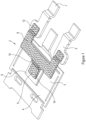
- Figure 1 shows a semiconductor device 2.
- the semi-conductor device 2 comprises a lead frame 4.
- the lead frame 4 may also be referred to as a die paddle.
- the semi-conductor device 2 comprises a die 6.
- the semi-conductor device 2 comprises a clip 8.
- the semi-conductor device 2 comprises a cover (not shown in Figure 1 for clarity).
- the lead frame 4 serves as a base of the semi-conductor device 2 to which other components of the device are attached.
- the lead frame 4 comprises a die attach portion 3.
- the die 6 is secured to the die attach portion 3.
- the lead frame 4 comprises a lead portion 5.
- the lead portion 5 comprises a plurality of leads 7 (only one of which is labelled in Figure 1 ).
- the plurality of leads allow the semiconductor device 2 to be connected to an external circuit (not shown).
- Each portion of the lead frame 4 is generally rectangular. However, in other embodiments, the portions of the lead frame may be any suitable shape.
- the lead frame 4 is manufactured from a conductive material such as copper (including a copper alloy).
- the lead portion 5 is separately formed from the die attach portion 3. However, in some embodiments, the lead portion 5 and the die attach portion may be integrally formed.
- the die 6 is secured to the lead frame 4.
- the die 6 is secured to the lead frame 4 by virtue of a first solder layer 10.
- the die 6 is secured to the die attach portion 3 of the lead frame 4 by the first solder layer 10.
- the die 6 may be a single component or may comprise multiple constituent components.
- the die 6 is made of a semi-conducting material.
- the die 6 has a functional circuit fabricated thereon.
- the die 6 is generally rectangular but may be any other suitable shape.
- the die 6 is plate like in shape.
- the cover encapsulates the components of the semi-conductor device 2 (i.e., the lead frame 4, the die 6, and the clip 8).
- the leads 7 of the clip 8 extend through the cover. This allows the leads 7 to be connected to the external circuit (not shown).
- the cover may be made from any suitable electrically isolating material, such as an epoxy.
- the cover may also be referred to as an isolator, a casing, or an encapsulant.
- the clip 8 comprises a first portion 9, a second portion 13, and an intermediate portion 15.
- the second portion 13 comprises a first arm 17 and a second arm 19. However, in some embodiments, the second portion 13 may comprise only a single arm.
- the intermediate portion 15 adjoins and is disposed between the first portion 9 and the second portion 13.
- the clip 8 is secured to the die 6. In particular, the first portion 9 of the clip 8 is secured to the die 6.
- the clip 8 is secured to the lead portion 5 of the lead frame 4.
- the second portion 13 of the clip 8 is secured to the lead portion 5 of the lead frame 4.
- the clip 8 thus electrically connects the die 6 and the lead portion 5 of the lead frame 4.
- the clip 8 may otherwise be referred to as a connector.
- the clip 8 is formed from a metallic foam.
- the clip 8 may be formed from a copper foam.
- the clip may be formed from a nickel or silver foam. Copper is, however, preferred due to its thermal and electrical conductivity, availability, and cost.
- the entirety of the clip 8 may be formed from a metallic foam.
- the foam may be either open cell or closed cell.
- the foam from which the clip 8 is formed may have a pore size of at least 10 ⁇ m and/or up to 100 ⁇ m. In some embodiments, the pore size may be up to 50 ⁇ m. In some embodiments, the pore size may be at least 10 ⁇ m and/or up to 30 ⁇ m. In some embodiments, the pore size may be 20 ⁇ m. The pore size may be chosen based on the desired flexibility of the clip 8.
- the porosity of the clip 8 may be at least 30% and/or up to 80%.
- the porosity of the clip 8 may be chosen based on the desired flexibility of the clip 8.
- the clip 8 being formed from a foam increases the flexibility of the clip 8 as compared to if the clip 8 were formed from a continuous or solid material. This advantageously allows the clip 8 to absorb internal stresses that arise as a result of temperature fluctuations of the semi-conductor device 2 in use.
- the clip 8 being formed from a foam also better secures the cover to the clip 8. This is because cover at least partially enters the pores of the clip 8, which increases the contact area between the clip 8 and cover as compared to if the clip 8 were formed from a solid material.
- the clip 8 being able to better absorb internal stresses and the cover being better secured to the clip 8 advantageously reduce the likelihood of delamination of the components of the semi-conductor device 2 in use.
- first portion 9 and the second portion 13 are formed from a metallic foam.
- first portion 9 and distal regions 25, 27 of the first and second arms 17, 19 of the second portion 13 may be formed from a metallic foam.
- a first metallic layer 20 is applied to the die 6.
- the first metallic layer 20 may be applied using electroplating or sputtering. These methods of application are advantageously more efficient that the conventional soldering method. This is because electroplating or sputtering of the first metallic layer 20 can take place during assembly of other components onto the die 6 using the same method.
- the first metallic layer 20 may be at least 2 ⁇ m and/or up to 10 ⁇ m thick.
- the thickness of the first metallic layer 20 may be chosen based on, for example, the desired contact area between the die 6 and the clip 8, the size of the clip 8 and of the semi-conductor device 2.
- a second metallic layer 22 is applied to the lead portion 5 of the lead frame 4.
- the second metallic layer 22 may be applied using electroplating.
- the second metallic layer 22 may be at least 2 ⁇ m and/or up to 10 ⁇ m thick.
- the thickness of the second metallic layer 22 may be chosen based on, for example, the size of the clip 2 and of the semi-conductor device 2.
- the first metallic layer 20 and the second metallic layer 22 may be formed from tin, preferably pure tin. In some embodiments, the first metallic layer 20 and/or the second metallic layer 22 may be formed from indium.
- the material of the first metallic layer 20 and the second metallic layer 22 may be chosen based on the material from which the clip 8 is made. In some embodiments, neither the first metallic layer 20 nor the second metallic layer 22 contain lead.
- the clip 8 is then positioned such that the first portion 9 of the clip 8 contacts the first metallic layer 20 and the second portion 13 of the clip 8 contacts the second metallic layer 22.
- the resulting assembly 24 is shown in Figure 4 .
- the assembly 24 is then heated.
- the temperature to which the assembly 24 is heated is determined by the material from which the first metallic layer 20 and the second metallic layer 22 are made. In particular, the assembly 24 is heated to at least the melting temperature of the first metallic layer 20 and of the second metallic layer 22. Where the first metallic layer 20 and the second metallic layer 22 are formed from tin, preferably pure tin, the temperature to which the assembly 24 is heated may be at least 232°C.
- Melting of the first metallic layer 20 and of the second metallic layer 22 causes the first metallic layer 20 and the second metallic layer 22 to migrate into the clip 8.
- the first metallic layer 20 and of the second metallic layer 22 migrate into the clip 8 by capillary action.
- the first metallic layer 20 and the second metallic layer 22 migrate into the clip 8 in the region of the first portion 9 and the second portion 13 of the clip 8 respectively.
- some of the first metallic layer 20 and some of the second metallic layer 22 may migrate beyond the first portion 9 and beyond the second portion 13.
- Figure 5 shows the assembly 24 following cooling. Melting and cooling of the first metallic layer 20 results in the formation of a first joint 23.
- a portion of the first joint 23 is disposed in the region of the first portion 9 of the clip 8, and a portion is disposed in the region of the first metallic layer 20.
- the first joint 23 secures the first portion 9 of the clip 8 to the die 6.
- the first joint 23 is formed of an intermetallic compound.
- the intermetallic compound of the first joint 23 comprises the material from which the clip 8 is made (prior to heating) and the material from which the first metallic layer 20 is made (prior to heating).
- the intermetallic compound of the first joint 23 is a copper-tin compound.
- the intermetallic compound of the first joint 23 may be a nickel-tin compound, a silver-tin compound, or a copper-indium compound.
- the second joint 26 is formed of an intermetallic compound.
- the intermetallic compound of the second joint 26 comprises the material from which the clip 8 is made (prior to heating) and the material from which the second metallic layer 22 is made (prior to heating).
- the intermetallic compound of the second joint 26 is a copper-tin compound.
- the intermetallic compound of the second joint 26 may be a nickel-tin compound, a silver-tin compound, or a copper-indium compound.
- the intermetallic compound of the second joint 26 may be the same as the intermetallic compound of the first joint 23. Neither the intermetallic compound of the first joint 23 nor the intermetallic compound of the second joint 26 may be formed from or contain lead. This advantageously meets regulations which require lead-free semi-conductor devices.
- the cover 18 is then provided in a conventional manner.
Landscapes
- Lead Frames For Integrated Circuits (AREA)
- Die Bonding (AREA)
Priority Applications (3)
| Application Number | Priority Date | Filing Date | Title |
|---|---|---|---|
| EP23199072.2A EP4528809A1 (fr) | 2023-09-22 | 2023-09-22 | Attache |
| CN202411307274.5A CN119695019A (zh) | 2023-09-22 | 2024-09-19 | 夹片 |
| US18/889,545 US20250105198A1 (en) | 2023-09-22 | 2024-09-19 | Clip |
Applications Claiming Priority (1)
| Application Number | Priority Date | Filing Date | Title |
|---|---|---|---|
| EP23199072.2A EP4528809A1 (fr) | 2023-09-22 | 2023-09-22 | Attache |
Publications (1)
| Publication Number | Publication Date |
|---|---|
| EP4528809A1 true EP4528809A1 (fr) | 2025-03-26 |
Family
ID=88147140
Family Applications (1)
| Application Number | Title | Priority Date | Filing Date |
|---|---|---|---|
| EP23199072.2A Pending EP4528809A1 (fr) | 2023-09-22 | 2023-09-22 | Attache |
Country Status (3)
| Country | Link |
|---|---|
| US (1) | US20250105198A1 (fr) |
| EP (1) | EP4528809A1 (fr) |
| CN (1) | CN119695019A (fr) |
Families Citing this family (1)
| Publication number | Priority date | Publication date | Assignee | Title |
|---|---|---|---|---|
| USD1103797S1 (en) * | 2021-11-18 | 2025-12-02 | Agilent Technologies, Inc. | Capillary tag |
Citations (2)
| Publication number | Priority date | Publication date | Assignee | Title |
|---|---|---|---|---|
| US20180158757A1 (en) * | 2015-06-01 | 2018-06-07 | Siemens Aktiengesellschaft | Method for electrically contacting a component by galvanic connection of an open-pored contact piece, and corresponding component module |
| US20200105707A1 (en) * | 2018-10-02 | 2020-04-02 | Infineon Technologies Austria Ag | Multi-Clip Structure for Die Bonding |
-
2023
- 2023-09-22 EP EP23199072.2A patent/EP4528809A1/fr active Pending
-
2024
- 2024-09-19 US US18/889,545 patent/US20250105198A1/en active Pending
- 2024-09-19 CN CN202411307274.5A patent/CN119695019A/zh active Pending
Patent Citations (2)
| Publication number | Priority date | Publication date | Assignee | Title |
|---|---|---|---|---|
| US20180158757A1 (en) * | 2015-06-01 | 2018-06-07 | Siemens Aktiengesellschaft | Method for electrically contacting a component by galvanic connection of an open-pored contact piece, and corresponding component module |
| US20200105707A1 (en) * | 2018-10-02 | 2020-04-02 | Infineon Technologies Austria Ag | Multi-Clip Structure for Die Bonding |
Also Published As
| Publication number | Publication date |
|---|---|
| CN119695019A (zh) | 2025-03-25 |
| US20250105198A1 (en) | 2025-03-27 |
Similar Documents
| Publication | Publication Date | Title |
|---|---|---|
| US10727163B2 (en) | Semiconductor device | |
| KR100684240B1 (ko) | 반도체 장치 및 그 제조 방법 | |
| CN202454546U (zh) | 半导体器件 | |
| US8299600B2 (en) | Semiconductor device and manufacturing method thereof | |
| US20160126197A1 (en) | Semiconductor device having a stress-compensated chip electrode | |
| US20070125449A1 (en) | High-temperature solder, high-temperature solder paste and power semiconductor device using same | |
| US10830544B2 (en) | Self-healing metal structures | |
| US12394769B2 (en) | Batch soldering of different elements in power module | |
| US20250105198A1 (en) | Clip | |
| US9224698B1 (en) | Semiconductor device | |
| JPH0936186A (ja) | パワー半導体モジュール及びその実装方法 | |
| US12009332B2 (en) | Semiconductor device having high yield strength intermediate plate | |
| JPS6141135B2 (fr) | ||
| US20190189584A1 (en) | Semiconductor device and method for manufacturing the same | |
| JP2000323647A (ja) | モジュール型半導体装置及びその製造方法 | |
| JP3972519B2 (ja) | パワー半導体モジュール | |
| EP3890008A1 (fr) | Agencement de module semi-conducteur comprenant une couche de connexion avec une grille élastique entre une puce semi-conductrice et un substrat et procédé de fabrication d'un tel agencement | |
| JP7320446B2 (ja) | 半導体装置およびその製造方法 | |
| US20260005181A1 (en) | Semiconductor device and a method of manufacturing of the semiconductor device | |
| EP4661074A2 (fr) | Appareil à semi-conducteur, procédés de fabrication et systèmes électriques | |
| US20260096462A1 (en) | Clip-bonded semiconductor package and corresponding method of manufacturing such a semiconductor package | |
| EP0384645A1 (fr) | Matériau de brasure pour la formation d'une liaison entre une plaquette semi-conductrice et un contact métallique | |
| US20240297111A1 (en) | Carrier structure, package arrangement, method of forming a carrier structure, and method of forming a package arrangement | |
| US20250372569A1 (en) | Semiconductor apparatus, manufacturing methods, and electrical systems | |
| JPH11347785A (ja) | 半導体ダイボンディング用半田とそのテープ及び半導体装置 |
Legal Events
| Date | Code | Title | Description |
|---|---|---|---|
| PUAI | Public reference made under article 153(3) epc to a published international application that has entered the european phase |
Free format text: ORIGINAL CODE: 0009012 |
|
| STAA | Information on the status of an ep patent application or granted ep patent |
Free format text: STATUS: THE APPLICATION HAS BEEN PUBLISHED |
|
| AK | Designated contracting states |
Kind code of ref document: A1 Designated state(s): AL AT BE BG CH CY CZ DE DK EE ES FI FR GB GR HR HU IE IS IT LI LT LU LV MC ME MK MT NL NO PL PT RO RS SE SI SK SM TR |
|
| STAA | Information on the status of an ep patent application or granted ep patent |
Free format text: STATUS: REQUEST FOR EXAMINATION WAS MADE |
|
| 17P | Request for examination filed |
Effective date: 20250911 |
|
| REG | Reference to a national code |
Ref country code: DE Ref legal event code: R079 Free format text: PREVIOUS MAIN CLASS: H01L0023495000 Ipc: H10W0070400000 |
|
| RIC1 | Information provided on ipc code assigned before grant |
Ipc: H10W 70/40 20260101AFI20260129BHEP Ipc: H10W 72/00 20260101ALI20260129BHEP Ipc: H10W 72/60 20260101ALI20260129BHEP |
|
| GRAP | Despatch of communication of intention to grant a patent |
Free format text: ORIGINAL CODE: EPIDOSNIGR1 |
|
| STAA | Information on the status of an ep patent application or granted ep patent |
Free format text: STATUS: GRANT OF PATENT IS INTENDED |
|
| INTG | Intention to grant announced |
Effective date: 20260312 |