EP4529023A2 - Frequenzerzeugung eines mehrantennen-sende-empfangssystems - Google Patents
Frequenzerzeugung eines mehrantennen-sende-empfangssystems Download PDFInfo
- Publication number
- EP4529023A2 EP4529023A2 EP25156783.0A EP25156783A EP4529023A2 EP 4529023 A2 EP4529023 A2 EP 4529023A2 EP 25156783 A EP25156783 A EP 25156783A EP 4529023 A2 EP4529023 A2 EP 4529023A2
- Authority
- EP
- European Patent Office
- Prior art keywords
- transceiver
- chip
- frequency
- reference frequency
- antenna
- Prior art date
- Legal status (The legal status is an assumption and is not a legal conclusion. Google has not performed a legal analysis and makes no representation as to the accuracy of the status listed.)
- Pending
Links
Images


Classifications
-
- H—ELECTRICITY
- H04—ELECTRIC COMMUNICATION TECHNIQUE
- H04B—TRANSMISSION
- H04B1/00—Details of transmission systems, not covered by a single one of groups H04B3/00 - H04B13/00; Details of transmission systems not characterised by the medium used for transmission
- H04B1/38—Transceivers, i.e. devices in which transmitter and receiver form a structural unit and in which at least one part is used for functions of transmitting and receiving
- H04B1/40—Circuits
- H04B1/403—Circuits using the same oscillator for generating both the transmitter frequency and the receiver local oscillator frequency
-
- H—ELECTRICITY
- H04—ELECTRIC COMMUNICATION TECHNIQUE
- H04B—TRANSMISSION
- H04B1/00—Details of transmission systems, not covered by a single one of groups H04B3/00 - H04B13/00; Details of transmission systems not characterised by the medium used for transmission
- H04B1/02—Transmitters
- H04B1/04—Circuits
- H04B1/0475—Circuits with means for limiting noise, interference or distortion
Definitions
- the present disclosure relates generally to the field of multi-antenna transceiver systems. More particularly, it relates to generation of conversion frequencies in multi-antenna transceiver systems.
- a multi-antenna transceiver may be constructed using a plurality of transceiver chips, wherein each transceiver chip is associated with one or more corresponding antenna elements.
- a frequency generator can provide a signal indicative of a conversion frequency to each of the transceiver chips, for on-chip frequency conversion of a transceiver signal in each of the transceiver chips.
- the provision of the signal from the frequency generator to each of the transceiver chips may be problematic. Such problems may be particularly prominent for relatively high conversion frequencies. For example, transferring the signal between the frequency generator and a transceiver chip may introduce interference. Alternatively or additionally, transferring the signal between the frequency generator and a transceiver chip may cause power dissipation.
- the physical product may comprise one or more parts, such as controlling circuitry in the form of one or more controllers, one or more processors, or the like.
- a first aspect is a multi-antenna transceiver system comprising a group of transceiver chips and a reference frequency generator configured to provide a reference frequency for each transceiver chip of the group.
- Each transceiver chip has a respective chip-associated frequency generator configured to provide a respective conversion frequency based on the reference frequency, wherein each respective conversion frequency is higher than the reference frequency, and each transceiver chip is configured to use the respective conversion frequency for on-chip frequency conversion of a transceiver signal.
- the group of transceiver chips comprises two or more disjunct groups of transceiver chips and the reference frequency generator comprises a respective reference frequency generator for each group of transceiver chips.
- the reference frequency is provided directly to each transceiver chip of the group.
- the reference frequency is provided directly to a first transceiver chip of the group, and the reference frequency is provided via the first transceiver chip to a second transceiver chip of the group.
- the multi-antenna transceiver system further comprises baseband processing circuitry configured to process transceiver signals for the transceiver chips.
- the baseband processing circuitry is further configured to estimate a first respective phase shift of each respective chip-associated frequency generator, and compensate the transceiver signals based on the first respective phase shifts.
- the baseband processing circuitry is further configured to estimate a frequency error for the respective chip-associated frequency generators, and control the reference frequency generator based on the frequency error.
- the baseband processing circuitry is further configured to estimate baseband correlation timing for at least one transceiver chip, and control baseband correlation for at least one other transceiver chip based on the estimated baseband correlation timing.
- the baseband processing circuitry is further configured to acquire a second respective phase shift for each transceiver chip, and compensate the transceiver signals based on the second respective phase shifts.
- each respective conversion frequency is higher than 24 GHz (e.g., 24-300 GHz) and/or the reference frequency is lower than 1 GHz (e.g., 150-500 MHz).
- a second aspect is a baseband processor for a multi-antenna transceiver system.
- the baseband processor is configured to process transceiver signals for a group of transceiver chips comprised in the multi-antenna transceiver system, wherein each transceiver chip has a respective chip-associated frequency generator configured to provide a respective conversion frequency based on a reference frequency provided by a reference frequency generator comprised in the multi-antenna transceiver system, and wherein each respective conversion frequency is higher than the reference frequency.
- the baseband processor comprises baseband processing circuitry configured to estimate a first respective phase shift of each respective chip-associated frequency generator, and compensate the transceiver signals based on the first respective phase shifts.
- a third aspect is a network node comprising the multi-antenna transceiver system of the first aspect and/or the baseband processor of the second aspect.
- a fourth aspect is a wireless communication device comprising the multi-antenna transceiver system of the first aspect and/or the baseband processor of the second aspect.
- a fifth aspect is a method for operating a multi-antenna transceiver system comprising a group of transceiver chips and a reference frequency generator, wherein the reference frequency generator is configured to provide a reference frequency for each transceiver chip of the group, wherein each transceiver chip has a respective chip-associated frequency generator configured to provide a respective conversion frequency based on the reference frequency, each respective conversion frequency being higher than the reference frequency, and wherein each transceiver chip is configured to use the respective conversion frequency for on-chip frequency conversion of a transceiver signal.
- the method comprises estimating a first respective phase shift of each respective chip-associated frequency generator, and compensating the transceiver signal based on the first respective phase shifts.
- a sixth aspect is a computer program product comprising a non-transitory computer readable medium, having thereon a computer program comprising program instructions.
- the computer program is loadable into a data processing unit and configured to cause execution of the method according to the fifth aspect when the computer program is run by the data processing unit.
- any of the above aspects may additionally have features identical with or corresponding to any of the various features as explained above for any of the other aspects.
- An advantage of some embodiments is that alternative (e.g., improved) approaches to conversion frequency provision for multi-antenna transceiver systems are provided.
- An advantage of some embodiments is that interference and/or power dissipation caused by signal transfer between the common frequency generator and the transceiver chip is reduced compared to prior art approaches. Since the signal transfer is for the reference frequency - which is lower than the conversion frequency - transfer problems that are more severe at relatively high frequencies are mitigated. Signal transfer for the conversion frequency can be constrained to on-chip transfer only, or to between-chip distances which are comparatively short and/or otherwise advantageous.
- An advantage of some embodiments is that implementation, e.g., printed circuit board (PCB) design, for multi-antenna transceivers is simplified compared to the prior art. For example, the impact of any implementation process variations may be reduced.
- PCB printed circuit board
- An advantage of some embodiments is that received signal combining can be made coherently over transceiver chips. Since phase differences between transceiver chips (which is, e.g., introduced by phase offsets in the chip-associated frequency generators and/or due to phase shifts introduced by received signal transfer from the transceiver chips to the baseband circuitry) are estimated and compensated for, coherent combining is feasible.
- a functional unit of a transceiver chain e.g., ADC, DAC, frequency converter, mixer, filter, etc.
- ADC analog to digital converter
- DAC digital to analog converter
- mixer analog to digital converter
- filter filter
- Multi-antenna transceivers may be used for multiple-input multiple-output (MIMO; e.g., massive MIMO or traditional MIMO) communication and/or for beamformed communication (e.g., transmission pre-coding and/or reception combining).
- MIMO multiple-input multiple-output
- the baseband content is typically the same for some (e.g., all) transceiver chips, while the transmitted/received signals typically differ between antenna elements.
- the baseband processing may typically comprise processing of a radio signal which is simultaneously received or transmitted by the different antenna elements, on the same carrier frequency.
- the multi-antenna transceiver systems presented herein, or part thereof, may be particularly suitable for massive MIMO and/or beamforming.
- transceiver architectures for massive MIMO and/or beamforming may be implemented using analog multi-antenna control, digital multi-antenna control, or hybrid multi-antenna control.
- beamforming is typically performed at radio frequency (RF) using a bank of phase shifters (one per antenna element), an analog power combiner for the receiver, and a power splitter for the transmitter.
- RF radio frequency
- ADC analog-to-digital converter
- DAC digital-to-analog converter
- the antenna elements may be clustered and implemented in the form of an antenna panel.
- each transceiver chain requires an ADC instance (typically a pair of ADCs) and a DAC instance (typically a pair of DACs).
- a digital beamforming transceiver may be configured to simultaneously direct beams in, at least theoretically, an infinite number of directions.
- digital beamforming transceivers are superior at tracking radio signals (e.g., when mobile devices move fast relative to the radio base station).
- a (digital) multi-antenna transceiver may be constructed using a plurality of transceiver chips and a frequency generator providing a conversion frequency to each of the transceiver chips.
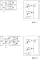
- FIG. 1 schematically illustrates an example multi-antenna transceiver system 100 with a plurality of transceiver chips (TX/RX) 101, 102 and a single frequency generator (FG) 110 providing the conversion frequency 111 to each of the transceiver chips.
- the example system 100 also comprises a baseband processor (BBP) 120 configured to process transceiver signals for the transceiver chips.
- BBP baseband processor
- FIG. 1 An example schematic architecture for a transceiver chip 101, 102 is illustrated in Figure 1 .
- the example architecture comprises a receiver path (RX) 191 and a transmitter path (TX) 192.
- the receiver path comprises a down-converter (DC) 195 and the transmitter path comprises an up-converter (UC) 196.
- the down-converter and up-converter each receives the conversion frequency from the frequency generator for on-chip frequency conversion of a transceiver signal (i.e., down-conversion of a received signal in the receiver path and/or up-conversion in the transmitter path of a signal to be transmitted).
- the receiver path 191 and the transmitter path 192 may generally comprise any suitable functional and/or physical components (e.g., as known in the art).
- the receiver path may, for example, comprise a low-noise amplifier (LNA), mixer circuitry (for down-conversion), one or more filters (e.g., a low-pass filter; LPF), and a variable gain amplifier.
- the transmitter may, for example, comprise one or more filters (e.g., a low-pass filter; LPF), mixer circuitry (for up-conversion), and a power amplifier (PA).
- LNA low-noise amplifier
- PA power amplifier
- the example architecture for a transceiver chip comprises a front end (FE) 194 and an interface (IF) 193.
- the interface 193 is for connection to the baseband processor 120, and can have any suitable functional and/or physical components (e.g., as known in the art).
- the front-end 194 may be for connection to one or more antenna elements or may comprise one or more on-chip antenna elements.
- each transceiver chip 101, 102 of the multi-antenna transceiver system 100 is associated with one or more corresponding antenna elements.
- the front-end 194 may comprise any suitable functional and/or physical components (e.g., as known in the art).
- the front end 194 may comprise duplexer or diplexer circuitry (e.g., switching circuitry, filters, etc.) for separation of received signals from signals to be transmitted.
- LO Local Oscillator
- f c frequency generator
- the phase shift is typically the same for all RF chips, so a channel estimator operating in baseband frequency may consider the unknown phase shift as part of the overall channel to be estimated.
- coherent combining of received signals S i ( t ) can be achieved without particularly addressing the unknown phase shift.
- the provision of the signal from the frequency generator to each of the transceiver chips may be problematic (e.g., in terms of interference and/or power dissipation); in particular for relatively high conversion frequencies.
- mmWave millimeter wavelength
- PCB Printed Circuit Board
- some embodiments are particularly suitable for scenarios with relatively high conversion frequency (e.g., mmW frequency), but application of the embodiments is not limited thereto.
- relatively high conversion frequency e.g., mmW frequency
- some embodiments are particularly suitable for massive MIMO and or precision beamforming, but application of the embodiments is not limited thereto.
- any of the multi-antenna transceiver systems, and/or transceiver chips/packages, and/or baseband processors, and/or frequency generators (reference, on-chip, or chip associated) described herein may be for (e.g., comprisable - or comprised - in) any suitable communication apparatus.
- Example suitable communication apparatuses include network nodes (e.g., base station, access point (AP), fixed wireless access (FWA) unit, non-terrestrial transceiver - such as satellite or unmanned aerial vehicle (UAV), etc.) and wireless communication devices (e.g., user equipment (UE), station (STA), Internet of Things (IoT) device, etc.).
- network nodes e.g., base station, access point (AP), fixed wireless access (FWA) unit, non-terrestrial transceiver - such as satellite or unmanned aerial vehicle (UAV), etc.
- wireless communication devices e.g., user equipment (UE), station (STA), Internet of Things (I
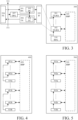
- FIG. 2 schematically illustrates an example multi-antenna transceiver system 200 according to some embodiments.
- the example system 200 has a plurality (e.g., a group) of transceiver chips (TX/RX) 201, 202 and a reference frequency generator (RFG) 210.
- the example system 200 may also comprise a baseband processor (BBP) 220 configured to process transceiver signals for the transceiver chips.
- the baseband circuitry may comprise one or more baseband processing chips.
- the reference frequency generator 210 is configured to provide a signal indicative of a frequency to each of the transceiver chips.
- the frequency provided by the reference frequency generator 210 in the example system 200 is a reference frequency 211, which is lower than the conversion frequency to be used for on-chip conversion in each of the transceiver chips (compare with 111 of Figure 1 ).
- the reference frequency generator 210 may be implemented in any suitable way.
- the reference frequency generator 210 may be a crystal oscillator (XO) and/or a voltage-controlled oscillator. Providing a relatively low frequency between chips typically causes less power dissipation and/or interference than providing a relatively high frequency between chips.
- an example architecture for the transceiver chips 201, 202 comprises a front end (FE) 294, an interface (IF) 293, a receiver path (RX) 291 and a transmitter path (TX) 292, wherein the receiver path comprises a down-converter (DC) 295 and the transmitter path comprises an up-converter (UC) 296.
- FE front end
- IF interface
- RX receiver path
- TX transmitter path
- DC down-converter
- UC up-converter
- the receiver path 291 and the transmitter path 292 may generally comprise any suitable functional and/or physical components.
- the receiver path may, for example, comprise a low-noise amplifier (LNA), mixer circuitry (for down-conversion), one or more filters (e.g., a low-pass filter; LPF), a variable gain amplifier, and possibly an analog-to-digital converter (ADC) instance.
- the transmitter may, for example, comprise one or more filters (e.g., a low-pass filter; LPF), mixer circuitry (for up-conversion), a power amplifier (PA) and possibly a digital-to-analog converter (DAC) instance.
- LNA low-noise amplifier
- LPF low-pass filter
- ADC analog-to-digital converter
- the transmitter may, for example, comprise one or more filters (e.g., a low-pass filter; LPF), mixer circuitry (for up-conversion), a power amplifier (PA) and possibly a digital-to-analog converter (DAC) instance
- the interface 293 is for connection to the baseband processor 220, and can have any suitable functional and/or physical components.
- the front-end 294 may be for connection to one or more antenna elements or may comprise one or more on-chip antenna elements.
- each transceiver chip 201, 202 of the multi-antenna transceiver system 200 is associated with one or more corresponding antenna elements.
- the front-end 294 may comprise any suitable functional and/or physical components.
- the front end 294 may comprise duplexer or diplexer circuitry (e.g., switching circuitry, filters, etc.) for separation of received signals from signals to be transmitted.
- a duplexer or diplexer may be implemented with Surface-Acoustic Wave (SAW) technology, Bulk-Acoustic Wave (BAW) technology, with waveguide technology, with lumped RLC elements (on-chip and/or discrete components), and/or with transmission-lines.
- SAW Surface-Acoustic Wave
- BAW Bulk-Acoustic Wave
- waveguide technology with lumped RLC elements (on-chip and/or discrete components), and/or with transmission-lines.
- the down-converter 295 and up-converter 296 of the example transceiver chip architecture of Figure 2 each receives a conversion frequency (for on-chip frequency conversion of a transceiver signal) from an on-chip frequency generator (OFG) 297.
- the on-chip frequency generator 297 is configured to provide the conversion frequency based on the reference frequency 211 provided by the reference frequency generator 210.
- the conversion frequency is higher than the reference frequency, but on-chip provision of a relatively high frequency is much less problematic (e.g., regarding power dissipation and/or interference) than provision between chips.
- the conversion frequency should be the same frequency for all of the transceiver chips. However, due to instantiation variations, the phase of the signal indicating the respective conversion frequency for each transceiver chip may differ. Alternatively or additionally, there may be minor frequency differences between the respective conversion frequency provided for each transceiver chip due to instantiation variations.
- the conversion frequency is higher than the reference frequency.
- the conversion frequency may be substantially higher than the reference frequency.
- the conversion frequency may be higher than 24 GHz and/or the reference frequency may be lower than 1 GHz.
- the frequency generator configured to provide the conversion frequency is an on-chip frequency generator (i.e., implemented on the transceiver chip; which may be an integrated circuit - IC - chip, for example) and the reference frequency is provided to each transceiver chip.
- the frequency generator configured to provide the conversion frequency may be implemented separately from (e.g., on a separate chip), but associated with, the transceiver chip; and the reference frequency may be provided to the frequency generator (i.e., for the transceiver chip).
- a chip-associated frequency generator may be implemented on a separate chip included in the same package (e.g., an encapsulation) as the transceiver chip.
- a chip-associated frequency generator is implemented on a separate chip included in the same package as the transceiver chip is termed system in package (SIP).
- SIP system in package
- a chip-associated frequency generator may be implemented on a separate chip with shorter and/or more efficient wiring to the transceiver chip (e.g., in package wiring) than the reference frequency generator would have.
- a chip-associated frequency generator may be shared by two or more - but not all - transceiver chips.
- the separate chip may implement other (e.g., digital) functionality in addition to the chip-associated frequency generation.
- the chip-associated frequency generator may be implemented using any suitable approach capable of generating an output frequency based on an input frequency.
- the chip-associated frequency generator may be implemented using a phase-locked loop (PLL).
- PLL phase-locked loop
- the reference frequency is provided directly to each transceiver chip 201, 202 (corresponding to the reference frequency being provided directly to each chip-associated frequency generator in the general case).
- the reference frequency 211 is provided in a parallel manner to the transceiver chips.
- FIG. 3 An alternative is illustrated in Figure 3 , where the reference frequency is provided directly to one, first, transceiver chip (or - generally - to one, first, chip-associated frequency generator) and to other transceiver chips (or - generally - to other chip-associated frequency generators) via the first transceiver chip (or - generally - via the first chip-associated frequency generator.
- FIG. 3 schematically illustrates an example multi-antenna transceiver system 300 according to some embodiments.
- the example system 300 has a plurality (e.g., a group) of transceiver chips (TX/RX) 301, 302 and a reference frequency generator (RFG) 310.
- the example system 300 may also comprise a baseband processor (BBP) 320 configured to process transceiver signals for the transceiver chips. Any aspects of the baseband processor 220 described in connection to Figure 2 may be applicable also for the baseband processor 320.
- BBP baseband processor
- the reference frequency generator 310 is configured to provide a signal indicative of a reference frequency 311 to each of the transceiver chips. Any aspects of the reference frequency generator 210 described in connection to Figure 2 may be applicable also for the reference frequency generator 310.
- the reference frequency 311 is not provided directly to each transceiver chip 301, 302. Instead, the reference frequency 311 is provided directly only to a first transceiver chip 302, and via the first transceiver chip 302 to the other transceiver chips 301.
- the reference frequency 311 is successively provided; from the first transceiver chip to a second transceiver chip, from the second transceiver chip to a third transceiver chip, and so on until the last transceiver chip (i.e., the reference frequency 311 is provided in a serial manner to the transceiver chips).
- the reference frequency being provided from the first transceiver chip to more than one second transceiver chip.
- an example architecture for the transceiver chips 301, 302 comprises a front end (FE) 394, an interface (IF) 393, a receiver path (RX) 391 and a transmitter path (TX) 392, wherein the receiver path comprises a down-converter (DC) 395 and the transmitter path comprises an up-converter (UC) 396, each receiving a conversion frequency (for on-chip frequency conversion of a transceiver signal) from an on-chip, or - generally - chip-associated, frequency generator (OFG) 397.
- Any aspects of the example schematic architecture described in connection to Figure 2 may be applicable also for the example schematic architecture of Figure 3 .
- At least one (e.g., the first) transceiver chip (typically all transceiver chips) of Figure 3 comprises a reference frequency output (in addition to a reference frequency input) for providing the reference frequency to one or more further (e.g., second) transceiver chips.
- a signal at the reference frequency input is relayed and provided at the reference frequency output.
- a package comprising a transceiver chip and a chip-associated frequency generator comprises a reference frequency input and a reference frequency output, the latter for providing the reference frequency to one or more further transceiver chip packages.
- wiring from the reference frequency input to the reference frequency output need not necessarily be on the transceiver chip itself.
- An advantage with these embodiments is that the reference frequency signal routing effort (e.g., wiring length) on the PCB may be reduced, and/or that the risk of PCB leakage of the reference frequency signal may be reduced, and thereby less power loss and/or interference may be experienced.
- the reference frequency signal routing effort e.g., wiring length
- the plurality of transceiver chips are all arranged in a single group and a single reference frequency generator provides the reference frequency for all of the transceiver chips.
- FIG. 4-5 An alternative is illustrated in Figure 4-5 , where the plurality of transceiver chips of example multi-antenna transceiver systems 400, 500 are arranged in two or more groups - 401a-402a and 401b-402b; 501a-502a and 501b-502b - and where each of two or more respective reference frequency generators (i.e., one reference frequency generator per group) - 410a and 410b; 510a and 510b - provides the reference frequency for all of the transceiver chips in a corresponding group.
- the groups are typically disjunct (i.e., no transceiver chip is comprised in more than one group).
- the reference frequencies may be the same for all groups, or may differ between at least two (e.g., some or all) of the groups.
- the wiring for provisioning of the reference frequency (e.g., total length of wiring and/or maximum wiring length from reference frequency generator to transceiver chip) may be reduced. Furthermore, the flexibility is increased. For example, such systems may be used for operation in multi-band scenarios (e.g., carrier aggregation and/or dual connectivity) by controlling the reference frequency generators to provide different reference frequencies.
- any aspects of the example systems described in connection to Figure 2 or 3 may be applicable also for the example systems of Figure 4-5 ; e.g., relating to a baseband processor (BBP) 420, 520, example architecture of the transceiver chips (or transceiver chip packages), frequency characteristics, etc.
- BBP baseband processor
- the system 400 of Figure 4 - where the reference frequency is provided in a parallel manner to the transceiver chips for each group - can be compared with the one-group system 200 of Figure 2
- the system 500 of Figure 5 - where the reference frequency is provided in a serial manner to the transceiver chips for each group - can be compared with the one-group system 300 of Figure 3 .
- FIG. 6 schematically illustrates an example transceiver chip 600 for a multi-antenna transceiver system according to some embodiments.
- the transceiver chip 600 may be used as any of the transceiver chips of Figure 2-5 .
- the transceiver chip 600 comprises a front end 694, an interface 693, a receiver path 691 and a transmitter path 692.
- the receiver path 691 comprises a low-noise amplifier 602, a down-converter in the form of a mixer (MIX) 695, a low-pass filter (LPF) 603, a variable gain amplifier (VGA) 604, and possibly an analog-to-digital converter (ADC) instance 605.
- MIX low-noise amplifier
- LPF low-pass filter
- VGA variable gain amplifier
- ADC analog-to-digital converter
- the transmitter path 692 comprises a low-pass filter (LPF) 607, an up-converter in the form of a mixer (MIX) 696, a power amplifier 606, and possibly a digital-to-analog converter (DAC) instance 608.
- LPF low-pass filter
- MIX mixer
- DAC digital-to-analog converter
- the interface 693 is for connection to baseband processing circuitry, and can have any suitable functional and/or physical components.
- the interface 693 is a digital interface when an ADC instance 605 and a DAC instance 608 are comprised on the transceiver chip, and the interface 693 is an analog interface when the transceiver chip does not comprise any ADC or DAC (ADC/DAC may be implemented in separate circuitry or in the baseband processing circuitry).
- the front-end 694 may be for connection to one or more antenna elements (e.g., via an antenna port of the transceiver chip) or may comprise one or more on-chip antenna elements.
- the transceiver chip 600 is associated with one or more corresponding antenna elements.
- the front-end 694 may comprise any suitable functional and/or physical components.
- the front end 694 may comprise duplexer or diplexer circuitry (DP) 601 for separation of received signals from signals to be transmitted.
- DP diplexer circuitry
- the down-converter mixer 695 and up-converter mixer 696 of the transceiver chip 600 each receives a conversion frequency (for on-chip frequency conversion of a transceiver signal) from an on-chip (or otherwise chip-associated) frequency generator (OFG) 697.
- the on-chip frequency generator 697 is configured to provide the conversion frequency based on a reference frequency 611 provided to the transceiver chip 600.
- the chip-associated frequency generator is configured to provide the conversion frequency based on a reference frequency provided to the chip-associated frequency generator for the transceiver chip.
- a transceiver chip for time division duplex (TDD) operation comprises a transmitter path and a receiver path, wherein at least one of a single filter circuitry (e.g., a single quadrature filter circuitry; a pair of filters for in-phase/quadrature filtering) and a single mixer circuitry (e.g., a single quadrature mixer circuitry; a pair of mixers for in-phase/quadrature mixing) is shared by the transmitter path and the receiver path.
- a transceiver chip may, for example, be used for a multi-antenna transceiver system. Any aspects of other transceiver chip described herein (e.g., in connection with Figure 6 ) may be applicable also for the transceiver chips of these embodiments.
- This transceiver chip may be implemented by making the single mixer circuitry configurable (e.g., by a controller or baseband processor) in either of a reception mode and a transmission mode.
- the mixer circuitry In the reception mode, the mixer circuitry is configured to select a signal at a first input node for conversion, wherein the first input node is connected to the receiver path (e.g., an LNA output), and provide the mixed signal at a first output node of the mixer circuitry, wherein the first output node is connected to filter circuitry of the receiver path.
- the receiver path e.g., an LNA output
- the mixer circuitry is configured to select a signal at a second input node for conversion, wherein the second input node is connected to filter circuitry of the transmitter path, and provide the mixed signal at a second output node of the mixer circuitry, wherein the second output node is connected to the transmitter path (e.g., a PA input).
- the filter circuitry is a single shared filter circuitry, the first output node and the second input node may coincide.
- this transceiver chip may be implemented by making the single filter circuitry configurable in either of a reception mode and a transmission mode.
- the filter circuitry In the reception mode, the filter circuitry is configured to select a signal at a first input node for filtering, wherein the first input node is connected to mixer circuitry of the receiver path, and provide the filtered signal at a first output node of the filter circuitry, wherein the first output node is connected to the receiver path (e.g., a VGA input).
- the filter circuitry is configured to select a signal at a second input node for filtering, wherein the second input node is connected to the transmitter path (e.g., an interface or DAC output), and provide the filtered signal at a second output node of the filter circuitry, wherein the second output node is connected to mixer circuitry of the transmitter path.
- the mixer circuitry is a single shared mixer circuitry, the first input node and the second output node may coincide.
- a transceiver chip for TDD operation may comprise a front end, an interface, a receiver path and a transmitter path.
- the receiver path may comprise a low-noise amplifier, a down-converter in the form of a shared mixer, a shared low-pass filter, a variable gain amplifier, and possibly an analog-to-digital converter.
- the transmitter path may comprise the shared low-pass filter, an up-converter in the form of the shared mixer, a power amplifier, and possibly a digital-to-analog converter.
- the shared mixer of the transceiver chip receives a conversion frequency (for on-chip frequency conversion of a transceiver signal) from an on-chip (or otherwise chip-associated) frequency generator. In reception mode, the shared mixer selects a signal output from the LNA for conversion and provides the result to the shared low-pass filter. In transmission mode, the shared mixer selects a signal from the shared low-pass filter for conversion and provides the result at an input of the PA.
- selectors control the filter operation to reception or transmission mode.
- a first selector is set to guide a signal provided by the mixer circuitry to an input of the actual filter circuit
- a second selector is set to guide a signal provided at the output of the actual filter circuit to a third selector, which is set to guide the signal provided by the second selector to the VGA.
- the third selector is set to guide a signal provided by (the interface or DAC of) the transmitter path to the second selector, which is set to guide the signal provided by the third selector to an input of the actual filter circuit, and the first selector is set to guide a signal provided at the output of the actual filter circuit to the mixer circuitry.
- selectors control the filter operation to reception or transmission mode.
- a first selector is set to guide a signal provided by the mixer circuitry to a third selector, which is set to guide the signal provided by the first selector to an input of the actual filter circuit
- a second selector is set to guide a signal provided at the output of the actual filter circuit to the VGA.
- the third selector is set to guide a signal provided by (the interface or DAC of) the transmitter path to an input of the actual filter circuit
- the second selector is set to guide the signal provided at the output of the actual filter circuit to the first selector, which is set to guide the signal provided by the second selector to the mixer circuitry.
- the example of Figure 8 may be implemented with variations according to some embodiments.
- one or more of the switches may be omitted and replaced by wiring nodes.
- the low-pass filter may comprise a single pair of in-phase/quadrature connection points for the VGA/DAC where distribution to either of the VGA or the DAC is via wiring nodes.
- a controller (whether chip-associated or not) may be adapted to cause configuration of the shared mixer circuitry and the shared low-pass filter circuitry in reception or transmission mode.
- FIG. 7 schematically illustrates an example baseband processor (BBP; e.g., baseband processing circuitry or a baseband processing module) 720 for a multi-antenna transceiver system according to some embodiments.
- BBP baseband processor
- the baseband processor 720 may be used as any of the baseband processors of Figure 2-5 .
- phase of the signal indicating the respective conversion frequency for each transceiver chip may differ due to instantiation variations.
- the baseband processor 720 may be configured to estimate a first respective phase shift of each respective transceiver chip (generally, for each chip-associated frequency generator) and compensate the transceiver signals based on the first respective phase shifts.
- the first respective phase shift for a chip-associated frequency generator may be determined in any suitable way, e.g., by correlation of a received signal with known signal content.
- the baseband processor may comprise a first phase shifter (PS; e.g., phase shifting circuitry or a phase shift module) 721.
- PS phase shifting circuitry or a phase shift module
- the first phase shifter may be configured to estimate the first respective phase shift of each respective chip-associated frequency generator and compensate the transceiver signals based on the first respective phase shifts.
- phase of the baseband signal for each transceiver chip may be affected differently due to the physical placement of the different transceiver chips/packages (e.g., causing different length of wiring between the reference frequency generator and the transceiver chips/packages and/or different physical positions of the antenna elements causing constructive or destructive combining).
- phase differences may be associated with the relative mounting positions of the transceiver chips/packages within a multi-antenna transceiver system.
- the baseband processor 720 may be configured to acquire a second respective phase shift of each respective transceiver chip (generally, for each chip-associated frequency generator) and compensate the transceiver signals based on the second respective phase shifts.
- the baseband processor may comprise a second phase shifter (PS; e.g., phase shifting circuitry or a phase shift module), which may be combined with the first phase shifter 721.
- PS phase shifting circuitry or a phase shift module
- the second phase shifter may be configured to acquire the second respective phase shift of each respective chip-associated frequency generator and compensate the transceiver signals based on the first respective phase shifts.
- the second respective phase shift of each respective chip-associated frequency generator may be precomputed based on the relative physical positions of (e.g., distances between) the transceiver chips/packets and stored in a database or memory - e.g., in the form of a look-up table, LuT, providing a mapping between transceiver chip/packet and second respective phase shift - comprised in (or otherwise associated with) the baseband processor. Then, acquiring the second respective phase shift of each respective chip-associated frequency generator may comprise reading the corresponding values from the memory.
- the compensation of (first and/or second) phase shifts is preferably made for each transceiver chip signal separately; before combining for signal reception, and before provision to the transceiver chips for signal transmission.
- the baseband processor 720 may be configured to estimate a frequency error for the chip-associated frequency generators and control the reference frequency generator based on the frequency error (e.g., by mapping the frequency error, via a look-up table for instance, to an electrical signal that can be fed to the reference frequency generator to update the reference frequency).
- the individual frequency error for a chip-associated frequency generator may be determined in any suitable way, e.g., by correlation of a received signal with known signal content.
- a common (e.g., combined) frequency error value may be determined for all chip-associated frequency generators of a group (e.g., an average value of the individual frequency errors for each chip-associated frequency generator, or a selected one of the individual frequency errors), and the reference frequency generator may be controlled to eliminate the common frequency error value going forward.
- the baseband processor may comprise a frequency controller (FC; e.g., frequency controlling circuitry or a frequency control module) 722.
- FC frequency controlling circuitry or a frequency control module
- the frequency controller may be configured to estimate the frequency error for the chip-associated frequency generators and control the reference frequency generator based on the frequency error.
- the baseband processor 720 may be further configured to estimate baseband correlation timing for at least one transceiver chip (generally, for at least one chip-associated frequency generator) and control baseband correlation for at least one other chip-associated frequency generator based on the estimated baseband correlation timing.
- the baseband correlation timing for a chip-associated frequency generator may be determined in any suitable way, e.g., by correlation of a received signal with known signal content.
- a common (e.g., combined) baseband correlation timing value may be determined for all active chip-associated frequency generators of a group (e.g., an average value of the individual baseband correlation timings for each chip-associated frequency generator, or a selected one of the individual baseband correlation timings).
- the baseband correlation timing value may, for example, be used to calibrate the correlation timing for one of the other chip-associated frequency generators (e.g., align the correlation timing for the other chip-associated frequency generator with the baseband correlation timing value). This may be particularly useful to achieve an initial correlation timing when the other chip-associated frequency generator is comprised in a transceiver chip/package is enabled (e.g., waking up from having been disabled a low-power mode).
- the baseband correlation timing value (e.g., from one or some transceiver chips/packages) can be used as input value for a correlator unit of another transceiver chip/package, so that the correlation timing for the latter is based on the correlation timing value of the former.
- the baseband processor may comprise a correlation timer (CT; e.g., correlation timing circuitry or a correlation timing module) 723.
- CT correlation timer
- the correlation timer may be configured to estimate the baseband correlation timing for at least one transceiver chip and control baseband correlation for at least one other chip-associated frequency generator based on the estimated baseband correlation timing.
- Figure 8 schematically illustrates an example phase shifter for a multi-antenna transceiver system according to some embodiments.
- a collection of phase shifters according to Figure 8 e.g., one per transceiver chip
- the phase shifter of Figure 8 comprises a correlator (CORR; e.g., correlating circuitry or a correlation module) 801 which is configured to correlate a received signal 890 with known signal content 891 (e.g., for a reference signal, a pilot signal, or a synchronization signal) to estimate a first phase shift ⁇ i 892.
- CORR correlator
- known signal content 891 e.g., for a reference signal, a pilot signal, or a synchronization signal
- the phase shifter also comprises a control unit (CU; e.g., controlling circuitry or a control module) 802 configured to provide a phase shifting signal 893 based on the first phase shift 892; e.g., the complex conjugate of the first phase shift e - j ⁇ i .
- CU control unit
- the phase shifter also comprises a control unit (CU; e.g., controlling circuitry or a control module) 802 configured to provide a phase shifting signal 893 based on the first phase shift 892; e.g., the complex conjugate of the first phase shift e - j ⁇ i .
- control unit 802 is further configured to acquire a second phase shift 894 ⁇ ( D i ) from a database (DB) 804. Then, the phase shifting signal 893 may be further based on the second phase shift 894.
- phase shifting signal 893 may be based on a sum of, or difference between, the first phase shift 892 and the second phase shift 894; e.g., the complex conjugate of the sum e ⁇ j ⁇ ⁇ i + ⁇ D i , or of the difference e ⁇ j ⁇ ⁇ i ⁇ D i .
- the second phase shift 894 may relate to the relative physical positions of the transceiver chips/packets.
- the reference point may be the reference frequency generator, for example.
- radio channel phase difference between transceiver chips/packages depends on the carrier frequency (i.e., the wavelength of the radio signal) as well as on the relative positions/coordinates of the antenna elements.
- the reference point may be the position of one of the antenna elements (possibly corresponding to the position of one of the transceiver chips/packages; e.g., on a PCB).
- the phase shifter also comprises a multiplier (MULT; e.g., multiplying circuitry or a multiplication module) 803 configured to multiply the received signal 890 with the phase shifting signal 893, thereby compensating for the first (and possibly second) phase shift.
- MULT multiplier
- the phase shifter also comprises a multiplier (MULT; e.g., multiplying circuitry or a multiplication module) 803 configured to multiply the received signal 890 with the phase shifting signal 893, thereby compensating for the first (and possibly second) phase shift.
- MULT multiplier
- the phase shifter also comprises a multiplier 803 configured to multiply the received signal 890 with the phase shifting signal 893, thereby compensating for the first (and possibly second) phase shift.
- the correlator 801 may, alternatively or additionally, be used to estimate an individual frequency error (e.g., for controlling the reference frequency generator) and/or an individual baseband correlation timing (e.g., for controlling the baseband correlation of one or more unsynchronized transceiver chip); compare with 722 and/or 723 of Figure 7 .
- an individual frequency error e.g., for controlling the reference frequency generator
- an individual baseband correlation timing e.g., for controlling the baseband correlation of one or more unsynchronized transceiver chip
- the known signal content may be transmitted from a transmitter which is separate from the multi-antenna system under consideration (e.g., and external transmitter such as network node not comprising the multi-antenna system).
- the known signal content may, for example, relate to a reference signal, a pilot signal, or a synchronization signal - such as primary and/or secondary synchronization signals (PSS/SSS; e.g., as transmitted in synchronization signal bursts in fifth generation new radio, 5G-NR).
- PSS/SSS primary and/or secondary synchronization signals
- one (or some) of the transceiver chips/packages may be configured (e.g., by the baseband processor) to transmit the known signal content, and the correlation may be performed for the other transceiver chips/packages acting as receivers.
- the known signal content may, for example, relate to a reference signal, a pilot signal, or a synchronization signal as above.
- the known signal content may relate to an arbitrary signal since it is inherently known by the multi-antenna system under consideration.
- a baseband processor is configured to control a multi-antenna transceiver system comprising at least two transceiver chips/packages.
- the control is for beamforming and/or Massive-MIMO communication (transmission and/or reception), and may be achieved by configuring the transceiver chips/packages to simultaneously receive or transmit a radio signal on the same carrier frequency in the at least two of the transceiver chips/packages.
- the configuration is such that all transceiver chips/packages simultaneously receive or simultaneously transmit, but the baseband processor might also configure a first subset of transceiver chips/packages to simultaneously transmit and a second subset of transceiver chips/packages to simultaneously receive.
- Each transceiver chip/package comprises a respective chip-associated frequency generator (e.g., a local oscillator, LO) that generates a carrier frequency signal, which should typically have substantially the same frequency for all of the transceiver chips/packages.
- the chip-associated LO signal may be used for down-converting (in a mixer) a radio signal received via an antenna element of (e.g., integrated within) the transceiver chip/package to a baseband or intermediate frequency signal, and/or for up-converting (in a mixer) a baseband or intermediate frequency signal to a radio signal to be transmitted via an antenna element of (e.g., integrated within) the transceiver chip/package.
- the chip-associated LO signals are generated based on the same reference frequency (typically by using a phase-locked loop, PLL).
- the reference frequency is generated by a single reference frequency generator (e.g., a crystal oscillator, XO), which is shared by at least some (e.g., all) of the transceiver chips/packages.
- a single reference frequency generator e.g., a crystal oscillator, XO
- the reference frequency is controllable (e.g., by the baseband processor) via an electrical input signal. Thereby, it is possible to tune the reference signal based on an estimated frequency error of the LO signals.
- Some embodiments relate to a multi-antenna transceiver system comprising a baseband processor (e.g., a baseband processing unit) and a first group of two or more transceiver chips.
- a baseband processor e.g., a baseband processing unit
- Each transceiver chip has a chip-associated (e.g., comprises an on-chip) frequency generator (e.g., a local oscillator, LO) configured to generate a first carrier frequency (which is substantially the same carrier frequency for each transceiver chip).
- LO local oscillator
- the first carrier frequency is for down-converting (e.g., in a mixer) a received radio signal to a signal with a lower carrier frequency than the first carrier frequency and/or for up-converting (e.g., in a mixer) a signal with a lower carrier frequency than the first carrier frequency to a radio signal to be transmitted.
- the first carrier frequencies of the at least two transceiver chips are generated based on a same reference frequency, generated by a single reference frequency generator (e.g., a crystal oscillator, XO).
- the baseband processor is further configured to - simultaneously for the at least two transceiver chips - process reception and/or transmission of a radio frequency signal.
- the transmission/reception of the radio frequency signal is typically using the same, second, carrier frequency (which may be equal to the first carrier frequency when the signal with a lower carrier frequency than the first carrier frequency is a baseband signal, or may be higher than the first carrier frequency when the signal with a lower carrier frequency than the first carrier frequency is an intermediate frequency signal, for example).
- second, carrier frequency which may be equal to the first carrier frequency when the signal with a lower carrier frequency than the first carrier frequency is a baseband signal, or may be higher than the first carrier frequency when the signal with a lower carrier frequency than the first carrier frequency is an intermediate frequency signal, for example).
- An advantage with these embodiments is that routing, on a PCB, of a reference frequency signal with a frequency below, e.g., 1 GHz introduces less interference problem than routing of a first carrier frequency signal (e.g., the conversion signal) with a mmWave frequency.
- the PCB design becomes easier, which is especially applicable for massive MIMO and beamforming implementations for a mobile device or an Internet-of-Things (IoT) device.
- IoT Internet-of-Things
- Some embodiments further relate to the baseband processor configuring transceiver chip i to receive a signal corresponding to a known signal content (e.g., a reference signal) on the second carrier frequency. Based on correlation of a down-converted version of the received signal towards the signal content, the baseband processor obtains a phase shift ⁇ i which is associated with the first carrier frequency signal generated by the chip-associated frequency generator of the transceiver chip i .
- a phase shift estimator of the baseband processor enables the baseband processor to compensate for the respective phase shifts ⁇ i in relation to the signals of each individual transceiver chip.
- An advantage with these embodiments is that coherent combining is enabled for reception, which is beneficial when optimizing the beamforming.
- Some embodiments further relate to the signal corresponding to a known signal content being generated by an external transmitter (e.g., a transmitter not controlled by the baseband processor).
- an external transmitter e.g., a transmitter not controlled by the baseband processor.
- Some embodiments further relate to the baseband processor also configuring transceiver chip j, j ⁇ i , to transmit the signal corresponding to a known signal content using the second carrier frequency.
- phase offset estimation is improved - and thereby performance advantages in the beamforming step may be achieved - since the transmitted signal is fully known and/or since the radio transfer channel is closer to a perfect channel than when the signal corresponding to a known signal content is generated by an external transmitter.
- Some embodiments further relate to the baseband processor being configured to estimate a frequency error based on correlation, and send an electrical signal based on the frequency error to the reference frequency generator; to update the reference frequency.
- An advantage with these embodiments is that the frequency error of received signals may be reduced - and thereby improved performance may be achieved.
- Some embodiments further relate to the baseband processor being configured to determine a timing value based on correlation for one transceiver chip, and use the timing value to set a correlation timing for another transceiver chip.
- Timing error of correlation may be reduced - and thereby improved performance may be achieved.
- Some embodiments further relate to the baseband processor being configured to apply (e.g., in combination with the phase shifts ⁇ i ) a phase compensation ⁇ ( D i ) obtained from storing (e.g., a look-up table).
- the phase compensation ⁇ ( D i ) may, for example, be based on the relative positions of the transceiver chips.
- An advantage with these embodiments is that it may be easier to discriminate between the phase shift caused by the chip-associated frequency generator and the phase shift originating from the radio channel.
- Some embodiments further relate to the second carrier frequency being above 24 GHz and the reference frequency being below 1 GHz.
- An advantage with these embodiments is that having a relatively low frequency for the signal routed from the reference frequency generator to the respective transceiver chips may reduce interference on PCB (and thereby enables simplified design), may reduce impact due to PCB process variations, and/or may reduce power consumption in the routing (power loss is typically higher for routing of a relatively high frequency signal).
- Some embodiments further relate to the reference frequency generator being serially connected to the transceiver chips (i.e., the reference frequency is input directly to a first transceiver chip, is input to a second transceiver chip from an output of the first transceiver chip, is input to a third transceiver chip from an output of the second transceiver chip, etc.).
- serial connection may reduce the reference frequency signal routing effort (e.g., wiring length) on the PCB, and/or may reduce the risk of PCB leakage of the reference frequency signal, and thereby less power loss and/or interference may be experienced.
- reference frequency signal routing effort e.g., wiring length
- Some embodiments further relate to the multi-antenna transceiver system comprising a second reference frequency generator (e.g., a second XO) and a second group of two or more other transceiver chips.
- Each transceiver chip has a chip-associated (e.g., comprises an on-chip) frequency generator (e.g., a local oscillator, LO) configured to generate a third carrier frequency (which may be equal to, or different from, the first carrier frequency).
- a chip-associated e.g., comprises an on-chip frequency generator (e.g., a local oscillator, LO) configured to generate a third carrier frequency (which may be equal to, or different from, the first carrier frequency).
- LO local oscillator
- the third carrier frequency is for down-converting (e.g., in a mixer) a received radio signal to a signal with a lower carrier frequency than the third carrier frequency and/or for up-converting (e.g., in a mixer) a signal with a lower carrier frequency than the third carrier frequency to a radio signal to be transmitted.
- the third carrier frequencies of the at least two transceiver chips are generated based on a same reference frequency, generated by the second reference frequency generator.
- An advantage with these embodiments is that partitioning the transceiver chips into two or more subsets (groups), where each subset has its own reference frequency signal, may reduce the reference frequency signal routing effort on the PCB and/or reduce the risk of interference generated from PCB leakage of the reference frequency signal.
- Figure 9 illustrates an example method 900 according to some embodiments.
- the steps of the method 900 may be performed, or caused, by controlling circuitry (e.g., comprised in, or associated with, the baseband processor) of a multi-antenna transceiver system, such as any of the multi-antenna transceiver systems of Figure 2-5 .
- controlling circuitry e.g., comprised in, or associated with, the baseband processor
- a multi-antenna transceiver system such as any of the multi-antenna transceiver systems of Figure 2-5 .
- the method 900 is for operating a multi-antenna transceiver system comprising a group of transceiver chips and a reference frequency generator, wherein the reference frequency generator is configured to provide a reference frequency for each transceiver chip of the group and each transceiver chip has a respective chip-associated frequency generator configured to provide a respective conversion frequency based on the reference frequency for on-chip frequency conversion of a transceiver signal.
- reference frequency generator(s) and/or chip-associated frequency generators of the multi-antenna transceiver system are configured for provision of the respective conversion frequencies, as elaborated on above. This step may be performed before operation of the multi-antenna transceiver system commences, and/or during operation of the multi-antenna transceiver system (e.g., periodically and/or event-triggered).
- the respective conversion frequencies are used for on-chip frequency conversion of a transceiver signal, as elaborated on above and illustrated by optional step 920.
- step 930 a first respective phase shift is estimated of each respective chip-associated frequency generator, as elaborated on above.
- step 940 a second respective phase shift is acquired for each respective chip-associated frequency generator, as elaborated on above.
- step 970 the transceiver signal is compensated based on the first respective phase shifts and, possibly, the second respective phase shifts, as elaborated on above.
- Optional steps 950 and 980 illustrate estimation of a frequency error for the chip-associated frequency generators and control of the reference frequency generator based of the frequency error, as elaborated on above.
- Optional steps 960 and 990 illustrate estimation of baseband correlation timing for at least one transceiver chip/package and control of baseband correlation timing for other transceiver chip(s)/package(s) based of the estimated baseband correlation timing, as elaborated on above.
- the described embodiments and their equivalents may be realized in software or hardware or a combination thereof.
- the embodiments may be performed by general purpose circuitry. Examples of general purpose circuitry include digital signal processors (DSP), central processing units (CPU), co-processor units, field programmable gate arrays (FPGA) and other programmable hardware.
- DSP digital signal processors
- CPU central processing units
- FPGA field programmable gate arrays
- the embodiments may be performed by specialized circuitry, such as application specific integrated circuits (ASIC).
- ASIC application specific integrated circuits
- the general purpose circuitry and/or the specialized circuitry may, for example, be associated with or comprised in an apparatus such as a wireless communication device or a network node.
- Embodiments may appear within an electronic apparatus (such as a wireless communication device or a network node) comprising arrangements, circuitry, and/or logic according to any of the embodiments described herein.
- an electronic apparatus such as a wireless communication device or a network node
- an electronic apparatus may be configured to perform methods according to any of the embodiments described herein.
- a computer program product comprises a tangible, or non-tangible, computer readable medium such as, for example a universal serial bus (USB) memory, a plug-in card, an embedded drive or a read only memory (ROM).
- Figure 10 illustrates an example computer readable medium in the form of a compact disc (CD) ROM 1000.
- the computer readable medium has stored thereon a computer program comprising program instructions.
- the computer program is loadable into a data processor (PROC; e.g., data processing circuitry or a data processing unit) 1020, which may, for example, be comprised in a wireless communication device or a network node 1010.
- PROC data processor
- the computer program When loaded into the data processor, the computer program may be stored in a memory (MEM) 1030 associated with or comprised in the data processor. According to some embodiments, the computer program may, when loaded into and run by the data processor, cause execution of method steps according to, for example, any of the methods illustrated in Figure 9 or otherwise described herein.
- MEM memory
- the method embodiments described herein discloses example methods through steps being performed in a certain order. However, it is recognized that these sequences of events may take place in another order without departing from the scope of the claims. Furthermore, some method steps may be performed in parallel even though they have been described as being performed in sequence. Thus, the steps of any methods disclosed herein do not have to be performed in the exact order disclosed, unless a step is explicitly described as following or preceding another step and/or where it is implicit that a step must follow or precede another step.
Landscapes
- Engineering & Computer Science (AREA)
- Computer Networks & Wireless Communication (AREA)
- Signal Processing (AREA)
- Transceivers (AREA)
Priority Applications (1)
| Application Number | Priority Date | Filing Date | Title |
|---|---|---|---|
| EP25156783.0A EP4529023A3 (de) | 2020-10-09 | 2020-10-09 | Frequenzerzeugung eines mehrantennen-sende-empfangssystems |
Applications Claiming Priority (2)
| Application Number | Priority Date | Filing Date | Title |
|---|---|---|---|
| EP25156783.0A EP4529023A3 (de) | 2020-10-09 | 2020-10-09 | Frequenzerzeugung eines mehrantennen-sende-empfangssystems |
| EP20200969.2A EP3982548B1 (de) | 2020-10-09 | 2020-10-09 | Frequenzerzeugung eines mehrantennen-sender-empfängersystems |
Related Parent Applications (1)
| Application Number | Title | Priority Date | Filing Date |
|---|---|---|---|
| EP20200969.2A Division EP3982548B1 (de) | 2020-10-09 | 2020-10-09 | Frequenzerzeugung eines mehrantennen-sender-empfängersystems |
Publications (2)
| Publication Number | Publication Date |
|---|---|
| EP4529023A2 true EP4529023A2 (de) | 2025-03-26 |
| EP4529023A3 EP4529023A3 (de) | 2025-04-09 |
Family
ID=72826692
Family Applications (2)
| Application Number | Title | Priority Date | Filing Date |
|---|---|---|---|
| EP20200969.2A Active EP3982548B1 (de) | 2020-10-09 | 2020-10-09 | Frequenzerzeugung eines mehrantennen-sender-empfängersystems |
| EP25156783.0A Pending EP4529023A3 (de) | 2020-10-09 | 2020-10-09 | Frequenzerzeugung eines mehrantennen-sende-empfangssystems |
Family Applications Before (1)
| Application Number | Title | Priority Date | Filing Date |
|---|---|---|---|
| EP20200969.2A Active EP3982548B1 (de) | 2020-10-09 | 2020-10-09 | Frequenzerzeugung eines mehrantennen-sender-empfängersystems |
Country Status (4)
| Country | Link |
|---|---|
| US (1) | US12348260B2 (de) |
| EP (2) | EP3982548B1 (de) |
| JP (1) | JP7796730B2 (de) |
| WO (1) | WO2022074097A1 (de) |
Families Citing this family (1)
| Publication number | Priority date | Publication date | Assignee | Title |
|---|---|---|---|---|
| US20240007136A1 (en) * | 2022-06-29 | 2024-01-04 | ONiO AS | Monolithic combined transceiver |
Family Cites Families (16)
| Publication number | Priority date | Publication date | Assignee | Title |
|---|---|---|---|---|
| US5043596A (en) * | 1988-09-14 | 1991-08-27 | Hitachi, Ltd. | Clock signal supplying device having a phase compensation circuit |
| US4989175A (en) * | 1988-11-25 | 1991-01-29 | Unisys Corp. | High speed on-chip clock phase generating system |
| US7616929B2 (en) * | 2005-04-04 | 2009-11-10 | Broadcom Corporation | Cross-core calibration in a multi-radio system |
| US8107442B2 (en) * | 2005-04-04 | 2012-01-31 | Broadcom Corporation | Master/slave oscillation production and distribution in a multiple RF transceiver system supporting MIMO operations |
| KR100754186B1 (ko) * | 2005-10-21 | 2007-09-03 | 삼성전자주식회사 | 국부 발진 주파수 발생 장치 및 이를 이용한 무선 송수신장치 |
| US8031024B1 (en) * | 2008-02-28 | 2011-10-04 | Marvell International Ltd. | Temperature-corrected frequency control with crystal oscillators |
| US20100278538A1 (en) * | 2009-04-29 | 2010-11-04 | Georgia Tech Research Corporation | Millimeter wave wireless communication system |
| US8599861B2 (en) * | 2010-06-03 | 2013-12-03 | Kathrein-Werke Kg | Active antenna array and method for relaying radio signals |
| FR2988539B1 (fr) * | 2012-03-23 | 2014-04-11 | Commissariat Energie Atomique | Systeme d'emission-reception en bande millimetrique |
| US9350589B2 (en) * | 2014-08-21 | 2016-05-24 | Qualcomm Incorporated | Multi IQ-path synchronization |
| US9401801B1 (en) * | 2015-09-23 | 2016-07-26 | Qualcomm Incorporated | Multi-chip TX beamforming for per-packet switching with reduced LO leakage |
| KR102629183B1 (ko) * | 2016-12-07 | 2024-01-24 | 에스케이하이닉스 주식회사 | 테스트 장치 |
| US20180359018A1 (en) * | 2017-06-11 | 2018-12-13 | Maxlinear, Inc. | Methods and systems for digital beamforming |
| WO2019233571A1 (en) * | 2018-06-05 | 2019-12-12 | Telefonaktiebolaget Lm Ericsson (Publ) | Lo phase correction for aas with multiple rfic |
| EP3591431B1 (de) * | 2018-07-02 | 2021-05-05 | NXP USA, Inc. | Kommunikationseinheit und verfahren zur taktverteilung und synchronisation |
| US11391814B2 (en) * | 2019-06-14 | 2022-07-19 | Intel Corporation | Software defined radar architectures |
-
2020
- 2020-10-09 EP EP20200969.2A patent/EP3982548B1/de active Active
- 2020-10-09 EP EP25156783.0A patent/EP4529023A3/de active Pending
-
2021
- 2021-10-07 US US18/030,737 patent/US12348260B2/en active Active
- 2021-10-07 WO PCT/EP2021/077646 patent/WO2022074097A1/en not_active Ceased
- 2021-10-07 JP JP2023519765A patent/JP7796730B2/ja active Active
Also Published As
| Publication number | Publication date |
|---|---|
| EP3982548B1 (de) | 2025-02-12 |
| EP3982548A1 (de) | 2022-04-13 |
| EP4529023A3 (de) | 2025-04-09 |
| JP2023545960A (ja) | 2023-11-01 |
| JP7796730B2 (ja) | 2026-01-09 |
| KR20230084219A (ko) | 2023-06-12 |
| US12348260B2 (en) | 2025-07-01 |
| US20230318655A1 (en) | 2023-10-05 |
| WO2022074097A1 (en) | 2022-04-14 |
Similar Documents
| Publication | Publication Date | Title |
|---|---|---|
| US11303307B2 (en) | Transceiver element for beamforming | |
| US9020011B1 (en) | Enabling RX signal path synchronization and alignment signals in a highly integrated TX RFIC | |
| US12476664B2 (en) | Multi-antenna transceiver system for multi-band operation | |
| EP4092912B1 (de) | Digitaler vorverarbeitungs-chip für mm-wellen-sender-empfänger-architekturen | |
| US12348260B2 (en) | Frequency generation of a multi-antenna transceiver system | |
| KR102955253B1 (ko) | 다중-안테나 트랜시버 시스템의 주파수 생성 | |
| US20240429961A1 (en) | Residual sideband calibration | |
| CN119866601A (zh) | 相位跟踪和校正架构 | |
| EP4540627A1 (de) | System und verfahren zur hochfrequenz (hf)-erfassung zur bestimmung von einrichtungsparametern | |
| US20260088824A1 (en) | Phase alignment system and method | |
| US11942971B2 (en) | Split chaining for large phase array systems | |
| US12476660B2 (en) | System and method to reduce unwanted receive signal leakage during switching | |
| US11764822B2 (en) | Radio transceiver control interface | |
| CN101088227A (zh) | 具有高信道容量的发射和/或接收方法,发射和/或接收装置以及移动终端设备 |
Legal Events
| Date | Code | Title | Description |
|---|---|---|---|
| PUAI | Public reference made under article 153(3) epc to a published international application that has entered the european phase |
Free format text: ORIGINAL CODE: 0009012 |
|
| STAA | Information on the status of an ep patent application or granted ep patent |
Free format text: STATUS: THE APPLICATION HAS BEEN PUBLISHED |
|
| PUAL | Search report despatched |
Free format text: ORIGINAL CODE: 0009013 |
|
| AC | Divisional application: reference to earlier application |
Ref document number: 3982548 Country of ref document: EP Kind code of ref document: P |
|
| AK | Designated contracting states |
Kind code of ref document: A2 Designated state(s): AL AT BE BG CH CY CZ DE DK EE ES FI FR GB GR HR HU IE IS IT LI LT LU LV MC MK MT NL NO PL PT RO RS SE SI SK SM TR |
|
| AK | Designated contracting states |
Kind code of ref document: A3 Designated state(s): AL AT BE BG CH CY CZ DE DK EE ES FI FR GB GR HR HU IE IS IT LI LT LU LV MC MK MT NL NO PL PT RO RS SE SI SK SM TR |
|
| RIC1 | Information provided on ipc code assigned before grant |
Ipc: H04B 1/403 20150101AFI20250304BHEP |
|
| STAA | Information on the status of an ep patent application or granted ep patent |
Free format text: STATUS: REQUEST FOR EXAMINATION WAS MADE |
|
| 17P | Request for examination filed |
Effective date: 20251006 |