EP4530719A1 - Procédé d'optimisation de l'émission d'un rayonnement électromagnétique d'un plasma d'un système d'éclairage, module source, système d'éclairage, appareil d'exposition par projection - Google Patents
Procédé d'optimisation de l'émission d'un rayonnement électromagnétique d'un plasma d'un système d'éclairage, module source, système d'éclairage, appareil d'exposition par projection Download PDFInfo
- Publication number
- EP4530719A1 EP4530719A1 EP24166115.6A EP24166115A EP4530719A1 EP 4530719 A1 EP4530719 A1 EP 4530719A1 EP 24166115 A EP24166115 A EP 24166115A EP 4530719 A1 EP4530719 A1 EP 4530719A1
- Authority
- EP
- European Patent Office
- Prior art keywords
- collector mirror
- mirror
- source module
- plasma
- euv
- Prior art date
- Legal status (The legal status is an assumption and is not a legal conclusion. Google has not performed a legal analysis and makes no representation as to the accuracy of the status listed.)
- Withdrawn
Links
Images


Classifications
-
- G—PHYSICS
- G03—PHOTOGRAPHY; CINEMATOGRAPHY; ANALOGOUS TECHNIQUES USING WAVES OTHER THAN OPTICAL WAVES; ELECTROGRAPHY; HOLOGRAPHY
- G03F—PHOTOMECHANICAL PRODUCTION OF TEXTURED OR PATTERNED SURFACES, e.g. FOR PRINTING, FOR PROCESSING OF SEMICONDUCTOR DEVICES; MATERIALS THEREFOR; ORIGINALS THEREFOR; APPARATUS SPECIALLY ADAPTED THEREFOR
- G03F7/00—Photomechanical, e.g. photolithographic, production of textured or patterned surfaces, e.g. printing surfaces; Materials therefor, e.g. comprising photoresists; Apparatus specially adapted therefor
- G03F7/70—Microphotolithographic exposure; Apparatus therefor
- G03F7/70058—Mask illumination systems
- G03F7/7015—Details of optical elements
- G03F7/70175—Lamphouse reflector arrangements or collector mirrors, i.e. collecting light from solid angle upstream of the light source
-
- G—PHYSICS
- G03—PHOTOGRAPHY; CINEMATOGRAPHY; ANALOGOUS TECHNIQUES USING WAVES OTHER THAN OPTICAL WAVES; ELECTROGRAPHY; HOLOGRAPHY
- G03F—PHOTOMECHANICAL PRODUCTION OF TEXTURED OR PATTERNED SURFACES, e.g. FOR PRINTING, FOR PROCESSING OF SEMICONDUCTOR DEVICES; MATERIALS THEREFOR; ORIGINALS THEREFOR; APPARATUS SPECIALLY ADAPTED THEREFOR
- G03F7/00—Photomechanical, e.g. photolithographic, production of textured or patterned surfaces, e.g. printing surfaces; Materials therefor, e.g. comprising photoresists; Apparatus specially adapted therefor
- G03F7/70—Microphotolithographic exposure; Apparatus therefor
- G03F7/70216—Mask projection systems
- G03F7/70258—Projection system adjustments, e.g. adjustments during exposure or alignment during assembly of projection system
- G03F7/70266—Adaptive optics, e.g. deformable optical elements for wavefront control, e.g. for aberration adjustment or correction
-
- G—PHYSICS
- G21—NUCLEAR PHYSICS; NUCLEAR ENGINEERING
- G21K—HANDLING OF PARTICLES OR IONISING RADIATION NOT OTHERWISE PROVIDED FOR; IRRADIATION DEVICES; GAMMA RAY OR X-RAY MICROSCOPES
- G21K1/00—Arrangements for handling particles or ionising radiation, e.g. focusing or moderating
- G21K1/06—Arrangements for handling particles or ionising radiation, e.g. focusing or moderating using diffraction, refraction or reflection, e.g. monochromators
-
- H—ELECTRICITY
- H05—ELECTRIC TECHNIQUES NOT OTHERWISE PROVIDED FOR
- H05G—X-RAY TECHNIQUE
- H05G2/00—Apparatus or processes specially adapted for producing X-rays, not involving X-ray tubes, e.g. involving generation of a plasma
- H05G2/001—Production of X-ray radiation generated from plasma
Definitions
- the mirror reflecting part of the used light source, and normally the first mirror reflecting EUV light in the system, is a so-called EUV collector mirror, which collects the EUV light emitted by the plasma and directs it in a condensed form into the illumination system of the EUV projection exposure apparatus.
- the radiation generated by the used light source in this case comprises not only radiation of the wavelength of the used light, which in the case of an EUV projection exposure apparatus lies in the range from 5 nm to 20 nm, in particular at 13.5 nm, but also radiation components of other wavelengths, such as for example IR radiation.
- the IR radiation is a radiation that is emitted by the laser for generating the plasma and is not intended to enter the illumination optics unit of the illumination system or the projection optical unit, since it otherwise heats up the optical elements, which has adverse effects on the imaging quality.
- Changes of the plasma volume and/or its position in reference to the collector mirror therefore can lead to a negative impact of the efficiency of the use of the emitted EUV-light of the plasma or less used light to be emitted to the illumination system and hereafter to the projection optics of the projection exposure apparatus, which decreases throughput, which is one of the most important key performance indicators (KPI) for system power and/or system performance.
- KPI key performance indicators
- the object of the present invention is to make a method available for optimizing the emission of EUV-Light to the illumination optical unit.
- a further object of the present invention is to provide a device to solve the above-described issues.
- a method for optimizing the emission of electromagnetic radiation of a plasma in a source of an illumination system of a projection exposure apparatus, whereas the illumination system comprises a collector mirror, comprises the following steps:
- Plasma volume is defined by the volume of the plasma emitting electromagnetic radiation, which e.g. is EUV-light and therefore describes the emission of EUV-light from the plasma onto the collector mirror.
- the emission from this volume is then reflected by the collector mirror into the illumination optical unit of the projection exposure apparatus.
- the system power is defined as the energy of EUV-light per time reaching the wafer to expose the resist and define the structures on the wafer.
- the determined plasma volume can therefore be used to optimize the direction of the emitted EUV-Light from the collector mirror to the illumination optical unit.
- the direction of emitted EUV-light will be defined by the shape of the deformable collector mirror or in other words the shape of the collector mirror will be adjusted in such a way, that emission of EUV-light into the system is optimized. Optimization is based on different boundary conditions described below, but not only on the amount of EUV-light emitted, but rather the distribution of the EUV-light emitted from the plasma.
- the emitting plasma volume can be measured in two dimensions, e.g. in layers, thus stacks of the two-dimensional layers can be used to describe the entire plasma volume.
- the emitting plasma volume can be measured in three dimensions.
- the three-dimensional volume measurement can be done by scintillators, e.g. Ce crystals, which fluoresce in the visible spectrum when irradiated with EUV-light.
- This visible radiation can easily be imaged by high-resolution off-the-shelf cameras. More than one camera may be used in the system, from which a 3D-distribution can be reconstructed.
- a contribution map of the amount of reflected EUV-Light of the collector mirror to system power can be determined and used as an input to determine the optimized surface topology.
- the contribution map may include the percentage of contribution of different areas of the collector mirror to the system power. These can be based on incident angles of EUV-Light, optical and mechanical design, gas flow within the system and the fact, that apertures in an illumination optical unit and/or a projection optical unit of the projection exposure apparatus may be clipping parts of the EUV-light. Taking the contribution map into account, when determining the shape of the collector mirror will increase the contributed EUV-light to the system.
- the restrictions of the mechanical and optical design of an optical system of the projection exposure apparatus can be used as an input to determine the optimized surface topology.
- the optimization can therefore not only be based on emitting as much EUV-light into the illumination optical unit as possible, but also in the distribution of the emitted EUV-light.
- Restrictions may be in particular apertures and gaps between multi mirror mirrors, defining areas in which light will not be reflected.
- the deformed collector mirror can advantageously avoid emitting EUV-light to these gaps or restrictions, so loss of generated EUV-light will be reduced and therefore increasing system power.
- the surface topology can be controlled in an open control loop.
- the plasma volume is given as an input and an optimized surface will be determined and adjusted based on this input.
- a closed loop shape control may be needed.
- the open loop therefore means in this case, that there is no feedback from the system power, but the shape of the collector mirror is solely based on the plasma volume.
- the surface topology can be controlled in a closed control loop.
- control of surface topology is part of a closed control loop of a key performance indicator (KPI), such as throughput, dependent on the surface topology.
- KPI key performance indicator
- the system power, or any other key performance indicator can be fed back to the control of the shape of the collector mirror.
- a source module according to the invention with a collector mirror whereas the source is a plasma source and the collector mirror is the first mirror after the source is characterized in that the collector mirror is deformable. This enables to optimize the amount and the distribution of EUV-light emitted from the plasma into the illumination optical unit of the projection exposure apparatus.
- the collector mirror can comprise at least one piezoelectric actuator to deform the reflective surface of the collective mirror.
- the source module can comprise an actuator control unit to control the actuators.
- the control unit will position the actuators and control their position.
- sensors needed to control the position of the actuators in the needed accuracy, to ensure the shape of the collector mirror.
- the source module can comprise a plasma volume detection unit.
- the plasma volume detection unit detects the emission of EUV-light from the plasma.
- the emission can be measured in stacks of two-dimensional layers or in a three-dimensional volume, as described above.
- the source module can comprise a EUV-light emission control unit.
- This unit comprises the plasma volume detection unit and the actuator control unit.
- the EUV-light emission control unit can further comprise a sensing unit.
- the sensing unit gets as a minimum input the shape of the plasma volume from the plasma volume detection unit and determines the optimum shape of the collector mirror for optimization of EUV-light emission.
- further inputs can be provided to the sensing unit, as the emission of EUV-light at the edge of the collector mirror, system power at reticle level or the position of actuatable components within the illumination optical unit or the projection optical unit, to name at least a few.
- any parameter can be provided to the sensing unit in order to optimize the shape of the collector mirror.
- An illumination system comprises a source module according to one of the embodiments described above.
- a projection exposure apparatus comprises an illumination system according to the above-described embodiments.
- the projection exposure apparatus can comprise a global control designed to control at least one system performance indicator, whereas the global control includes the EUV-light emission control unit as a sub control loop.
- the key performance indicator controlled is influenced by the emitted EUV-light from the source besides many other influencing parameters.
- the control will therefore give feedback to the EUV-light emission control unit.
- the feedback will be considered by the sensing unit as an additional input to determine the optimum shape of the collector mirror.
- the control may comprise a machine-learning-module to learn over time and adapt the controller using all available influencing parameters from the projection exposure apparatus to further optimize the emission of EUV-light into the system.
- An embodiment of an illumination system 2 of the projection exposure apparatus 1 has, in addition to a radiation source 3, an illumination optical unit 4 for illuminating an object field 5 in an object plane 6.
- the light source 3 can also be provided as a separate module from the remaining illumination system. In this case, the illumination system does not comprise the light source 3.
- a reticle 7 arranged in the object field 5 is exposed.
- the reticle 7 is held by a reticle holder 8.
- the reticle holder 8 is displaceable by way of a reticle displacement drive 9, in particular in a scanning direction.
- FIG. 1 A Cartesian xyz-coordinate system is shown in Figure 1 for explanation purposes.
- the x-direction runs perpendicularly to the plane of the drawing into the latter.
- the y-direction runs horizontally and the z-direction runs vertically.
- the scanning direction extends along the y-direction in Figure 1 .
- the z-direction runs perpendicular to the object plane 6.
- the projection exposure apparatus 1 comprises a projection optical unit 10.
- the projection optical unit 10 serves for imaging the object field 5 into an image field 11 in an image plane 12.
- the image plane 12 runs parallel to the object plane 6.
- an angle between the object plane 6 and the image plane 12 that differs from 0° is also possible.
- a structure on the reticle 7 is imaged onto a light-sensitive layer of a wafer 13 arranged in the region of the image field 11 in the image plane 12.
- the wafer 13 is held by a wafer holder 14.
- the wafer holder 14 is displaceable by way of a wafer displacement drive 15, in particular along the y-direction.
- the displacement on the one hand of the reticle 7 by way of the reticle displacement drive 9 and on the other hand of the wafer 13 by way of the wafer displacement drive 15 can take place in such a way as to be synchronized with one another.
- the radiation source 3 is an EUV radiation source.
- the radiation source 3 emits, in particular, EUV radiation 16, which is also referred to below as used radiation, illumination radiation or illumination light.
- the used radiation has a wavelength in the range between 5 nm and 30 nm.
- the radiation source 3 can be a plasma source, for example an LPP source (Laser Produced Plasma) or GDPP source (Gas Discharged Produced Plasma). It can also be a synchrotron-based radiation source.
- the radiation source 3 can be a free electron laser (FEL).
- the illumination radiation 16 emerging from the radiation source 3 is focused by a collector 17.
- the collector 17 may be a collector with one or more ellipsoidal and/or hyperboloidal reflection surfaces.
- the illumination radiation 16 may be incident on the at least one reflection surface of the collector 17 with grazing incidence (GI), that is to say at angles of incidence of greater than 45°, or with normal incidence (NI), i.e. at angles of incidence of less than 45°.
- GI grazing incidence
- NI normal incidence
- the collector 17 can be structured and/or coated, firstly, for optimizing its reflectivity for the used radiation and, secondly, for suppressing extraneous light.
- the intermediate focal plane 18 may represent a separation between a radiation source module, having the radiation source 3 and the collector 17, and the illumination optical unit 4.
- the illumination optical unit 4 comprises a deflection mirror 19 and, arranged downstream thereof in the beam path, a first facet mirror 20.
- the deflection mirror 19 may be a plane deflection mirror or, alternatively, a mirror with a beam-influencing effect that goes beyond the purely deflecting effect.
- the deflection mirror 19 can be embodied as a spectral filter separating a used light wavelength of the illumination radiation 16 from extraneous light having a wavelength that deviates therefrom.
- the first facet mirror 20 is arranged in a plane of the illumination optical unit 4 that is optically conjugate to the object plane 6 as a field plane, it is also referred to as a field facet mirror.
- the first facet mirror 20 comprises a multiplicity of individual first facets 21, which are also referred to below as field facets. Some of these facets 21 are shown in Figure 1 only by way of example.
- the first facets 21 may be embodied as macroscopic facets, in particular as rectangular facets or as facets with an arcuate peripheral contour or a peripheral contour of part of a circle.
- the first facets 21 may be embodied as plane facets or alternatively as convexly or concavely curved facets.
- the first facets 21 themselves may also be composed in each case of a multiplicity of individual mirrors, in particular a multiplicity of micromirrors.
- the first facet mirror 20 may in particular be formed as a microelectromechanical system (MEMS system).
- MEMS system microelectromechanical system
- the illumination radiation 16 travels horizontally, that is to say along the y-direction.
- a second facet mirror 22 is arranged downstream of the first facet mirror 20. If the second facet mirror 22 is arranged in a pupil plane of the illumination optical unit 4, it is also referred to as a pupil facet mirror. The second facet mirror 22 may also be arranged at a distance from a pupil plane of the illumination optical unit 4. In this case, the combination of the first facet mirror 20 and the second facet mirror 22 is also referred to as a specular reflector. Specular reflectors are known from US 2006/0132747 A1 , EP 1 614 008 B1 and US 6,573,978 .
- the second facet mirror 22 comprises a plurality of second facets 23.
- the second facets 23 are also referred to as pupil facets.
- the second facets 23 can likewise be macroscopic facets, which can, for example, have a round, rectangular or hexagonal boundary, or alternatively be facets composed of micromirrors. In this regard, reference is likewise made to DE 10 2008 009 600 A1 .
- the second facets 23 may have planar or alternatively convexly or concavely curved reflection surfaces.
- the illumination optical unit 4 consequently forms a twice-faceted system.
- This basic principle is also referred to as a honeycomb condenser (fly's eye integrator).
- the second facet mirror 22 may be arranged not exactly in a plane that is optically conjugate to a pupil plane of the projection optical unit 10.
- the pupil facet mirror 22 can be arranged so as to be tilted relative to a pupil plane of the projection optical unit 7, as is described, for example, in DE 10 2017 220 586 A1 .
- the individual first facets 21 are imaged into the object field 5 with the aid of the second facet mirror 22.
- the second facet mirror 22 is the last beam-shaping mirror or else, in fact, the last mirror for the illumination radiation 16 in the beam path before the object field 5.
- a transmission optical unit contributing in particular to the imaging of the first facets 21 into the object field 5 may be arranged in the beam path between the second facet mirror 22 and the object field 5.
- the transmission optical unit may have exactly one mirror or else alternatively two or more mirrors, which are arranged one behind the other in the beam path of the illumination optical unit 4.
- the transmission optical unit may in particular comprise one or two normal-incidence mirrors (NI mirrors) and/or one or two grazing-incidence mirrors (GI mirrors).
- the illumination optical unit 4 has exactly three mirrors downstream of the collector 17, specifically the deflection mirror 19, the field facet mirror 20 and the pupil facet mirror 22.
- the deflection mirror 19 can also be dispensed with in a further embodiment of the illumination optical unit 4, and so the illumination optical unit 4 can then have exactly two mirrors downstream of the collector 17, specifically the first facet mirror 20 and the second facet mirror 22.
- the imaging of the first facets 21 into the object plane 6 by means of the second facets 23 or using the second facets 23 and a transmission optical unit is only approximate imaging.
- the projection optical unit 10 comprises a plurality of mirrors Mi, which are consecutively numbered in accordance with their arrangement in the beam path of the projection exposure apparatus 1.
- the projection optical unit 10 comprises six mirrors M1 to M6. Alternatives with four, eight, ten, twelve or any other number of mirrors Mi are similarly possible.
- the penultimate mirror M5 and the last mirror M6 each have a through opening for the illumination radiation 16.
- the projection optical unit 10 is a double-obscured optical unit.
- the projection optical unit 10 has an image-side numerical aperture which is greater than 0.3 and which can also be greater than 0.6 and can, for example, be 0.7 or 0.75.
- Reflection surfaces of the mirrors Mi can be embodied as free-form surfaces without an axis of rotational symmetry.
- the reflection surfaces of the mirrors Mi may be designed as aspherical surfaces with exactly one axis of rotational symmetry of the reflection surface form.
- the mirrors Mi may have highly reflective coatings for the illumination radiation 16. These coatings may be designed as multilayer coatings, in particular with alternating layers of molybdenum and silicon.
- the projection optical unit 10 has a large object image offset in the y-direction between a y-coordinate of a center of the object field 5 and a y-coordinate of the center of the image field 11. In the y-direction, this object-image offset can be approximately the same size as a z-distance between the object plane 6 and the image plane 12.
- the projection optical unit 10 may have an anamorphic form.
- it has different imaging scales ⁇ x, ⁇ y in the x- and y-directions.
- a positive imaging scale ⁇ means imaging without an image reversal.
- a negative sign for the imaging scale ⁇ means imaging with an image reversal.
- the projection optical unit 10 consequently leads to a reduction in size with a ratio of 4:1 in the x-direction, that is to say in a direction perpendicular to the scanning direction.
- the projection optical unit 10 leads to a reduction in size of 8:1 in the y-direction, that is to say in the scanning direction.
- Imaging scales are similarly possible. Imaging scales with the same sign and the same absolute value in the x-direction and y-direction are also possible, for example with absolute values of 0.125 or of 0.25.
- the number of intermediate image planes in the x-direction and in the y-direction in the beam path between the object field 5 and the image field 11 may be the same or, depending on the embodiment of the projection optical unit 10, may differ. Examples of projection optical units with different numbers of such intermediate images in the x- and y-directions are known from US 2018/0074303 A1 .
- one of the pupil facets 23 is assigned to exactly one of the field facets 21 for forming in each case an illumination channel for illuminating the object field 5. In particular, this can yield illumination according to the Köhler principle.
- the far field is decomposed into a multiplicity of object fields 5 with the aid of the field facets 21.
- the field facets 21 produce a plurality of images of the intermediate focus on the pupil facets 23 respectively assigned thereto.
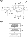
- FIG 2 shows an inventive source module 30, which corresponds to a source module 3, 17 of the projection exposure apparatus 1 described in figure 1 .
- the source module 30 comprises a collector mirror 31 with a recess 32.
- the recess 32 allows a laser beam 33 to irradiate onto a tin droplet 35 for generating an EUV-light 16 emitting plasma 34.
- the collector mirror 31 contains a reflective coating 37 on the optically active surface 38, which is the area of the collector mirror 31 used to reflect the emitted EUV-Light 16 from the plasma 34.
Landscapes
- Physics & Mathematics (AREA)
- General Physics & Mathematics (AREA)
- Optics & Photonics (AREA)
- Exposure Of Semiconductors, Excluding Electron Or Ion Beam Exposure (AREA)
- Exposure And Positioning Against Photoresist Photosensitive Materials (AREA)
Priority Applications (1)
| Application Number | Priority Date | Filing Date | Title |
|---|---|---|---|
| EP24166115.6A EP4530719A1 (fr) | 2024-03-26 | 2024-03-26 | Procédé d'optimisation de l'émission d'un rayonnement électromagnétique d'un plasma d'un système d'éclairage, module source, système d'éclairage, appareil d'exposition par projection |
Applications Claiming Priority (1)
| Application Number | Priority Date | Filing Date | Title |
|---|---|---|---|
| EP24166115.6A EP4530719A1 (fr) | 2024-03-26 | 2024-03-26 | Procédé d'optimisation de l'émission d'un rayonnement électromagnétique d'un plasma d'un système d'éclairage, module source, système d'éclairage, appareil d'exposition par projection |
Publications (1)
| Publication Number | Publication Date |
|---|---|
| EP4530719A1 true EP4530719A1 (fr) | 2025-04-02 |
Family
ID=90473386
Family Applications (1)
| Application Number | Title | Priority Date | Filing Date |
|---|---|---|---|
| EP24166115.6A Withdrawn EP4530719A1 (fr) | 2024-03-26 | 2024-03-26 | Procédé d'optimisation de l'émission d'un rayonnement électromagnétique d'un plasma d'un système d'éclairage, module source, système d'éclairage, appareil d'exposition par projection |
Country Status (1)
| Country | Link |
|---|---|
| EP (1) | EP4530719A1 (fr) |
Citations (14)
| Publication number | Priority date | Publication date | Assignee | Title |
|---|---|---|---|---|
| US6573978B1 (en) | 1999-01-26 | 2003-06-03 | Mcguire, Jr. James P. | EUV condenser with non-imaging optics |
| US20060132747A1 (en) | 2003-04-17 | 2006-06-22 | Carl Zeiss Smt Ag | Optical element for an illumination system |
| DE102008009600A1 (de) | 2008-02-15 | 2009-08-20 | Carl Zeiss Smt Ag | Facettenspiegel zum Einsatz in einer Projektionsbelichtungsanlage für die Mikro-Lithographie |
| DE102010063530A1 (de) * | 2009-12-22 | 2011-06-30 | Carl Zeiss SMT GmbH, 73447 | Blendenelement und optisches System für die EUV-Lithographie |
| US20180074303A1 (en) | 2015-04-14 | 2018-03-15 | Carl Zeiss Smt Gmbh | Imaging optical unit and projection exposure unit including same |
| DE102017220586A1 (de) | 2017-11-17 | 2019-05-23 | Carl Zeiss Smt Gmbh | Pupillenfacettenspiegel, Beleuchtungsoptik und optisches System für eine Projek-tionsbelichtungsanlage |
| US10429729B2 (en) | 2017-04-28 | 2019-10-01 | Taiwan Semiconductor Manufacturing Co., Ltd. | EUV radiation modification methods and systems |
| US20200018949A1 (en) | 2018-07-12 | 2020-01-16 | Triple Win Technology(Shenzhen) Co.Ltd. | Flare- and ghost-free imaging device |
| WO2020086901A1 (fr) * | 2018-10-26 | 2020-04-30 | Asml Netherlands B.V. | Surveillance des émissions de lumière |
| US20200348600A1 (en) * | 2018-01-31 | 2020-11-05 | Carl Zeiss Smt Gmbh | Illumination optic for projection lithography |
| US20220334472A1 (en) * | 2021-04-16 | 2022-10-20 | Taiwan Semiconductor Manufacturing Co., Ltd. | Lithography system and methods |
| WO2022244306A1 (fr) | 2021-05-17 | 2022-11-24 | ファナック株式会社 | Dispositif de discrimination vidéo, système de discrimination vidéo et support de stockage |
| US20230018949A1 (en) * | 2019-12-20 | 2023-01-19 | Asml Netherlands B.V. | Calibration system for an extreme ultraviolet light source |
| DE102022209573A1 (de) * | 2022-09-13 | 2023-11-23 | Carl Zeiss Smt Gmbh | EUV-Kollektor zur Verwendung in einer EUV-Projektionsbelichtungsvorrichtung |
-
2024
- 2024-03-26 EP EP24166115.6A patent/EP4530719A1/fr not_active Withdrawn
Patent Citations (15)
| Publication number | Priority date | Publication date | Assignee | Title |
|---|---|---|---|---|
| US6573978B1 (en) | 1999-01-26 | 2003-06-03 | Mcguire, Jr. James P. | EUV condenser with non-imaging optics |
| US20060132747A1 (en) | 2003-04-17 | 2006-06-22 | Carl Zeiss Smt Ag | Optical element for an illumination system |
| EP1614008B1 (fr) | 2003-04-17 | 2009-12-02 | Carl Zeiss SMT AG | Element optique pour systeme d eclairage |
| DE102008009600A1 (de) | 2008-02-15 | 2009-08-20 | Carl Zeiss Smt Ag | Facettenspiegel zum Einsatz in einer Projektionsbelichtungsanlage für die Mikro-Lithographie |
| DE102010063530A1 (de) * | 2009-12-22 | 2011-06-30 | Carl Zeiss SMT GmbH, 73447 | Blendenelement und optisches System für die EUV-Lithographie |
| US20180074303A1 (en) | 2015-04-14 | 2018-03-15 | Carl Zeiss Smt Gmbh | Imaging optical unit and projection exposure unit including same |
| US10429729B2 (en) | 2017-04-28 | 2019-10-01 | Taiwan Semiconductor Manufacturing Co., Ltd. | EUV radiation modification methods and systems |
| DE102017220586A1 (de) | 2017-11-17 | 2019-05-23 | Carl Zeiss Smt Gmbh | Pupillenfacettenspiegel, Beleuchtungsoptik und optisches System für eine Projek-tionsbelichtungsanlage |
| US20200348600A1 (en) * | 2018-01-31 | 2020-11-05 | Carl Zeiss Smt Gmbh | Illumination optic for projection lithography |
| US20200018949A1 (en) | 2018-07-12 | 2020-01-16 | Triple Win Technology(Shenzhen) Co.Ltd. | Flare- and ghost-free imaging device |
| WO2020086901A1 (fr) * | 2018-10-26 | 2020-04-30 | Asml Netherlands B.V. | Surveillance des émissions de lumière |
| US20230018949A1 (en) * | 2019-12-20 | 2023-01-19 | Asml Netherlands B.V. | Calibration system for an extreme ultraviolet light source |
| US20220334472A1 (en) * | 2021-04-16 | 2022-10-20 | Taiwan Semiconductor Manufacturing Co., Ltd. | Lithography system and methods |
| WO2022244306A1 (fr) | 2021-05-17 | 2022-11-24 | ファナック株式会社 | Dispositif de discrimination vidéo, système de discrimination vidéo et support de stockage |
| DE102022209573A1 (de) * | 2022-09-13 | 2023-11-23 | Carl Zeiss Smt Gmbh | EUV-Kollektor zur Verwendung in einer EUV-Projektionsbelichtungsvorrichtung |
Similar Documents
| Publication | Publication Date | Title |
|---|---|---|
| JP5888622B2 (ja) | マイクロリソグラフィ用の照明光学系 | |
| KR101373380B1 (ko) | 마이크로리소그래피 투영 노광 장치 및 그에 포함된 광학 표면에 관한 파라미터의 측정 방법 | |
| CN102349026B (zh) | 微光刻投射曝光设备 | |
| US9754695B2 (en) | EUV collector | |
| US12339589B2 (en) | Digital micromirror device for an illumination optical component of a projection exposure system | |
| US11350513B2 (en) | Stop for arrangement in a constriction of an EUV illumination beam | |
| US10928733B2 (en) | Illumination optic for projection lithography | |
| WO2022084066A1 (fr) | Appareil d'exposition par projection comprenant un dispositif de chauffage et un polariseur | |
| US20260036912A1 (en) | Lithography system and method for operating a lithography system | |
| US20250208521A1 (en) | Arrangement, method and computer program product for calibrating facet mirrors | |
| US20250147426A1 (en) | Facet mirror assembly | |
| US20260079336A1 (en) | Mems mirror, micromirror array and illumination system for a lithography system, lithography system, and method for producing a lithography system | |
| US20260023328A1 (en) | Lithography apparatus and method for operating a lithography apparatus | |
| WO2010112328A1 (fr) | Optique d'imagerie et installation d'exposition de projection pour la micro-lithographie avec une optique d'imagerie de ce type | |
| EP4530719A1 (fr) | Procédé d'optimisation de l'émission d'un rayonnement électromagnétique d'un plasma d'un système d'éclairage, module source, système d'éclairage, appareil d'exposition par projection | |
| WO2025073458A1 (fr) | Système de mesure, procédé de mesure utilisant un tel système de mesure, et appareil d'exposition par projection comprenant un tel système de mesure | |
| EP4625047A1 (fr) | Procédé d'optimisation de l'émission de rayonnement électromagnétique d'un système d'éclairage d'un appareil d'exposition par projection, système d'éclairage, appareil d'exposition par projection | |
| US20250199294A1 (en) | Method to adjust an illumination beam path within an illumination optics and illumination optics having an adjustment system | |
| US20250044703A1 (en) | Method for measuring an illumination angle distribution on an object field and illumination optics unit having an illumination channel allocation intended therefor | |
| NL2029213B1 (en) | Stop apparatus for delimiting a beam path between a light source and an illumination optical unit of a projection exposure apparatus for projection lithography | |
| US20250110413A1 (en) | Method for compensating actuator effects of actuators | |
| TWI918727B (zh) | 在用於投影微影之投影曝光設備的光源與照明光學單元之間限定射束路徑的光闌設備 | |
| US20250068078A1 (en) | Optical system, lithography apparatus having an optical system, and method for producing an optical system | |
| WO2024002672A1 (fr) | Collecteur de rayons euv pour appareil d'exposition par projection euv |
Legal Events
| Date | Code | Title | Description |
|---|---|---|---|
| PUAI | Public reference made under article 153(3) epc to a published international application that has entered the european phase |
Free format text: ORIGINAL CODE: 0009012 |
|
| STAA | Information on the status of an ep patent application or granted ep patent |
Free format text: STATUS: THE APPLICATION HAS BEEN PUBLISHED |
|
| AK | Designated contracting states |
Kind code of ref document: A1 Designated state(s): AL AT BE BG CH CY CZ DE DK EE ES FI FR GB GR HR HU IE IS IT LI LT LU LV MC ME MK MT NL NO PL PT RO RS SE SI SK SM TR |
|
| STAA | Information on the status of an ep patent application or granted ep patent |
Free format text: STATUS: THE APPLICATION HAS BEEN WITHDRAWN |
|
| 18W | Application withdrawn |
Effective date: 20250409 |