EP4530870A1 - Système et procédé de communication d'interface périphérique série - Google Patents
Système et procédé de communication d'interface périphérique série Download PDFInfo
- Publication number
- EP4530870A1 EP4530870A1 EP23200950.6A EP23200950A EP4530870A1 EP 4530870 A1 EP4530870 A1 EP 4530870A1 EP 23200950 A EP23200950 A EP 23200950A EP 4530870 A1 EP4530870 A1 EP 4530870A1
- Authority
- EP
- European Patent Office
- Prior art keywords
- slave device
- data
- read
- register address
- write
- Prior art date
- Legal status (The legal status is an assumption and is not a legal conclusion. Google has not performed a legal analysis and makes no representation as to the accuracy of the status listed.)
- Pending
Links
Images
Classifications
-
- G—PHYSICS
- G06—COMPUTING OR CALCULATING; COUNTING
- G06F—ELECTRIC DIGITAL DATA PROCESSING
- G06F13/00—Interconnection of, or transfer of information or other signals between, memories, input/output devices or central processing units
- G06F13/38—Information transfer, e.g. on bus
- G06F13/42—Bus transfer protocol, e.g. handshake; Synchronisation
- G06F13/4282—Bus transfer protocol, e.g. handshake; Synchronisation on a serial bus, e.g. I2C bus, SPI bus
- G06F13/4291—Bus transfer protocol, e.g. handshake; Synchronisation on a serial bus, e.g. I2C bus, SPI bus using a clocked protocol
-
- G—PHYSICS
- G06—COMPUTING OR CALCULATING; COUNTING
- G06F—ELECTRIC DIGITAL DATA PROCESSING
- G06F13/00—Interconnection of, or transfer of information or other signals between, memories, input/output devices or central processing units
- G06F13/38—Information transfer, e.g. on bus
- G06F13/42—Bus transfer protocol, e.g. handshake; Synchronisation
- G06F13/4282—Bus transfer protocol, e.g. handshake; Synchronisation on a serial bus, e.g. I2C bus, SPI bus
-
- G—PHYSICS
- G06—COMPUTING OR CALCULATING; COUNTING
- G06F—ELECTRIC DIGITAL DATA PROCESSING
- G06F9/00—Arrangements for program control, e.g. control units
- G06F9/06—Arrangements for program control, e.g. control units using stored programs, i.e. using an internal store of processing equipment to receive or retain programs
- G06F9/30—Arrangements for executing machine instructions, e.g. instruction decode
- G06F9/30003—Arrangements for executing specific machine instructions
- G06F9/3004—Arrangements for executing specific machine instructions to perform operations on memory
- G06F9/30043—LOAD or STORE instructions; Clear instruction
-
- G—PHYSICS
- G06—COMPUTING OR CALCULATING; COUNTING
- G06F—ELECTRIC DIGITAL DATA PROCESSING
- G06F9/00—Arrangements for program control, e.g. control units
- G06F9/06—Arrangements for program control, e.g. control units using stored programs, i.e. using an internal store of processing equipment to receive or retain programs
- G06F9/30—Arrangements for executing machine instructions, e.g. instruction decode
- G06F9/30098—Register arrangements
- G06F9/30141—Implementation provisions of register files, e.g. ports
-
- G—PHYSICS
- G06—COMPUTING OR CALCULATING; COUNTING
- G06F—ELECTRIC DIGITAL DATA PROCESSING
- G06F2213/00—Indexing scheme relating to interconnection of, or transfer of information or other signals between, memories, input/output devices or central processing units
- G06F2213/0002—Serial port, e.g. RS232C
Definitions
- the present disclosure relates to a method and system for serial data communication between a master device and one or more slave devices.
- a serial peripheral interface is a communication interface typically used for data communication between a master device (e.g., a computer and a microcontroller) and slave devices such as peripheral slave chips used in conjunction with peripheral devices (e.g., peripheral integrated circuits (ICs)) such as shift registers, sensors, analogue-to-digital converters (ADCs), digital-to-analogue converters (DACs) and memory devices.
- ICs peripheral integrated circuits
- ADCs analogue-to-digital converters
- DACs digital-to-analogue converters
- a conventional SPI interface uses 4-wires, where each wire transmits the following signals: serial clock (or clock signal); main out, subnode in (MOSI) for transmitting data from the main (i.e., master or controller device) to the subnode (i.e., a slave or peripheral device); main in, subnode out (MISO) for transmitting data from the subnode to the main; and a chip select line for selecting which peripheral to communicate with.
- serial clock or clock signal
- MOSI main out, subnode in
- MISO subnode out
- the master device establishes communication with the slave device using the chip select line. Once the communication has been established with the slave device, the master device transmits to the slaves a start register address (i.e., an address byte) that indicates from which slave register address the slave will start reading data for a read operation by the master, or from which slave register address the master will start writing data to the slave.
- a start register address i.e., an address byte
- the master device requests new data (or information) from the slave device, or write data to the slave device, on demand.
- the master device sends the read-address to the slave of the register it would like to read the data content from.
- the master device sends the write address to the slave of the register it would like to write the data content to.
- the slave sends back to the master device the data content which was requested, or confirmation that the data has been written to the slave.
- both the read and write requests are separate communications. Therefore, the master device needs to communicate twice (i.e., two communication cycles) with the slave device before both a read and write operation are performed.
- the present disclosure seeks to address the problems associated with conventional SPI communication, particularly reducing the number of communications between a master and a slave device.
- a method of peripheral interface, SPI, communication comprises the step of transmitting a data packet from the master device to a slave device.
- the master devices can be referred to as a controller and slave device can be referred to as peripheral device.
- the data packet comprising a read register address, a write register address, and write data.
- the read register address and the write register address corresponding to a data register of the plurality of data registers of the slave device.
- the method further comprises the step of receiving a portion of the data packet at the slave device.
- the portion of the data packet comprising the read register address.
- the method further comprises the step of reading the read register address in the data packet at the slave device.
- the method further comprises the step of transmitting, from the slave device, data from the data register corresponding to the read register address of the slave device to the master device after the read register address has been read.
- a master device can transmit both a read operation and a write operation in the same communication to a slave device.
- the number of data packets sent between the master device and slave device is minimised, which results in faster and more efficient communication between the master device and the slave device.
- the slave device sends the data to the master device before the master device transmits the whole data packet, which results in faster read operations.
- the slave device does not need to store information between subsequent communications as both the read and write operations are transmitting in one data packet.
- the method further comprises transmitting the read register address of the slave device to the master device. In this way, the master device is able to determine if the correct register was read at the slave device.
- the method further comprises reading the write register address at the slave device.
- the write register address corresponding to the data register of the plurality of data registers of the slave device for storing the write data.
- the method further comprising the step of storing the write data at the write register address of the slave device. In this way, write data (or any data to be written to the slave device) can be transmitted and then subsequently stored at the corresponding register of the slave device.
- a delay is provided between reading, at the slave device, the read register address of the slave device and transmitting, from the slave device, the data from the read register address of the slave device. In this way, the slave device transmits the data the master device needed in addition to the data being written to a register of the slave device.
- the delay corresponds with a length of the write register address transmitted by the master device.
- the length of the data packet transmitted from the slave device corresponds with the length of the data packet sent to the slave device.
- the delay provides sufficient time for the slave device to find, prepare and transmit the data to the master device.
- the data packet comprises parity data. In this way, every portion of the data packet can be verified to be correct.
- the read register address of the slave device transmitted to the master device comprises a read address parity check. In this way, the master device can verify if the correct read address has been received at the slave device and the data transmitted to the master device is the data requested.
- the method further comprises transmitting check data from the slave device to the master device. In this way, the slave device can verify that both the read and write operations have been successfully completed.
- transmitting the data from the slave device to the master device and transmitting the write data from the master device to the slave device occurs at the same time. In this way, information between the slave and master device can be transmitted at the same time providing more efficient communication and does not require additional communication cycles to transmit information between the master and slave devices.
- a serial peripheral interface, SPI, communication system comprising a master device and a slave device.
- the master device is configured to transmit a data packet to the slave device.
- the data packet comprising a read register address, a write register address, and write data.
- the read register address and the write register address correspond to a data register of the plurality of data registers of the slave device.
- the slave device is configured to receive and read a portion of the data packet comprising the read register address, and transmit data from the read register address of the slave device to the master device after the read register address has been read.
- the slave device is configured to transmit the read register address of the slave device to the master device.
- the slave device is configured to read the write register address, the write register address comprising a register location for the write data to be stored, and stores the write data at the write register address of the slave device.
- the slave device is configured to provide a delay between reading, at the slave device, the read register address of the slave device and transmitting, from the slave device, the data from the read register address of the slave device.
- the delay corresponds with a length of the write register address transmitted by the master device.
- the slave device is configured to transmit the data to the master device at the same time as the master device transmits the write data to the slave device.
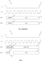
- FIG. 1 illustrates SPI communication 10 between a master device and a slave device (not shown).
- the SPI communication 10 occurs through four signal lines: a chip select (CS) line, a clock signal (CLK) line, a MOSI data line, and a MISO data line.
- the CS signal 11 is held at a high state on the CS line when serial data communication is not intended between the master device and the slave device. If the master device needs to communicate with a slave device, the CS signal 11 to said slave device is held at a low state during the serial data communication between the master device and the slave device. Alternatively, the high and low state can be reversed.
- slave devices can be connected to a master device, whereby the CS line is used to activate at least one of the slave devices that are connected to the master device such that serial data communication can occur between the master device and the selected slave device(s).
- the master device deactivates the CLK signal 12 and sets the CS signal 11 to a high state.
- the clock signal 12 is a periodic signal that synchronises the data transfer between the master and slave devices and is typically transmitted by the master device.
- the clock signal 12 determines the maximum data transfer rate and the bit timing of the data transfer.
- the slave device uses the clock signal 12 to determine when to receive data.
- the clock signal can first be transmitted in the high state or in the low state depending on the configuration of the master and slave device.
- the CS signal 11 is held at a low state and the master device transmits a clock signal 12 on the CLK line, SPI communication between the master device and slave device can occur.
- the master device transmits a data packet on the MOSI line to the slave device.
- the data packet comprises either a read or write address 13.
- the data packet comprises data 14, which comprises information to be written to the slave device at the write address 13, or the data comprises a read command 14 if the master devices need to read data from the read address of the slave device.
- the data packet is received at the slave device, which receives and reads the data packet according to the CLK signal 11.
- the slave device comprises a plurality of registers, each with a corresponding register address. Each register corresponds with a parameter stored by the slave device. For example, one such parameter can be a temperature reading that is stored at a register of the slave device.
- the master device needs to read data from a register of the slave device, the master device sends the read register address 13 of the register it needs to read data from.
- the data 14 comprises a read command, which indicates to the slave device that the master needs to read data from the slave device.
- the slave device copies the data from the register, corresponding with the transmitted read address, to an SPI transmit register before being transmitted to the master device. Once this has occurred, the slave device transmits a data packet back to the master device via the MISO line.
- the data packet comprising the read address 15 of the register from which the data was read and the data 16 from the SPI transmit register.
- the data packet is received at the master device, which receives and reads the data packet according to the CLK signal 11.
- the master device sends a write address 13 and write data 14 in the data packet on the MOSI line to the slave device.
- the write address 13 corresponding with the register of the slave device that data is to be written to.
- the data packet is received at the slave device, which receives and reads the data packet according to the CLK signal 11.
- the slave device stores the write data 14 at the register corresponding to the write address 13.
- the slave transmits a data packet back to the master device on the MISO line.
- the data packet comprising the write address 15 of the register of the slave device where the write data 14 was written to, and data 16 comprising a status code indicating if the operation was successful or unsuccessful.
- the master device must send two data packets (i.e., two separate messages) to transmit a read command and a write command.
- the read command and the write command occurs over two communication cycles which results in a delay in communication as the master device needs to send two messages before both commands (or operations) are completed.
- FIG. 2 shows SPI communication 20 between a master device and a slave device, according to the present disclosure, wherein a read and write command may be transmitted in one data packet (i.e., in one communication cycle).
- the master device transmits a data packet on the MOSI line to the slave device.
- the data packet comprising a read address 21, a write address 22 and write data 23.
- the read address 21 corresponding with a register of the slave device from which the master device needs to read from.
- the write address 22 corresponding with a register of the slave device from which the master device needs to write data to.
- the write data 23 comprising data to be written to the write address 22 corresponding with a data register of the slave device.
- the slave device receives the data packet and reads the information from the data packet. Once the slave device reads the read address 21 in the data packet from the master device, the slave device transmits a data packet to the master device with the read address 24 of the register from which the data 25 was read from and the data 25 contained at that particular read address 24 of the slave device.
- the transmission of the data packet to the master device is defined by the SPI clock.
- a delay 26 (corresponding to a time delay in CLK signal cycles) between the transmission of the read address 24 and the data 25 can be implemented, such that the slave device has sufficient time to receive and read the read address 21 and to prepare the data 25 at the read address 21 for transmission to the master device in the data packet.
- the delay 26 (or waiting time), could be according to cycles of CLK signal 12, or the delay 26 could correspond with the time taken (e.g., in cycles of CLK signal 12) for the master device to transmit the write address 22.
- the slave device does not transmit the data 25 to the master device within the delay 26.
- the slave device prepares the data by copying the relevant data to the slave device SPI data transmission register within the delay 26.
- the slave device sends the data 25 to the master device synchronously with the SPI clock (i.e., in the timeframe the master device sends the write data 23 to the slave device). Accordingly, the slave device transmits the data 25 to the master device once the read address 24 has been read and before the master device finishes sending the communication (i.e., the data packet).
- each of the read address 21, the write address 22, and the write data 23 can comprise parity data.
- the parity data comprising a parity bit, or a control bit, to ensure that the read address 21, the write address 22, and/or the write data 23 have not been corrupted during the communication process.
- each of the read address 24 and the data 25 can also include a parity bit or a control bit.
- the parity data can comprise a checksum. The checksum comprising one or more bits to verify data integrity.
- the slave device could send a confirmation bit (or an OK bit) at the end of the data packet.
- the confirmation bit can be transmitted by the slave device once the parity bit checks are successful and it has been verified that the correct data packet was transmitted to the master device.
- the confirmation bit provides confirmation to the master device that the communication was successful. If the confirmation bit is not sent by the slave device, the master device may resend the data packet as it may be assumed the previous communication was unsuccessful.
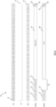
- Figure 3 shows an exemplary 64-bit SPI communication 30 between a master device and a slave device. Whilst Figure 3 shows 64-bit SPI communication 30, it is understood that SPI communication according to the present invention can occur using any of 8-bit, 16-bit and 32-bit SPI communication.
- the most significant bit 31 of the data packet is transmitted first to the slave device.
- the least significant bit of the data packet is transmitted first to the slave device.
- the read address 32 is the first portion of the data packet to be transmitted to the slave device, followed by a parity (P) bit 35 to ensure that the read address was transmitted and received correctly.
- the write address 33 and a corresponding parity bit 35 are transmitted to the slave device.
- the write data 34 and a parity bit 35 is sent to the slave device. Whilst a parity bit 35 has been described, it is possible for the parity bit 35 to be replaced or used in combination with a parity check.
- the parity check comprising at least one bit for verifying data integrity.
- the parity check can be a checksum.
- a DC bit 36, or data command bit 36 may be transmitted in the data packet to indicate the polarity of the data clock.
- the DC bit 36 when the DC bit 36 is high, the data on the MOSI line is interpreted as a command.
- the DC bit 36 is low, the data on the MOSI line is interpreted as data.
- the DC bit 36 can be transmitted first or last in the communication depending on the configuration of the master and slave device.
- the slave device transmits back the read address 37 to the master device on the MISO line.
- the read address 37 comprises a parity bit 35 to verify that the read address 37 was transmitted correctly.
- a delay 40 is initiated that corresponds with the length of time (e.g., in cycles of the CLK signal 12) it takes for the master device to transmit the write address 33 and the corresponding parity bit 35.
- the slave device transmits the data 38 from the read address 37 of the register of the slave device.
- the data 35 comprises a parity bit 35 and a confirmation bit 39.
- the master device needs to communicate only once with the slave device to write data to a register of the slave device and directly receive new information from the read address of the slave device.
- the master device receives confirmation by way of the confirmation bit 39 that both the read and write operation was successful.
Landscapes
- Engineering & Computer Science (AREA)
- Theoretical Computer Science (AREA)
- Physics & Mathematics (AREA)
- General Engineering & Computer Science (AREA)
- General Physics & Mathematics (AREA)
- Software Systems (AREA)
- Communication Control (AREA)
- Information Transfer Systems (AREA)
Priority Applications (3)
| Application Number | Priority Date | Filing Date | Title |
|---|---|---|---|
| EP23200950.6A EP4530870A1 (fr) | 2023-09-29 | 2023-09-29 | Système et procédé de communication d'interface périphérique série |
| CN202411313064.7A CN119739663A (zh) | 2023-09-29 | 2024-09-20 | 串行外围接口通信系统和方法 |
| US18/894,397 US20250110914A1 (en) | 2023-09-29 | 2024-09-24 | Serial Peripheral Interface Communication System and Method |
Applications Claiming Priority (1)
| Application Number | Priority Date | Filing Date | Title |
|---|---|---|---|
| EP23200950.6A EP4530870A1 (fr) | 2023-09-29 | 2023-09-29 | Système et procédé de communication d'interface périphérique série |
Publications (1)
| Publication Number | Publication Date |
|---|---|
| EP4530870A1 true EP4530870A1 (fr) | 2025-04-02 |
Family
ID=88237657
Family Applications (1)
| Application Number | Title | Priority Date | Filing Date |
|---|---|---|---|
| EP23200950.6A Pending EP4530870A1 (fr) | 2023-09-29 | 2023-09-29 | Système et procédé de communication d'interface périphérique série |
Country Status (3)
| Country | Link |
|---|---|
| US (1) | US20250110914A1 (fr) |
| EP (1) | EP4530870A1 (fr) |
| CN (1) | CN119739663A (fr) |
Citations (3)
| Publication number | Priority date | Publication date | Assignee | Title |
|---|---|---|---|---|
| US20080126638A1 (en) * | 2006-09-08 | 2008-05-29 | Samsung Electronics Co., Ltd. | Electronic apparatus with device capable of simultaneously reading and writing and method thereof |
| US20210280222A1 (en) * | 2020-03-06 | 2021-09-09 | Macronix International Co., Ltd. | Method and system for enhanced read performance in low pin count interface |
| US20220327092A1 (en) * | 2021-04-08 | 2022-10-13 | Infineon Technologies Ag | Serial data communication with in-frame response |
Family Cites Families (2)
| Publication number | Priority date | Publication date | Assignee | Title |
|---|---|---|---|---|
| US5566353A (en) * | 1994-09-06 | 1996-10-15 | Bylon Company Limited | Point of purchase video distribution system |
| CN102023945B (zh) * | 2009-09-22 | 2012-03-28 | 鸿富锦精密工业(深圳)有限公司 | 基于串行外围设备接口总线的设备及其数据传输方法 |
-
2023
- 2023-09-29 EP EP23200950.6A patent/EP4530870A1/fr active Pending
-
2024
- 2024-09-20 CN CN202411313064.7A patent/CN119739663A/zh active Pending
- 2024-09-24 US US18/894,397 patent/US20250110914A1/en active Pending
Patent Citations (3)
| Publication number | Priority date | Publication date | Assignee | Title |
|---|---|---|---|---|
| US20080126638A1 (en) * | 2006-09-08 | 2008-05-29 | Samsung Electronics Co., Ltd. | Electronic apparatus with device capable of simultaneously reading and writing and method thereof |
| US20210280222A1 (en) * | 2020-03-06 | 2021-09-09 | Macronix International Co., Ltd. | Method and system for enhanced read performance in low pin count interface |
| US20220327092A1 (en) * | 2021-04-08 | 2022-10-13 | Infineon Technologies Ag | Serial data communication with in-frame response |
Also Published As
| Publication number | Publication date |
|---|---|
| CN119739663A (zh) | 2025-04-01 |
| US20250110914A1 (en) | 2025-04-03 |
Similar Documents
| Publication | Publication Date | Title |
|---|---|---|
| US6173355B1 (en) | System for sending and receiving data on a universal serial bus (USB) using a memory shared among a number of endpoints | |
| JP4966695B2 (ja) | マルチマスタのチェーン接続された二線シリアルバス装置及びディジタル状態機械 | |
| CN107832250B (zh) | 一种基于spi的主从通讯时序方法 | |
| CN100440187C (zh) | 经由i2c总线随机访问设备中的单元的方法 | |
| KR19990067731A (ko) | 유니버설 시리얼 버스 제어 이전을 처리하는 장치 및 방법 | |
| US8185680B2 (en) | Method for changing ownership of a bus between master/slave devices | |
| JPH09128330A (ja) | 映像表示装置 | |
| US20220188254A1 (en) | Methods for identifying target slave address for serial communication interface | |
| US6070208A (en) | Apparatus and method for implementing a versatile USB endpoint pipe | |
| US6931468B2 (en) | Method and apparatus for addressing multiple devices simultaneously over a data bus | |
| US20070088874A1 (en) | Offload engine as processor peripheral | |
| EP4530870A1 (fr) | Système et procédé de communication d'interface périphérique série | |
| JP3703532B2 (ja) | 多重化アドレスバスを備えたコンピュータシステム | |
| JPS59106021A (ja) | バス構成方式 | |
| US20250370953A1 (en) | Serial bus system | |
| JPH02262747A (ja) | データ通信方法 | |
| US20050144331A1 (en) | On-chip serialized peripheral bus system and operating method thereof | |
| CN113474762A (zh) | 在i2c总线之上的链接数据的传输 | |
| JP2578773B2 (ja) | シリアルデ−タ転送装置 | |
| CN114880270B (zh) | Spi设备及其数据传输方法 | |
| JPS63228856A (ja) | 通信制御装置 | |
| KR100295683B1 (ko) | 인터아이씨의 제너럴콜 어크날리지장치및 방법 | |
| JPH10207834A (ja) | シリアル入出力回路 | |
| KR0154470B1 (ko) | 보조제어장치와 외부장치간 정합회로 | |
| CN121966776A (zh) | 同步串行通信系统和方法 |
Legal Events
| Date | Code | Title | Description |
|---|---|---|---|
| PUAI | Public reference made under article 153(3) epc to a published international application that has entered the european phase |
Free format text: ORIGINAL CODE: 0009012 |
|
| STAA | Information on the status of an ep patent application or granted ep patent |
Free format text: STATUS: THE APPLICATION HAS BEEN PUBLISHED |
|
| AK | Designated contracting states |
Kind code of ref document: A1 Designated state(s): AL AT BE BG CH CY CZ DE DK EE ES FI FR GB GR HR HU IE IS IT LI LT LU LV MC ME MK MT NL NO PL PT RO RS SE SI SK SM TR |
|
| STAA | Information on the status of an ep patent application or granted ep patent |
Free format text: STATUS: REQUEST FOR EXAMINATION WAS MADE |
|
| 17P | Request for examination filed |
Effective date: 20250811 |
|
| GRAP | Despatch of communication of intention to grant a patent |
Free format text: ORIGINAL CODE: EPIDOSNIGR1 |
|
| STAA | Information on the status of an ep patent application or granted ep patent |
Free format text: STATUS: GRANT OF PATENT IS INTENDED |
|
| GRAJ | Information related to disapproval of communication of intention to grant by the applicant or resumption of examination proceedings by the epo deleted |
Free format text: ORIGINAL CODE: EPIDOSDIGR1 |
|
| STAA | Information on the status of an ep patent application or granted ep patent |
Free format text: STATUS: REQUEST FOR EXAMINATION WAS MADE |
|
| GRAP | Despatch of communication of intention to grant a patent |
Free format text: ORIGINAL CODE: EPIDOSNIGR1 |
|
| STAA | Information on the status of an ep patent application or granted ep patent |
Free format text: STATUS: GRANT OF PATENT IS INTENDED |