EP4531084A1 - Ensemble et système de support - Google Patents
Ensemble et système de support Download PDFInfo
- Publication number
- EP4531084A1 EP4531084A1 EP23201001.7A EP23201001A EP4531084A1 EP 4531084 A1 EP4531084 A1 EP 4531084A1 EP 23201001 A EP23201001 A EP 23201001A EP 4531084 A1 EP4531084 A1 EP 4531084A1
- Authority
- EP
- European Patent Office
- Prior art keywords
- wafer
- positioning
- carrier
- tilting mechanism
- assembly
- Prior art date
- Legal status (The legal status is an assumption and is not a legal conclusion. Google has not performed a legal analysis and makes no representation as to the accuracy of the status listed.)
- Pending
Links
Images



Classifications
-
- H—ELECTRICITY
- H10—SEMICONDUCTOR DEVICES; ELECTRIC SOLID-STATE DEVICES NOT OTHERWISE PROVIDED FOR
- H10P—GENERIC PROCESSES OR APPARATUS FOR THE MANUFACTURE OR TREATMENT OF DEVICES COVERED BY CLASS H10
- H10P72/00—Handling or holding of wafers, substrates or devices during manufacture or treatment thereof
- H10P72/70—Handling or holding of wafers, substrates or devices during manufacture or treatment thereof for supporting or gripping
- H10P72/76—Handling or holding of wafers, substrates or devices during manufacture or treatment thereof for supporting or gripping using mechanical means, e.g. clamps or pinches
- H10P72/7604—Handling or holding of wafers, substrates or devices during manufacture or treatment thereof for supporting or gripping using mechanical means, e.g. clamps or pinches the wafers being placed on a susceptor, stage or support
- H10P72/7611—Handling or holding of wafers, substrates or devices during manufacture or treatment thereof for supporting or gripping using mechanical means, e.g. clamps or pinches the wafers being placed on a susceptor, stage or support characterised by edge profile or support profile
-
- H—ELECTRICITY
- H10—SEMICONDUCTOR DEVICES; ELECTRIC SOLID-STATE DEVICES NOT OTHERWISE PROVIDED FOR
- H10P—GENERIC PROCESSES OR APPARATUS FOR THE MANUFACTURE OR TREATMENT OF DEVICES COVERED BY CLASS H10
- H10P72/00—Handling or holding of wafers, substrates or devices during manufacture or treatment thereof
- H10P72/70—Handling or holding of wafers, substrates or devices during manufacture or treatment thereof for supporting or gripping
- H10P72/76—Handling or holding of wafers, substrates or devices during manufacture or treatment thereof for supporting or gripping using mechanical means, e.g. clamps or pinches
- H10P72/7604—Handling or holding of wafers, substrates or devices during manufacture or treatment thereof for supporting or gripping using mechanical means, e.g. clamps or pinches the wafers being placed on a susceptor, stage or support
- H10P72/7606—Handling or holding of wafers, substrates or devices during manufacture or treatment thereof for supporting or gripping using mechanical means, e.g. clamps or pinches the wafers being placed on a susceptor, stage or support characterised by edge clamping, e.g. clamping ring
-
- H—ELECTRICITY
- H10—SEMICONDUCTOR DEVICES; ELECTRIC SOLID-STATE DEVICES NOT OTHERWISE PROVIDED FOR
- H10P—GENERIC PROCESSES OR APPARATUS FOR THE MANUFACTURE OR TREATMENT OF DEVICES COVERED BY CLASS H10
- H10P72/00—Handling or holding of wafers, substrates or devices during manufacture or treatment thereof
- H10P72/70—Handling or holding of wafers, substrates or devices during manufacture or treatment thereof for supporting or gripping
- H10P72/76—Handling or holding of wafers, substrates or devices during manufacture or treatment thereof for supporting or gripping using mechanical means, e.g. clamps or pinches
- H10P72/7604—Handling or holding of wafers, substrates or devices during manufacture or treatment thereof for supporting or gripping using mechanical means, e.g. clamps or pinches the wafers being placed on a susceptor, stage or support
- H10P72/7608—Handling or holding of wafers, substrates or devices during manufacture or treatment thereof for supporting or gripping using mechanical means, e.g. clamps or pinches the wafers being placed on a susceptor, stage or support characterised by a plurality of separate clamping members, e.g. clamping fingers
-
- H—ELECTRICITY
- H10—SEMICONDUCTOR DEVICES; ELECTRIC SOLID-STATE DEVICES NOT OTHERWISE PROVIDED FOR
- H10P—GENERIC PROCESSES OR APPARATUS FOR THE MANUFACTURE OR TREATMENT OF DEVICES COVERED BY CLASS H10
- H10P72/00—Handling or holding of wafers, substrates or devices during manufacture or treatment thereof
- H10P72/70—Handling or holding of wafers, substrates or devices during manufacture or treatment thereof for supporting or gripping
- H10P72/76—Handling or holding of wafers, substrates or devices during manufacture or treatment thereof for supporting or gripping using mechanical means, e.g. clamps or pinches
- H10P72/7604—Handling or holding of wafers, substrates or devices during manufacture or treatment thereof for supporting or gripping using mechanical means, e.g. clamps or pinches the wafers being placed on a susceptor, stage or support
- H10P72/7624—Handling or holding of wafers, substrates or devices during manufacture or treatment thereof for supporting or gripping using mechanical means, e.g. clamps or pinches the wafers being placed on a susceptor, stage or support characterised by the mechanical construction of the susceptor, stage or support
Definitions
- the processability of the wafers is limited because the carrier assemblies known from the prior art either partially cover the wafer, so that the wafer can only be processed on one side, or parts of the outer edge of the wafer are covered, whereby the surface available for processing is limited compared to the entire surface of the wafer.
- the wafer is held or clamped within the carrier using complex mechanisms that require a correspondingly large amount of space. This reduces the efficiency of fully automated processing because the number of wafers that can be processed simultaneously is limited.
- the object of the invention is to provide a carrier assembly that enables fully automated processing of the wafer while maximizing processing efficiency.
- the object is achieved according to the invention by a carrier assembly for the play-free positioning of a wafer.
- the carrier assembly comprises a carrier for the wafer, a tilting mechanism, and a positioning part.
- the carrier has an opening for receiving the wafer.
- the positioning part has a positioning surface for laterally positioning the wafer.
- the tilting mechanism is configured to tilt the positioning part between a release position and a positioning position in which the wafer is positioned between an edge of the opening and the positioning surface.
- the basic idea of the invention is to enable repeatable wafer positioning using the carrier assembly by positioning the wafer in the carrier using the positioning surface of the positioning part.
- This (exactly) defines the position of the wafer within the carrier, ensuring repeatability of the positioning. In other words, it is ensured that all wafers inserted in the carrier assembly are positioned in the same way.
- the positioning part ensures that the wafer remains in its specified position, even if the carrier assembly is subject to (light) vibrations that can occur, for example, in a process line, i.e., in a (fully) automated system. In this respect, the wafer can be positioned play-free during measurement, transport, and processing in a vacuum chamber.
- the tilting mechanism ensures that the carrier assembly is suitable for fully automated processing, as the tilting mechanism can be operated both manually and automatically, for example, via a trigger element that interacts with the tilting mechanism.
- the positioning part positions the wafer laterally by means of the positioning surface, it is also ensured that the surface of the wafer to be processed is not (partially) covered by the positioning part, as would be the case, for example, with a hold-down device that contacts a surface of the wafer to hold the wafer down.
- the tilting mechanism has at least one actuating surface via which the tilting mechanism can be actuated to tilt the positioning part between the positioning position and the release position.
- the actuating surface In the positioning position of the positioning part, the actuating surface is perpendicular to the positioning surface.
- the tilting mechanism ensures that the direction of force action changes by 90°, since the tilting mechanism is triggered from above or below by actuating the actuating surface, which results in a lateral force on the wafer, which is applied to the wafer via the positioning surface of the positioning part.
- the reversal of direction is realized by tilting the positioning part using the tilting mechanism.
- the actuation direction of the tilting mechanism i.e. the direction in which the tilting mechanism is triggered, is therefore parallel to the loading and unloading direction of the wafer.
- the tilting mechanism may comprise an actuating part which is mechanically connected to the positioning part, wherein the actuating surface on the Actuating part is formed.
- actuating part which is mechanically connected to the positioning part, wherein the actuating surface on the Actuating part is formed.
- the positioning part which is in direct contact with the wafer via its positioning surface, can be made of a different material than the actuating part, which is not in direct contact with the wafer. This allows for a more cost-effective carrier assembly.
- the positioning part is made of an ion beam-resistant material, such as graphite or PTFE.
- ion beam-resistant material such as graphite or PTFE.
- the components that contact the wafer are made of the ion beam-resistant material.
- Such a material is also suitable for (ultra-)high vacuum applications.
- the actuating part can be made of a metal, for example aluminum, so that it is as light as possible yet stable, thereby reducing the overall weight of the support assembly.
- the positioning part itself can also have the actuating surface, so that instead of two separate parts, a single, integral component is provided that simultaneously performs the functions of both the positioning part and the actuating part.
- this single-piece component would be intended for both the lateral positioning of the wafer and the actuation of the tilting mechanism.
- the tilting mechanism has at least one bearing block that defines a pivot point for the actuating part.
- the bearing block can be made of a PTFE material, making it suitable for (ultra-)high vacuum applications.
- a locating pin can be arranged in the bearing block, which defines a pivot axis of the tilting mechanism. In this respect, the pivot point for the actuating part is predetermined by the bearing block or the locating pin inserted in the bearing block.
- the carrier to have a recess at the edge through which the tilting mechanism partially extends.
- the tilting mechanism runs partially parallel to the loading or unloading line. Removal direction through the edge-side recess.
- the edge-side recess ensures that the tilting mechanism does not protrude laterally beyond the edge of the carrier. This ensures, among other things, that multiple carrier assemblies can be placed side by side on a multi-carrier, thus maximizing the number of carrier assemblies per multi-carrier. This, in turn, increases processing efficiency, as multiple wafers can be processed simultaneously.
- the tilting mechanism can be positioned laterally spaced from the opening in a plan view of the opening such that a wafer held in the carrier is accessible from two opposite sides.
- the two sides correspond to the top and bottom of the wafer, so that the wafer surfaces intended for processing are both accessible, in particular completely accessible.
- “Completely accessible” here means that a maximum of 1 to 2 mm of a wafer surface is concealed, i.e., a corresponding edge of the bottom or top.
- both sides of the carrier are thus (fully) accessible, allowing one side to be processed, for example, exposed to ion radiation, while cooling occurs simultaneously on the opposite side.
- the bottom of the wafer is irradiated with ions, whereas the top of the wafer is cooled.
- a cooling device can be brought closer to the side to be cooled for this purpose. Complicated cooling, as is the case in the prior art, can therefore be eliminated.
- a spring can be provided which interacts with the tilting mechanism in such a way that the positioning part is pre-tensioned in the positioning position. If the tilting mechanism is not actuated, the positioning part is in the positioning position in which an inserted wafer would be fixed in terms of its position. If there is no wafer in the carrier, loading is only possible if the tilting mechanism is actuated. In other words, insertion of the wafer or loading of the carrier can be prevented unless the tilting mechanism is actuated at the same time to transfer the positioning part from the positioning position to the release position.
- the spring can Support the carrier, in particular be arranged between the carrier and the actuating part.
- the positioning part is a clamping part having a clamping surface for laterally clamping the wafer, wherein the tilting mechanism is configured to tilt the clamping part between the release position and a clamping position in which the wafer is clamped between an edge of the opening and the clamping surface.
- a clamping contour is formed on an inner side of the carrier, which is opposite the clamping surface.
- the positioning or clamping surface can be adapted to the contour of the wafer, resulting in a flat contact area in the area of the positioning or clamping surface.
- the positioning or clamping surface can be partially circular, provided the positioning or clamping part comes into lateral contact in the area of a circular section of the wafer.
- the positioning or clamping part can be used in the area of a notch or flat of the wafer, whereby the positioning or clamping surface has a shape adapted to the notch or flat. If the positioning or clamping part is used in the area of a notch or flat, it can simultaneously ensure anti-twist protection, since the wafer can only be inserted into the carrier in a specific position.
- a further aspect provides that at least one support for an edge of the wafer is provided at the edge of the opening.
- the at least one support is interrupted in an area in which the positioning part is arranged.
- the support can be provided entirely at the edge of the opening, except for the interruption in the area of the positioning part.
- the at least one support thus corresponds to an inwardly projecting collar on which the edge of the wafer can be placed.
- several supports are provided which extend over segments of the edge of the opening, for example three segments or four segments. In any case, it is ensured that no segment is provided in the area of the positioning part which, via its positioning surface, laterally contacts the edge of the wafer in order to determine the position of the wafer in the carrier.
- the support can have a length
- the length of at least one support is a maximum of 2 mm.
- the support extends a maximum of 2 mm toward the center of the opening.
- the length is 1 mm. This results in a maximum coverage of the wafer edge of up to 2 mm, namely the length of the support. If multiple segmented supports are provided, the total covered area can be reduced accordingly.
- an adapter ring can be provided into which the carrier is inserted.
- the adapter ring can be made of a different material than the carrier, for example a metal such as aluminum. This ensures that the outside of the carrier assembly is made of a more stable material or one that is better suited for handling.
- the adapter ring can be made of a cheaper material than the carrier, thereby reducing overall costs. The different material selection is possible in particular because the adapter ring itself does not come into contact with the wafer, meaning that the adapter ring does not have to meet lower requirements than the carrier, which is also exposed to corresponding conditions during wafer processing.
- the invention provides a system with a gripping unit and a carrier assembly of the aforementioned type.
- the gripping unit is provided to load the carrier assembly with the wafer or to remove the wafer from the carrier assembly.
- the gripping unit can be a manual gripping unit, for example, a vacuum tweezers.
- the tilting mechanism can be triggered manually, for example by An operator pressing the actuation surface.
- the operator can hold the vacuum tweezers, the manually operated gripping unit, to insert the wafer into the carrier of the carrier assembly or remove the wafer from the carrier assembly.
- the gripping unit can be an automated gripping unit, for example, in the form of a robot's end effector.
- the tilting mechanism can be automatically triggered when the automated gripping unit inserts the wafer into or removes it from the carrier assembly.
- the gripping unit could be a vacuum gripper, which uses negative pressure to hold the wafer in position relative to the gripping unit during handling, a Bernoulli gripper, also known as a flow gripper, or an electrostatic gripper.
- a vacuum gripper which uses negative pressure to hold the wafer in position relative to the gripping unit during handling
- a Bernoulli gripper also known as a flow gripper
- an electrostatic gripper Other types of grippers that are equally suitable can of course also be used.
- the gripping unit has a trigger element that is configured to actuate the tilting mechanism, wherein the gripping unit is movable at least along a loading and unloading direction.
- the loading and unloading direction is parallel to an actuation direction of the tilting mechanism of the carrier assembly.
- the release element can be pin-shaped and arranged laterally adjacent to a suction device of the gripping unit, by means of which the wafer is held.
- the release element actuates the tilting mechanism from a certain distance from the carrier, whereby the positioning part is tilted into the release position so that the gripping unit can insert the carrier.
- the vacuum applied to the suction device is removed, releasing the wafer.
- the gripping unit is then moved to its starting position, causing the trigger element to release the tilting mechanism, which is then reset by the spring preload. This causes the positioning part to move into the positioning position, in which it positions the wafer laterally, thus securing the wafer's position within the carrier without any play.
- the tilting mechanism is actuated in a similar way when removing the wafer from the carrier using the gripping unit.
- the gripping unit is moved along the removal direction to contact the wafer.
- the trigger element has previously actuated the tilting mechanism, tilting the positioning part into the release position, which allows the gripping unit to remove the wafer from the carrier.
- the gripping unit can then contact the wafer via the suction device and hold it in place using negative pressure to remove the wafer.
- the trigger element is designed to be spring-loaded, which provides additional travel for the gripping unit. This ensures that the trigger element first actuates the tilting mechanism, in particular the suction device of the gripping unit, before the gripping unit even comes into contact with the wafer during removal. After the tilting mechanism has been triggered, the gripping unit is moved further in the direction of the wafer by means of the trigger element, so that the trigger element compresses. This ensures the additional travel for the gripping unit. This occurs in a similar way during loading, as here too the trigger element compresses and thus ensures additional travel for the gripping unit, so that the gripping unit, in particular its suction device, can be moved further in the loading direction in order to place the wafer on the at least one support.
- the spring travel of the trigger element can be adjusted to ensure that the gripping unit does not damage the wafer during removal or insertion, since, for example, a progressive spring characteristic is provided, which prevents the gripping unit from being moved too far in the loading direction. This provides additional safety in case the gripping unit is moved too far by the robot.
- the trigger element has a greater spring strength than the tilting mechanism, so that it is ensured that when the trigger element is contacted, the tilting mechanism is actuated first, i.e. the spring of the tilting mechanism is compressed in order to tilt the positioning part into the release position, before the trigger element compresses or a spring assigned to the trigger element is compressed.
- the tilting mechanism can be actuated via the trigger element, which is part of the gripping unit, provided that an automated process is provided that includes an automated gripping unit. If manual loading or unloading is provided, the tilting mechanism can also be manually actuated by the operator's hand, thereby tilting the positioning part into the release position.
- the tilting mechanism provides for lateral fixing of the wafer in the carrier.
- the tilting mechanism is actuated in a direction perpendicular to this.
- the carrier assembly is loaded from above, so that the wafer is inserted into the carrier assembly from above.
- at least one support for the wafer is provided on the edge of the opening in the carrier, onto which the wafer can be placed during insertion.
- the exact positioning of the wafer within the carrier is then carried out by means of the positioning part, which positions the wafer laterally in the support plane spanned by the at least one support so that its position is free of play. This accordingly fixes the position of the wafer in the carrier.
- the positioning part is designed in particular as a clamping part so that the wafer is clamped.
- the tilting mechanism also ensures that both sides of the wafer—the bottom and top—are fully accessible during processing. This allows the bottom of the wafer to be treated, for example, by ion irradiation, while the wafer is simultaneously cooled via the top.
- the actuating surface in particular the entire actuating part, can be arranged above the support and/or the adapter ring in a plan view of the support assembly.
- the opening is not covered by the actuating part.
- the actuating part also does not protrude laterally. This results in a compact design of the entire support assembly.
- the wafer can comprise a coated or uncoated semiconductor substrate, glass and/or ceramic, or mixtures of the aforementioned materials.
- FIG. 1 a system 10 is shown which is configured to process, for example, irradiate, several wafers simultaneously.
- the system 10 comprises a loading station 12, an adjoining irradiation station 14 and a measuring station 16.
- the measuring station 16 can be a removal station is connected, which essentially corresponds to that of the loading station 12.
- the system 10 can also comprise further measuring stations.
- a robot 18 is provided which loads a multiple carrier 20 with a plurality of wafers 22 which are inserted into carrier assemblies 24, as will be explained in detail below.
- the multiple carrier 20 can therefore comprise several carrier assemblies 24, for example eight carrier assemblies 24, so that several wafers 22 can be irradiated simultaneously in the irradiation station 14.
- the system 10 therefore represents a process line that ensures that the wafers 22 can be processed in the desired manner. This is made possible by the carrier assembly 24 holding the corresponding wafer 22 in a precise position during the process line. It is therefore not necessary for the wafer 22 to be removed from the carrier assembly 24 and repositioned.
- the carrier assembly 24 ensures repeatability because the wafer 22 is positioned in the carrier assembly 24 without play. This play-free positioning ensures that no displacement or repositioning of the wafer 22 occurs during transport of the wafer 22 through the multiple stations of the system 10, which would have a negative impact on its processing.
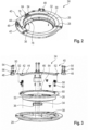
- the carrier assembly 24 comprises a carrier 26, which is received as an insert in an adapter ring 28.
- the adapter ring 28 can have a support surface 29 on which the carrier 26 rests.
- the carrier 26 has an opening 30 through which the wafer 22 can be inserted into the carrier 26. At the edge of the opening 30, the carrier 26 also has at least one support 32 onto which the wafer 22 can be placed with an edge of the underside when the wafer 22 is inserted into the carrier 26.
- the at least one support 32 is therefore an inwardly projecting projection or collar onto which the wafer 22 can be placed.
- the support 32 can project up to 2 millimeters.
- the carrier assembly 24 comprises a positioning part 34 which has a positioning surface 36 which is provided for laterally positioning the wafer 22 in the carrier 26.
- the positioning part 34 is arranged in an inwardly facing recess 38 of the carrier 26, as can be seen, inter alia, from the Figures 3 , 5 and 7 emerges.
- the positioning part 34 is operable with a tilting mechanism 40, whereby the positioning part 34 can be tilted between a release position and a positioning position in which the wafer 22 is positioned between an edge of the opening 30 and the positioning surface 36. In other words, in the positioning position, the position of the wafer 22 in the carrier assembly 24 or in the carrier 26 is fixed.
- the support 32 is interrupted in the area of the positioning part 34 so that the positioning part 34 can tilt and contact the wafer 22 laterally.
- the tilting mechanism 40 comprises an actuating surface 42 formed on the upper side of an actuating part 44, which is mechanically coupled to the positioning part 34.
- the actuating part 44 and the positioning part 34 are two separate components that are connected to one another. The connection can be made directly or, as in the embodiment shown, by means of a spacer element 46.
- a one-piece component is provided on which both the positioning surface 36 and the actuating surface 42 are provided. This one-piece component would therefore jointly perform the functions of the positioning part 34, the actuating part 44, and the spacer element 46.
- the tilting mechanism 40 also includes at least one bearing block 48, which defines a pivot point for the actuating part 44.
- the bearing block 48 has a receptacle 50 for a dowel pin 52, which in turn engages with a receptacle of the actuating part 44, thereby creating a pivot axis S for the actuating part 44.
- the actuating part 44 can be pivoted or tilted about the pivot axis S.
- the tilting mechanism 40 comprises two bearing blocks 48 which are designed in the same way.
- the at least one bearing block 48 is mechanically connected to the adapter ring 28 by means of screws 54 and optional springs 56.
- the tilting mechanism 40 comprises at least one spring 58, for example a compression spring.
- the spring 58 is provided to preload the tilting mechanism 40 or the positioning part 34 into the positioning position.
- the spring 58 in the embodiment shown rests on the support 26 to press the associated end of the actuating part 44, thereby initiating a pivoting movement about the pivot axis, which forces the positioning part 34 into the positioning position.
- the spring 58 is accommodated in a receptacle 60 in the support 26 together with an optional cylindrical pin 62.
- the carrier 26 has a peripheral recess 64 through which the tilting mechanism 40 extends at least partially, in particular the spacer element 46.
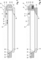
- the edge-side recess 64 is provided, among other things, on a collar 65 of the upper side of the carrier 26, so that the spacer element 46 can extend between the carrier 26 and the adapter ring 28, as can be seen from Figure 7 This creates a compact tilting mechanism 40 that allows multiple support assemblies 24 to be arranged side by side in the multiple support 20, thus ensuring maximum space efficiency.
- the carrier 26 can rest on the adapter ring 28 via the collar 65, in particular the support surface 29.
- the tilting mechanism 40 in a plan view of the opening 30 in the carrier 26, is provided at a distance from the opening 30 such that a wafer 22 accommodated in the carrier 26 is (fully) accessible from two opposite sides, as is clear from the figures.
- the wafer 22 can therefore be irradiated from below and simultaneously cooled from above by inserting a cooling device into the carrier assembly 24.
- the carrier 26 can have a contact surface 66 for the cooling device, so that the cooling device is arranged in a defined manner with respect to the wafer 22 accommodated in the carrier 26. This ensures that the cooling device does not directly contact the wafer 22, in particular its upper side, but maintains a defined distance therefrom.
- Figure 8 an alternative embodiment is shown which differs with regard to the tilting mechanism 40 from that shown in the Figures 2 to 7 shown embodiment.
- the one shown in Figure 8 shown embodiment of the carrier assembly 24 with regard to the positioning of the spring 58 in that the latter is supported on the adapter ring 28 and acts on the spacer element 46 in such a way that the positioning part 34 is pretensioned into the positioning position.
- an actuating part 44 is again provided which can be pivoted or tilted about the pivot axis S, which in the present case is defined by at least one knife edge 67, with which the actuating part 44 is supported on a component of the carrier assembly 24, for example the adapter ring 28.
- system 10 comprises a gripping unit 68, which can be used, for example, as an end effector of the robot 18 in the Figure 1 shown system 10 can be provided.
- the gripping unit 68 comprises, in addition to a suction device 70 with which the wafer 22 can be held, a trigger element 72 which is provided laterally spaced from the suction device 70, in particular on a flange 74.
- the trigger element 72 is resilient and is provided for triggering or actuating the tilting mechanism 40, so that the trigger element 72 interacts with the actuating surface 42 when the wafer 22 is introduced into the carrier assembly 24, as shown in Figures 9 and 10 shown, or removed from the carrier assembly 24.
- the gripping unit 68 is moved along a loading direction R parallel to an actuating direction B of the tilting mechanism 40 until the trigger element 72 contacts the actuating surface 42 and is adjusted against the spring preload of the spring 58, whereby the positioning part 34 is transferred from the positioning position into the release position.
- the gripping unit 68 is moved further in the loading direction B, wherein the trigger element 72 is compressed, resulting in an additional stroke for the gripping unit 68, which ensures that the wafer 22 can be placed on the at least one support 32 at the edge of the opening 30.
- the suction device 70 is released by reducing the existing negative pressure, so that the suction device 70 releases the wafer 22.
- the wafer now rests only on the support 32.
- the gripping unit 68 is then moved to its starting position, with the suction device 70 no longer contacting the wafer 22.
- the compression of the resilient trigger element 72 is reduced during the return to the starting position. Starting at a defined travel distance, the trigger element 72 is no longer compressed, so that it detaches from the actuating surface 42 during further travel, so that the latter is also no longer contacted.
- the tilting mechanism 40 is actuated or triggered in an analogous manner when a wafer 22 inserted in the carrier 26 is removed.
- the gripping unit 68 is moved to contact the wafer 22 using the suction device 70. In doing so, the trigger element 72 first contacts the actuating surface 42, causing the positioning part 34 to tilt from the positioning position into the release position. The gripping unit 68 is moved further toward the wafer 22, causing the trigger element 72 to compress, allowing the gripping unit 68 an additional stroke. The additional stroke ensures that the suction device 70 of the gripping unit 68 contacts the wafer 22 in a defined manner.
- a negative pressure is created at the suction device 70 to hold the wafer 22.
- the gripping unit 68 can then be moved along the removal direction E, which is parallel to the actuation direction B of the tilting mechanism 40, thereby removing the wafer 22 from the carrier 26.
- the release element 72 is decompressed. Subsequently, the tilting mechanism 40, i.e., the positioning part 34, is moved into its positioning position by the spring 58. However, this only occurs when the gripping unit 68 and the wafer 22 attached to its suction device 70 are located outside the positioning surface 36.
- the gripping unit 68 is moved further in the removal direction E so that the wafer 22 is removed.
- the tilting mechanism 40 can be designed such that the positioning part 34 acts as a clamping part 76, so that the positioning surface 36 is a clamping surface 78, via which the wafer 22 is held in the carrier 26 in a clamping manner.
- a clamping contour 80 can be formed on an inner side of the carrier 26, in particular opposite the clamping surface 78, so that the wafer 22 is clamped between the clamping surface 78 and the clamping contour 80, as can be seen from Figure 5 becomes clear.
- a three-point clamping can be formed here.
- the actuating part 44 can be bow-shaped or boomerang-shaped, with the actuating surfaces 42 being associated with the free ends of the actuating part 44.
- the positioning or clamping part 34, 76 is associated with a center of the actuating part 44, which in turn results in the symmetry of the tilting mechanism 40.
- the tilting mechanism 40 also ensures that automation is possible, since the tilting mechanism 40 can be actuated automatically, in particular automatically when inserting or removing the wafer 22. This is possible because the actuation direction B of the tilting mechanism 40 is parallel to the loading direction R or removal direction E. Despite this actuation direction B, the wafer 22 is positioned or clamped laterally, whereby a maximum area of the wafer 22 can be processed, in particular in comparison to systems that work with hold-down devices or the like.
Landscapes
- Container, Conveyance, Adherence, Positioning, Of Wafer (AREA)
Priority Applications (3)
| Application Number | Priority Date | Filing Date | Title |
|---|---|---|---|
| EP23201001.7A EP4531084A1 (fr) | 2023-09-29 | 2023-09-29 | Ensemble et système de support |
| CN202480060475.1A CN121890321A (zh) | 2023-09-29 | 2024-09-23 | 载体组件和系统 |
| PCT/EP2024/025282 WO2025067697A1 (fr) | 2023-09-29 | 2024-09-23 | Ensemble support et système |
Applications Claiming Priority (1)
| Application Number | Priority Date | Filing Date | Title |
|---|---|---|---|
| EP23201001.7A EP4531084A1 (fr) | 2023-09-29 | 2023-09-29 | Ensemble et système de support |
Publications (1)
| Publication Number | Publication Date |
|---|---|
| EP4531084A1 true EP4531084A1 (fr) | 2025-04-02 |
Family
ID=88237814
Family Applications (1)
| Application Number | Title | Priority Date | Filing Date |
|---|---|---|---|
| EP23201001.7A Pending EP4531084A1 (fr) | 2023-09-29 | 2023-09-29 | Ensemble et système de support |
Country Status (3)
| Country | Link |
|---|---|
| EP (1) | EP4531084A1 (fr) |
| CN (1) | CN121890321A (fr) |
| WO (1) | WO2025067697A1 (fr) |
Citations (7)
| Publication number | Priority date | Publication date | Assignee | Title |
|---|---|---|---|---|
| US5040484A (en) * | 1987-05-04 | 1991-08-20 | Varian Associates, Inc. | Apparatus for retaining wafers |
| US5989342A (en) * | 1996-01-30 | 1999-11-23 | Dainippon Screen Mfg, Co., Ltd. | Apparatus for substrate holding |
| US6217034B1 (en) * | 1998-09-24 | 2001-04-17 | Kla-Tencor Corporation | Edge handling wafer chuck |
| WO2002005333A2 (fr) * | 2000-07-12 | 2002-01-17 | Applied Materials, Inc. | Attache de plaquette a action centrifuge a deux pointes pour unite de rincage et sechage par rotation |
| EP1253633A2 (fr) * | 2001-04-23 | 2002-10-30 | Kabushiki Kaisha Topcon | Dispositif support de plaquette semiconductrice |
| US6635516B1 (en) * | 1999-10-08 | 2003-10-21 | Nikon Corporation | Substrate dropping prevention mechanism and substrate inspection device provided therewith |
| JP2014032992A (ja) * | 2012-08-01 | 2014-02-20 | Mitsuboshi Diamond Industrial Co Ltd | 基板保持リング把持機構 |
-
2023
- 2023-09-29 EP EP23201001.7A patent/EP4531084A1/fr active Pending
-
2024
- 2024-09-23 WO PCT/EP2024/025282 patent/WO2025067697A1/fr active Pending
- 2024-09-23 CN CN202480060475.1A patent/CN121890321A/zh active Pending
Patent Citations (7)
| Publication number | Priority date | Publication date | Assignee | Title |
|---|---|---|---|---|
| US5040484A (en) * | 1987-05-04 | 1991-08-20 | Varian Associates, Inc. | Apparatus for retaining wafers |
| US5989342A (en) * | 1996-01-30 | 1999-11-23 | Dainippon Screen Mfg, Co., Ltd. | Apparatus for substrate holding |
| US6217034B1 (en) * | 1998-09-24 | 2001-04-17 | Kla-Tencor Corporation | Edge handling wafer chuck |
| US6635516B1 (en) * | 1999-10-08 | 2003-10-21 | Nikon Corporation | Substrate dropping prevention mechanism and substrate inspection device provided therewith |
| WO2002005333A2 (fr) * | 2000-07-12 | 2002-01-17 | Applied Materials, Inc. | Attache de plaquette a action centrifuge a deux pointes pour unite de rincage et sechage par rotation |
| EP1253633A2 (fr) * | 2001-04-23 | 2002-10-30 | Kabushiki Kaisha Topcon | Dispositif support de plaquette semiconductrice |
| JP2014032992A (ja) * | 2012-08-01 | 2014-02-20 | Mitsuboshi Diamond Industrial Co Ltd | 基板保持リング把持機構 |
Also Published As
| Publication number | Publication date |
|---|---|
| CN121890321A (zh) | 2026-04-17 |
| WO2025067697A1 (fr) | 2025-04-03 |
Similar Documents
| Publication | Publication Date | Title |
|---|---|---|
| DE3855424T2 (de) | Haltevorrichtung für Substratscheiben | |
| DE102004057775B4 (de) | Handhabungsvorrichtung zum Zuführen von elektronischen Bauelementen, insbesondere IC's, zu einer Testvorrichtung | |
| EP3204175B1 (fr) | Système et procédé de manipulation pour outils de cintrage | |
| EP3180138B1 (fr) | Outil de cintrage et dispositif de préhension servant à manipuler l'outil de cintrage | |
| EP2934360B1 (fr) | Bras de support médical | |
| DE202012102561U1 (de) | Crimpwerkzeug für Aderendhülsen | |
| EP4068519B1 (fr) | Borne de connexion de conducteur, ressort de serrage d'une borne de connexion de conducteur, ainsi que borne serre-fils | |
| DE102017107943B3 (de) | Verriegelungsmechanismus zur lösbaren Verriegelung eines ersten Bauteils an einem zweiten Bauteil sowie damit gebildete Anordnung | |
| EP3385771A1 (fr) | Dispositif de retenue pour des porte-échantillons et procédé d'insertion et de retrait d'un porte-échantillons | |
| EP0381809A2 (fr) | Dispositif pour le serrage rapide de disques d'usinage pour outils électriques | |
| EP2787903A1 (fr) | Instrument médical | |
| DE202011052256U1 (de) | Medizinisches Instrument | |
| EP4531084A1 (fr) | Ensemble et système de support | |
| DE3007261C2 (de) | Vorrichtung zum Halten von Werkstücken mit einer Bohrung | |
| EP1466690B1 (fr) | Scie sauteuse en forme de sabre avec dispositif d'ajustage pour un guide | |
| DE3420857A1 (de) | Greifvorrichtung mit greiferbacke | |
| DE102024134934A1 (de) | Leiteranschlussklemme | |
| DE10024858C2 (de) | Halteeinrichtung für einen Wafer | |
| DE112022003852T5 (de) | Modulares Kabelhaltesystem und -Vorrichtung | |
| DE102011016301A1 (de) | Testkontaktor für ein integriertes Schaltkreisbauteil und Verwendung | |
| DE102021117492A1 (de) | Montagevorrichtung und Verfahren zum Handling von Werkstücken | |
| WO2001064388A1 (fr) | Magasin, dispositif de montage pour microcomposants et procede de montage de microcomposants | |
| DE102021107327B3 (de) | Kalottenvorrichtung und Verfahren zum Ausrichten eines Oberelements gegenüber einem Unterelement für eine Positioniervorrichtung und Positioniervorrichtung | |
| DE19902910C2 (de) | Vorrichtung zum Schalten einer elektrischen Verbindung, insbesondere Schwenkhebelschalter | |
| LU504931B1 (de) | Anschlussklemme zum Anschließen einer elektrischen Leitung |
Legal Events
| Date | Code | Title | Description |
|---|---|---|---|
| PUAI | Public reference made under article 153(3) epc to a published international application that has entered the european phase |
Free format text: ORIGINAL CODE: 0009012 |
|
| STAA | Information on the status of an ep patent application or granted ep patent |
Free format text: STATUS: REQUEST FOR EXAMINATION WAS MADE |
|
| 17P | Request for examination filed |
Effective date: 20230929 |
|
| AK | Designated contracting states |
Kind code of ref document: A1 Designated state(s): AL AT BE BG CH CY CZ DE DK EE ES FI FR GB GR HR HU IE IS IT LI LT LU LV MC ME MK MT NL NO PL PT RO RS SE SI SK SM TR |