EP4531104A1 - Elektronische schaltung - Google Patents
Elektronische schaltung Download PDFInfo
- Publication number
- EP4531104A1 EP4531104A1 EP24201681.4A EP24201681A EP4531104A1 EP 4531104 A1 EP4531104 A1 EP 4531104A1 EP 24201681 A EP24201681 A EP 24201681A EP 4531104 A1 EP4531104 A1 EP 4531104A1
- Authority
- EP
- European Patent Office
- Prior art keywords
- chip
- node
- transistor
- circuit
- electronic component
- Prior art date
- Legal status (The legal status is an assumption and is not a legal conclusion. Google has not performed a legal analysis and makes no representation as to the accuracy of the status listed.)
- Pending
Links
Images


Classifications
-
- H—ELECTRICITY
- H10—SEMICONDUCTOR DEVICES; ELECTRIC SOLID-STATE DEVICES NOT OTHERWISE PROVIDED FOR
- H10W—GENERIC PACKAGES, INTERCONNECTIONS, CONNECTORS OR OTHER CONSTRUCTIONAL DETAILS OF DEVICES COVERED BY CLASS H10
- H10W90/00—Package configurations
-
- H—ELECTRICITY
- H10—SEMICONDUCTOR DEVICES; ELECTRIC SOLID-STATE DEVICES NOT OTHERWISE PROVIDED FOR
- H10W—GENERIC PACKAGES, INTERCONNECTIONS, CONNECTORS OR OTHER CONSTRUCTIONAL DETAILS OF DEVICES COVERED BY CLASS H10
- H10W44/00—Electrical arrangements for controlling or matching impedance
- H10W44/401—Resistive arrangements
-
- G—PHYSICS
- G01—MEASURING; TESTING
- G01R—MEASURING ELECTRIC VARIABLES; MEASURING MAGNETIC VARIABLES
- G01R31/00—Arrangements for testing electric properties; Arrangements for locating electric faults; Arrangements for electrical testing characterised by what is being tested not provided for elsewhere
- G01R31/26—Testing of individual semiconductor devices
- G01R31/2607—Circuits therefor
- G01R31/2637—Circuits therefor for testing other individual devices
-
- H—ELECTRICITY
- H10—SEMICONDUCTOR DEVICES; ELECTRIC SOLID-STATE DEVICES NOT OTHERWISE PROVIDED FOR
- H10P—GENERIC PROCESSES OR APPARATUS FOR THE MANUFACTURE OR TREATMENT OF DEVICES COVERED BY CLASS H10
- H10P74/00—Testing or measuring during manufacture or treatment of wafers, substrates or devices
- H10P74/20—Testing or measuring during manufacture or treatment of wafers, substrates or devices characterised by the properties tested or measured, e.g. structural or electrical properties
- H10P74/207—Electrical properties, e.g. testing or measuring of resistance, deep levels or capacitance-voltage characteristics
-
- H—ELECTRICITY
- H10—SEMICONDUCTOR DEVICES; ELECTRIC SOLID-STATE DEVICES NOT OTHERWISE PROVIDED FOR
- H10P—GENERIC PROCESSES OR APPARATUS FOR THE MANUFACTURE OR TREATMENT OF DEVICES COVERED BY CLASS H10
- H10P74/00—Testing or measuring during manufacture or treatment of wafers, substrates or devices
- H10P74/27—Structural arrangements therefor
-
- H—ELECTRICITY
- H10—SEMICONDUCTOR DEVICES; ELECTRIC SOLID-STATE DEVICES NOT OTHERWISE PROVIDED FOR
- H10W—GENERIC PACKAGES, INTERCONNECTIONS, CONNECTORS OR OTHER CONSTRUCTIONAL DETAILS OF DEVICES COVERED BY CLASS H10
- H10W90/00—Package configurations
- H10W90/701—Package configurations characterised by the relative positions of pads or connectors relative to package parts
- H10W90/731—Package configurations characterised by the relative positions of pads or connectors relative to package parts of die-attach connectors
- H10W90/732—Package configurations characterised by the relative positions of pads or connectors relative to package parts of die-attach connectors between stacked chips
Definitions
- This disclosure relates generally to electronic circuits and associated methods.
- One embodiment overcomes all or part of the drawbacks of known circuits.
- One embodiment provides an electronic circuit comprising a first die, having a GaN transistor, and a second die, stacked such that an element of the second die electrically connects a first node and a second node of the first die connected respectively to a conduction node and a control node of the GaN transistor.
- said element of the second chip comprises a conductive track arranged on a first face of the second chip.
- the second chip is a silicon-based chip.
- the second chip comprises at least one transistor.
- the transistor of the second chip is of the MOS type and the GaN transistor of the first chip is of the HEMT type.
- an electrical contact between said element of the second chip and the first and second nodes of the first chip is a solder or a brazing.
- the second node of the first chip is connected to the control node of the GaN transistor via an electronic component.
- said electronic component is active or passive.
- said electronic component is configured to allow the establishment of an automatic operating point of the GaN transistor.
- the expressions "about”, “approximately”, “substantially”, and “of the order of” mean to within 10%, preferably to within 5%.
- FIG. 1 schematically illustrates an electronic circuit 170 according to one embodiment.
- the Figure 1 represents a first circuit of the electronic circuit 170 formed in a first chip 100 which comprises a GaN transistor 102.
- a first node N1 of the first chip 100 is connected to a conduction node 142, 144, for example the source, of the GaN transistor 102.
- a second node N2 of the first chip 100 is connected to a control node 130, 132, for example the gate, of the GaN transistor 102.
- the transistor 102 also comprises another conduction node 110, for example the drain.
- GaN transistor means that the substrate of the transistor is a gallium nitride-based alloy, although other elements may be incorporated into this base alloy. This includes, in particular, transistors comprising one or more heterojunctions formed by alloys such as AlGaN/InGaN, AlInAs/GaInAs, GaInAs/AlGaAs, AlGaAs/AlGa.
- the second node N2 of the first chip 100 is connected to the control node 132 of the GaN transistor via an electronic component 120.
- the electronic component 120 is configured to allow the establishment of an automatic operating point of the GaN transistor.
- the electronic component 120 is an active or passive component.
- the electronic component 120 is for example a resistor.
- FIG. 2 illustrates a top view of a portion of the electronic circuit 170 of the embodiment of the Figure 1 . More specifically, the Figure 2 represents the first chip 100.
- a connection pad of the conduction node 110 of the GaN transistor 102 for example the drain, is arranged on an upper part of the chip 110 in the form for example of a rectangle arranged in and/or on a substrate 202 for example in GaN.
- Connection pads connected to the tracks 130, 132 forming the control node are arranged in a corner opposite the conduction node 110 on the same surface of the substrate 202.
- Connection pads connected to the tracks 142, 144 forming the source of the transistor 102 are arranged for example in and/or on the same surface of the substrate 202 and this between the pads connected to the tracks 130 and 132. Between the connection pads connected to the tracks 142, 144 is the electronic component 120, which in this example, is a resistor arranged on the same surface of the substrate 202. The electronic component 120 is electrically isolated, on the first chip 100, from the connection pads connected to the tracks 142, 144. In a manner not illustrated, the electronic component 120 is for example connected to the tracks 130 and 132 by vias and/or conductive tracks in the substrate 202.
- Figures 1 and 2 allow for example to measure one or more physical parameters of the electronic component 120.
- the nodes N1 and N2 must for example be electrically connected. This is the case for example if one wants to implement a cascode structure from the first chip 100.
- Circuit 370 includes the first chip 100, similar to that described in Figures 1 and 2 , as well as a second chip 300.
- the first and second chips 100, 300 are stacked.
- the second chip 300 is a silicon-based or semiconductor-based chip.
- the second chip 300 comprises at least one circuit with a transistor.
- the second chip 300 is stacked above the first chip.
- the second chip 300 comprises an element 350 arranged on a face of the second chip 300 which faces the surface located in front of the first chip 100.
- the element 350 of the second chip comprises for example a conductive track, for example metallic or made of a heavily doped semiconductor. This conductive track is for example formed by or connected to a drain 340 or a source or a gate of a transistor of the second chip 300.
- the second chip covers the connection pads connected to tracks 142, 144 as well as the electronic component 120.
- the element 350 partially covers the connection pads connected to the tracks 142, 144. In another example, the element 350 completely covers these pads.
- the source of the transistor 102 can be divided into two parts 142, 144 both connected to the node N1.
- the element 350 electrically connects the first node N1 and the second node N2 of the first chip 100, in other words the element 350 electrically connects the source of the transistor 102 to the second node N2 which is itself connected to the electronic component 120.
- the element 350 electrically connects this track, and thus the source of the transistor 102, to the second node N2.
- an electrical contact between the element of the second chip 300 and the first and second nodes N1, N2 of the first chip is made with a weld or a solder.
- this electrical contact is made by means of a conductive adhesive film (“die attach adhesive film” in English) containing for example silver and/or nickel, and/or copper and/or gold and/or palladium.
- a heat treatment accompanied or not by the application of pressure can also be used to form the contact.
- FIG. 4 schematically illustrates a sectional view AA of a portion of the electronic circuit of the embodiment of the Figure 3 .
- the AA cut cuts the first and second chips 100, 300 at the source connection pads 142, 144 as well as the electronic component 120 and the element 350.
- the pads of the source 142, 144 are arranged in the substrate 202 from the surface of the first chip 100 which is opposite the second chip 300.
- the element 350 is arranged in a substrate 402 of the second chip 300 from the surface of the second chip facing the first chip.
- the element 350 partially covers the source pads 142, 144 of the transistor 102 of the first chip 100 at the node N1, which is distributed on the source pads 142, 144.
- the element 350 also covers the element 120 at the node N2 which is distributed on the surface of the component 120.
- element 350 is a portion of a conduction node, for example a drain 340, of a transistor of the second chip. This makes it possible to limit the connection lengths as much as possible.
- FIG. 5 schematically illustrates the electronic circuit of the Figure 3 according to one embodiment.
- the first chip 100 comprises a circuit similar to that of the Figure 1 and element 350 of the second chip 300 is a part of the drain 340 of a transistor 502 of the second chip 300.
- the transistor 502 of the second chip 300 is of the MOS (Metal Oxide Semiconductor) type and the substrate 402 is based on silicon.
- the source 542 of the transistor 502 is connected, preferably connected, to the control node 130, 132 of the GaN transistor 102 of the first chip 100. This connection is made, for example, in a similar manner to the connection between the first and second nodes N1, N2.
- the source 542 of the transistor 502 is connected to the substrate of the transistor 502.
- the drain 340 of the transistor 502 is connected to the element 350 and therefore also to the nodes N1 and N2.
- the transistor 502 further has a control node 530.
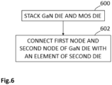
- a first step 600 (STACK GaN DIE AND MOS DIE), the first and second chips 100, 300 are superimposed for example so as to place the element 350 opposite the source pads 142, 144 as well as the surface of the electronic component 120.
- the nodes N1 and N2 are disconnected at this stage.
- a second step 602 CONNECT FIRST NODE AND SECOND NODE OF GaN DIE WITH AN ELEMENT OF SECOND DIE
- the nodes N1 and N2 of the first chip 100 are electrically connected by the element 350 of the second chip.
- the connection is either direct or via a welding or brazing and/or by means of alloys and/or by the application of heat treatment and/or pressure.
- step 600 Before step 600, nodes N1 and N2 being disconnected, it is possible to test for example the resistance of component 120 and/or a leakage current of the gate of GaN transistor 102.
- element 350 may be formed by a plurality of conductive points or surfaces.
- the second chip 300 is stacked on the first chip 100, however it is conceivable for the person skilled in the art to provide the reverse.
- the described embodiments can be applied for example for power-using applications such as for example automotive applications.
Landscapes
- Semiconductor Integrated Circuits (AREA)
- Junction Field-Effect Transistors (AREA)
- Logic Circuits (AREA)
Applications Claiming Priority (1)
| Application Number | Priority Date | Filing Date | Title |
|---|---|---|---|
| FR2310184A FR3153466A1 (fr) | 2023-09-26 | 2023-09-26 | Circuit électronique |
Publications (1)
| Publication Number | Publication Date |
|---|---|
| EP4531104A1 true EP4531104A1 (de) | 2025-04-02 |
Family
ID=90717687
Family Applications (1)
| Application Number | Title | Priority Date | Filing Date |
|---|---|---|---|
| EP24201681.4A Pending EP4531104A1 (de) | 2023-09-26 | 2024-09-20 | Elektronische schaltung |
Country Status (4)
| Country | Link |
|---|---|
| US (1) | US20250105227A1 (de) |
| EP (1) | EP4531104A1 (de) |
| CN (2) | CN223624996U (de) |
| FR (1) | FR3153466A1 (de) |
Citations (3)
| Publication number | Priority date | Publication date | Assignee | Title |
|---|---|---|---|---|
| US20140061884A1 (en) * | 2011-03-07 | 2014-03-06 | Texas Instruments Incorporated | Stacked die power converter |
| US20190035707A1 (en) * | 2017-07-14 | 2019-01-31 | Shindengen Electric Manufacturing Co., Ltd. | Electronic module |
| US20200356085A1 (en) * | 2019-05-08 | 2020-11-12 | Ares Technologies, Inc. | Apparatus and methods for testing circuit elements at one or more manufacturing stages |
-
2023
- 2023-09-26 FR FR2310184A patent/FR3153466A1/fr active Pending
-
2024
- 2024-09-19 US US18/890,617 patent/US20250105227A1/en active Pending
- 2024-09-20 EP EP24201681.4A patent/EP4531104A1/de active Pending
- 2024-09-24 CN CN202422325395.4U patent/CN223624996U/zh active Active
- 2024-09-24 CN CN202411329178.0A patent/CN119725312A/zh active Pending
Patent Citations (3)
| Publication number | Priority date | Publication date | Assignee | Title |
|---|---|---|---|---|
| US20140061884A1 (en) * | 2011-03-07 | 2014-03-06 | Texas Instruments Incorporated | Stacked die power converter |
| US20190035707A1 (en) * | 2017-07-14 | 2019-01-31 | Shindengen Electric Manufacturing Co., Ltd. | Electronic module |
| US20200356085A1 (en) * | 2019-05-08 | 2020-11-12 | Ares Technologies, Inc. | Apparatus and methods for testing circuit elements at one or more manufacturing stages |
Also Published As
| Publication number | Publication date |
|---|---|
| FR3153466A1 (fr) | 2025-03-28 |
| US20250105227A1 (en) | 2025-03-27 |
| CN119725312A (zh) | 2025-03-28 |
| CN223624996U (zh) | 2025-12-02 |
Similar Documents
| Publication | Publication Date | Title |
|---|---|---|
| US6084895A (en) | Semiconductor laser apparatus | |
| WO2018096245A1 (fr) | Circuit integre forme d'un empilement de deux puces connectees en serie | |
| FR2931586A1 (fr) | Procede de fabrication et de test d'un circuit electronique integre | |
| WO2018091852A1 (fr) | Circuit intégré forme de deux puces connectées en série | |
| EP4531104A1 (de) | Elektronische schaltung | |
| FR2849538A1 (fr) | Composant discret comprenant des diodes hf en serie et a cathode commune | |
| EP4141915A1 (de) | Verfahren zur herstellung eines verkapselten mikrochips im chipmassstab sowie die entsprechende vorrichtung | |
| FR2961345A1 (fr) | Circuit integre passif | |
| FR3097683A1 (fr) | Connexion de plusieurs circuits d'une puce électronique | |
| EP2750183A1 (de) | Integrierter Schaltkreis, und Herstellungsverfahren eines integrierten Schaltkreises, der mit einer Temperatursonde ausgestattet ist | |
| EP3477698B1 (de) | Integrierter schaltkreis in einem qfn-gehäuse | |
| FR2894070A1 (fr) | Module electronique 3d | |
| WO2017203185A1 (fr) | Dispositif a haute mobilite electronique avec elements passifs integres | |
| EP4651204A1 (de) | Verfahren zur herstellung von elektronischen bauteilen mit benetzbaren flanken | |
| FR3156587A1 (fr) | Procédé de fabrication de composants électroniques | |
| FR2962578A1 (fr) | Composant électronique en boitier céramique | |
| FR3158588A1 (fr) | Procédé de fabrication de composants électroniques | |
| FR3155948A1 (fr) | Procédé de fabrication de composants électroniques à flancs mouillables | |
| FR3090264A1 (fr) | Procédé de montage de composant | |
| FR3153185A1 (fr) | Composant électronique | |
| WO2003038746A1 (fr) | Languette deformable integree a un module pour raccordement electrique a coeur | |
| EP1350418A1 (de) | Verfahren zur herstellung einer verbindung in mehrschichtigen leiterplatten | |
| FR3167037A1 (fr) | Procédé de fabrication d’interconnexion pour un dispositif électronique | |
| FR3145834A1 (fr) | Composant de liaison de signaux de boîtier de semi-conducteur de puissance et module à semi-conducteur | |
| FR3125357A1 (fr) | Procédé de fabrication de puces électroniques |
Legal Events
| Date | Code | Title | Description |
|---|---|---|---|
| PUAI | Public reference made under article 153(3) epc to a published international application that has entered the european phase |
Free format text: ORIGINAL CODE: 0009012 |
|
| STAA | Information on the status of an ep patent application or granted ep patent |
Free format text: STATUS: REQUEST FOR EXAMINATION WAS MADE |
|
| 17P | Request for examination filed |
Effective date: 20240920 |
|
| AK | Designated contracting states |
Kind code of ref document: A1 Designated state(s): AL AT BE BG CH CY CZ DE DK EE ES FI FR GB GR HR HU IE IS IT LI LT LU LV MC ME MK MT NL NO PL PT RO RS SE SI SK SM TR |