EP4531280A1 - Module frontal multigénérationnel (fem) - Google Patents
Module frontal multigénérationnel (fem) Download PDFInfo
- Publication number
- EP4531280A1 EP4531280A1 EP24203336.3A EP24203336A EP4531280A1 EP 4531280 A1 EP4531280 A1 EP 4531280A1 EP 24203336 A EP24203336 A EP 24203336A EP 4531280 A1 EP4531280 A1 EP 4531280A1
- Authority
- EP
- European Patent Office
- Prior art keywords
- fem
- power amplifier
- amplifier
- circuit
- mode
- Prior art date
- Legal status (The legal status is an assumption and is not a legal conclusion. Google has not performed a legal analysis and makes no representation as to the accuracy of the status listed.)
- Pending
Links
Images










Classifications
-
- H—ELECTRICITY
- H03—ELECTRONIC CIRCUITRY
- H03F—AMPLIFIERS
- H03F3/00—Amplifiers with only discharge tubes or only semiconductor devices as amplifying elements
- H03F3/20—Power amplifiers, e.g. Class B amplifiers, Class C amplifiers
- H03F3/24—Power amplifiers, e.g. Class B amplifiers, Class C amplifiers of transmitter output stages
- H03F3/245—Power amplifiers, e.g. Class B amplifiers, Class C amplifiers of transmitter output stages with semiconductor devices only
-
- H—ELECTRICITY
- H03—ELECTRONIC CIRCUITRY
- H03F—AMPLIFIERS
- H03F1/00—Details of amplifiers with only discharge tubes, only semiconductor devices or only unspecified devices as amplifying elements
- H03F1/02—Modifications of amplifiers to raise the efficiency, e.g. gliding Class A stages, use of an auxiliary oscillation
- H03F1/0205—Modifications of amplifiers to raise the efficiency, e.g. gliding Class A stages, use of an auxiliary oscillation in transistor amplifiers
- H03F1/0211—Modifications of amplifiers to raise the efficiency, e.g. gliding Class A stages, use of an auxiliary oscillation in transistor amplifiers with control of the supply voltage or current
-
- H—ELECTRICITY
- H03—ELECTRONIC CIRCUITRY
- H03F—AMPLIFIERS
- H03F1/00—Details of amplifiers with only discharge tubes, only semiconductor devices or only unspecified devices as amplifying elements
- H03F1/02—Modifications of amplifiers to raise the efficiency, e.g. gliding Class A stages, use of an auxiliary oscillation
- H03F1/0205—Modifications of amplifiers to raise the efficiency, e.g. gliding Class A stages, use of an auxiliary oscillation in transistor amplifiers
- H03F1/0261—Modifications of amplifiers to raise the efficiency, e.g. gliding Class A stages, use of an auxiliary oscillation in transistor amplifiers with control of the polarisation voltage or current, e.g. gliding Class A
-
- H—ELECTRICITY
- H03—ELECTRONIC CIRCUITRY
- H03F—AMPLIFIERS
- H03F1/00—Details of amplifiers with only discharge tubes, only semiconductor devices or only unspecified devices as amplifying elements
- H03F1/56—Modifications of input or output impedances, not otherwise provided for
-
- H—ELECTRICITY
- H03—ELECTRONIC CIRCUITRY
- H03F—AMPLIFIERS
- H03F3/00—Amplifiers with only discharge tubes or only semiconductor devices as amplifying elements
- H03F3/189—High-frequency amplifiers, e.g. radio frequency amplifiers
- H03F3/19—High-frequency amplifiers, e.g. radio frequency amplifiers with semiconductor devices only
- H03F3/195—High-frequency amplifiers, e.g. radio frequency amplifiers with semiconductor devices only in integrated circuits
-
- H—ELECTRICITY
- H03—ELECTRONIC CIRCUITRY
- H03F—AMPLIFIERS
- H03F3/00—Amplifiers with only discharge tubes or only semiconductor devices as amplifying elements
- H03F3/68—Combinations of amplifiers, e.g. multi-channel amplifiers for stereophonics
-
- H—ELECTRICITY
- H03—ELECTRONIC CIRCUITRY
- H03F—AMPLIFIERS
- H03F3/00—Amplifiers with only discharge tubes or only semiconductor devices as amplifying elements
- H03F3/72—Gated amplifiers, i.e. amplifiers which are rendered operative or inoperative by means of a control signal
-
- H—ELECTRICITY
- H04—ELECTRIC COMMUNICATION TECHNIQUE
- H04B—TRANSMISSION
- H04B1/00—Details of transmission systems, not covered by a single one of groups H04B3/00 - H04B13/00; Details of transmission systems not characterised by the medium used for transmission
- H04B1/38—Transceivers, i.e. devices in which transmitter and receiver form a structural unit and in which at least one part is used for functions of transmitting and receiving
- H04B1/40—Circuits
- H04B1/401—Circuits for selecting or indicating operating mode
-
- H—ELECTRICITY
- H03—ELECTRONIC CIRCUITRY
- H03F—AMPLIFIERS
- H03F2200/00—Indexing scheme relating to amplifiers
- H03F2200/111—Indexing scheme relating to amplifiers the amplifier being a dual or triple band amplifier, e.g. 900 and 1800 MHz, e.g. switched or not switched, simultaneously or not
-
- H—ELECTRICITY
- H03—ELECTRONIC CIRCUITRY
- H03F—AMPLIFIERS
- H03F2200/00—Indexing scheme relating to amplifiers
- H03F2200/387—A circuit being added at the output of an amplifier to adapt the output impedance of the amplifier
-
- H—ELECTRICITY
- H03—ELECTRONIC CIRCUITRY
- H03F—AMPLIFIERS
- H03F2200/00—Indexing scheme relating to amplifiers
- H03F2200/451—Indexing scheme relating to amplifiers the amplifier being a radio frequency amplifier
-
- H—ELECTRICITY
- H03—ELECTRONIC CIRCUITRY
- H03F—AMPLIFIERS
- H03F2203/00—Indexing scheme relating to amplifiers with only discharge tubes or only semiconductor devices as amplifying elements covered by H03F3/00
- H03F2203/72—Indexing scheme relating to gated amplifiers, i.e. amplifiers which are rendered operative or inoperative by means of a control signal
- H03F2203/7209—Indexing scheme relating to gated amplifiers, i.e. amplifiers which are rendered operative or inoperative by means of a control signal the gated amplifier being switched from a first band to a second band
Definitions
- the technology of the disclosure relates generally to a technique to provide a front-end module (FEM) that will work with multiple generations of wireless standards.
- FEM front-end module
- newer wireless protocols While the newer wireless protocols have more bandwidth than the older wireless protocols, the infrastructure deployed to support the older wireless protocols remains deployed in some locales. Further, newer protocols may do some form of aggregation that utilizes signaling in multiple protocols simultaneously to increase bandwidth. Accordingly, many wireless communication devices may include circuitry that supports a plurality of wireless protocols. Providing a cost-effective solution that fits within the space available in commercially viable wireless communication devices provides an opportunity for innovation.
- a FEM having a single transmission path may include a single power amplifier with supporting elements such as, for example, bias levels, load modulation, supply voltages, or the like, that may be reconfigured and tuned so as to allow the single power amplifier to adapt effectively and work with different generations of wireless protocols.
- the use of such an adaptive, reconfigurable, tunable transmission path allows smaller and more cost-effective FEMs to be provided.
- Settings for the various changes may be stored in a look-up table (LUT) or the like.
- tuning and adjustments used to switch between generations may be implemented in a silicon stage that is positioned before a primary amplifier stage that is formed in a different material (e.g., gallium arsenide (GaAs)) along with a second silicon stage that is positioned after the primary amplifier stage.
- a silicon stage that is positioned before a primary amplifier stage that is formed in a different material (e.g., gallium arsenide (GaAs)) along with a second silicon stage that is positioned after the primary amplifier stage.
- GaAs gallium arsenide
- a FEM in one aspect, includes a main power amplifier, a plurality of adjustable elements associated with the main power amplifier, and a control circuit coupled to each of the plurality of adjustable elements.
- the control center is configured to, in response to receiving a command to operate the main power amplifier in a second-generation cellular mode, command at least one of the plurality of adjustable elements to change operation based on information in a look-up table, and in response to receiving a second command to operate the main power amplifier in a subsequent generation cellular mode, command the at least one of the plurality of adjustable elements to change operation.
- a mobile communication device in another aspect, includes a baseband processor (BBP), a transceiver circuit coupled to the BBP, an antenna, and a FEM coupled to the antenna and the transceiver circuit.
- the FEM includes a main power amplifier, a plurality of adjustable elements associated with the main power amplifier, and a control circuit coupled to each of the plurality of adjustable elements.
- the control circuit is configured to, in response to receiving a command to operate the main power amplifier in a second-generation cellular mode, command at least one of the plurality of adjustable elements to change operation based on information in a look-up table, and in response to receiving a second command to operate the main power amplifier in a subsequent generation cellular mode, command the at least one of the plurality of adjustable elements to change operation.
- a method of changing operation of a FEM includes receiving an indication at the FEM for operation in a second-generation cellular mode. The method also includes, responsive to receiving the indication, causing at least one adjustable element in the FEM to change operation, receiving a second indication at the FEM for operation in a subsequent generation cellular mode, and responsive to receiving the second indication, causing the at least one adjustable element in the FEM to change operation.
- a FEM in another aspect, includes a primary power amplifier stage and a silicon prestage structure positioned in front of the primary power amplifier stage, the silicon prestage structure comprising a plurality of adjustable elements associated with the primary power amplifier stage.
- the FEM also includes a control circuit coupled to each of the plurality of adjustable elements and configured to responsive to receiving a command to operate the primary power amplifier stage in a first mode, command at least one of the plurality of adjustable elements to change operation based on information in a LUT and responsive to receiving a second command to operate the primary power amplifier stage in a different mode, command the at least one of the plurality of adjustable elements to change operation.
- transceiver In keeping with the above admonition about definitions, the present disclosure defines "transceiver.”
- Current industry literature uses the term “transceiver” in two primary ways. In a first meaning, the term refers broadly to a plurality of circuits that send and receive signals. In this broader context, example circuits may include a baseband processor, an up/down conversion circuit, filters, amplifiers, couplers, and the like coupled to one or more antennas.
- some authors in the industry literature refer specifically to a circuit positioned between a baseband processor and a power amplifier circuit as a transceiver. This intermediate circuit may include the up/down conversion circuits, mixers, oscillators, filters, and the like, but generally does not include the power amplifiers.
- transceiver is used in the first sense. Where relevant to distinguish between the two definitions, the terms “transceiver chain” and “transceiver circuit” are used respectively.
- ENDC is a multilayer acronym with multiple layers of embedded acronyms whose explication interrupts the flow of normal prose. Rather than try to work the explanation into normal prose, the expansion of this acronym is set forth here for simplicity. Specifically, ENDC stands for E-UTRAN New Radio - Dual Connectivity, where E-UTRAN stands for Evolved Universal Terrestrial Radio Access Network or sometimes Evolved UMTS Terrestrial Radio Access Network, where UMTS stands for Universal Mobile Telecommunications Service.
- a FEM having a single transmission path may include a single power amplifier with supporting elements such as for example, bias levels, load modulation, supply voltages, or the like, that may be reconfigured and tuned so as to allow the single power amplifier to adjust effectively and work with different generations of wireless protocols.
- the use of such an adjustable, reconfigurable, tunable transmission path allows smaller and more cost-effective FEM to be provided. Settings for the various changes may be stored in a look-up table (LUT) or the like.
- tuning and adjustments used to switch between generations may be implemented in a silicon stage that is positioned before a primary amplifier stage that is formed in a different material (e.g., gallium arsenide (GaAs)) along with a second silicon stage that is positioned after the primary amplifier stage.
- a silicon stage that is positioned before a primary amplifier stage that is formed in a different material (e.g., gallium arsenide (GaAs)) along with a second silicon stage that is positioned after the primary amplifier stage.
- GaAs gallium arsenide
- FIG. 1A Before addressing example aspects of the present disclosure, a discussion of parts of a transmission path in a transceiver is provided with reference to Figure 1A .
- a discussion of a device having a plurality of transmission paths follows with respect to Figures 1B and 1C .
- Figures 2A and 2B illustrate various possible FEMs that are designed to accommodate the plurality of transmission paths to help illustrate some of the challenges of conventional mobile communication devices. Aspects of the present disclosure consolidate transmission paths in a FEM, and the discussion of these aspects begins below with reference to Figure 3A .
- FIG. 1A illustrates a first transmission path 100 that may begin in an application processor (AP) 102.
- Data generated in the AP 102 is passed to a baseband processor (BBP) 104 and formatted into a signal for transmission.
- the signal for transmission may optionally be upconverted and conditioned by a transceiver circuit 106.
- the signal then goes to a FEM 108 and then is radiated out through an antenna 110.
- a mobile computing device 120 may include the first transmission path 100 as well as a BLUETOOTH transmission path 122 and a WIFI transmission path 124.
- the BLUETOOTH transmission path 122 is coupled to the AP 102 and includes a BBP 126, an optional transceiver circuit 128, a FEM 130, and an antenna 132.
- the BLUETOOTH transmission path 122 is configured to prepare and send signals complying with the BLUETOOTH protocol.
- the WIFI transmission path 124 is coupled to the AP 102 and includes a BBP 134, an optional transceiver circuit 136, a FEM 138, and an antenna 140.
- the WIFI transmission path 124 is configured to prepare and send signals complying with the WIF protocol. While not shown, there may be transmission paths for other wireless protocols in the mobile computing device 120.
- antennas may be shared across transmission paths.
- a shared antenna 150 may be provided for the mobile computing device 120'.
- a multiplexer or switch 152 may route signals from transmission paths 100', 122', and 124' to the antenna 150.
- Figure 2A illustrates a conventional FEM 108A (that may take the place of FEM 108 in a conventional mobile computing device) that may include a 2G module 200, a linear late generation module 202, and an optional ENDC module 204.
- the 2G module 200 may include a first low bandwidth power amplifier 206 with a first low bandwidth output match circuit 208, a second medium bandwidth power amplifier 210, and a second medium bandwidth output match circuit 212.
- the 2G module 200 may serve to amplify and condition signals complying with 2G cellular protocols. It should be appreciated that 2G protocols may operate both in a linear mode (Lin) as well as a Vramp mode.
- the linear late generation module 202 may include a third power amplifier 214 and a third output match circuit 216.
- the second medium bandwidth power amplifier 210 and the third power amplifier 214 are duplicative.
- the second medium bandwidth output match circuit 212 and the third output match circuit 216 are duplicative.
- the linear late generation module 202 may serve to amplify and condition signals complying with 3G, 4G, and/or 5G cellular protocols.
- the ENDC module 204 may include a fourth power amplifier 218, a fourth output match circuit 220, and a filter 222.
- the fourth power amplifier is duplicative relative to the second medium bandwidth power amplifier 210 and the third power amplifier 214.
- the fourth output match circuit 220 is duplicative relative to the second medium bandwidth output match circuit 212 and the third output match circuit 216.
- the ENDC module 204 may be used to provide a second signal path in a desired protocol (usually 4G) that is used for carrier aggregation.
- the various modules 200, 202, and 204 are coupled to the antenna 110A (and optionally antenna 110B) through a multiplexer or switch 224.
- the antenna 110B may be provided to assist in carrier aggregation or diversity transmission as is well understood.
- the antennas 110A, 110B may be antenna arrays able to do beam steering, as is well understood.
- the switch 224 may be within one of the modules.
- the modules 200, 202, and 204 may be encapsulated in a unitary mold compound so that the FEM 108A may be sold as a single unit. Alternatively, and not shown, the module 204 may be in a separate device (e.g., on a different substrate outside the encapsulation of the modules 200 and 202).
- the FEM 108B may include the ENDC module 204, as previously described, as well as a combined module 230.
- the combined module 230 includes a first low bandwidth power amplifier 206 with a first low bandwidth output match circuit 208 and a second medium bandwidth power amplifier 210, and a second medium bandwidth output match circuit 212.
- the combined module 230 also includes a third power amplifier 214 and a third output match circuit 216.
- An antenna switch 232 may couple the different paths to the antennas 110A, 110B.
- a switch 234 may couple the output match circuit 216 to different filters 236(1)-236(3).
- the filters 236(1)-236(3) may be optimized for a given one of the later linear generations (i.e., 3G-5G).
- the power amplifiers are duplicative as are the output match circuits.
- duplication of the power amplifiers and the output match circuits increases the overall cost of the FEM as well as makes the FEM larger. Both increased cost and increased size are commercially undesirable. Further, having duplicative circuits may increase leakage current, which may incrementally increase power consumption. Likewise, having multiple paths means more conductors coming into the FEM with appurtenant routing issues, which may further exacerbate the size issues.
- Example aspects of the present disclosure consolidate at least the linear portion of the 2G path with the later linear generation paths. Because of the different bandwidths, power requirements, class of operation, and the like, such consolidation requires flexibility in other elements of the FEM.
- the following Figures explore some of the various ways to make the FEM adaptable, tunable, and reconfigurable.
- Figure 3A illustrates a first FEM 300A, where the linear 2G path is consolidated into the linear later generation path, that is, into a multigenerational main power amplifier 302.
- An ENDC path with an ENDC power amplifier 304 and a 2G medium bandwidth path with a 2G amplifier 306 (sometimes also referred to as Vramp) remain distinct paths with their own power amplifiers and supporting circuitry.
- Figure 3B illustrates a second FEM 300B where the linear 2G path is consolidated into the ENDC path to form a multigenerational power amplifier 310.
- the linear later generation path with basic multigenerational power amplifier 312 (perhaps limited to just 3G-5G) and the 2G medium bandwidth path with the 2G amplifier 306 remain distinct paths with their own power amplifiers and supporting circuitry. Elimination of the low bandwidth path and consolidation of power amplifier elements and output match circuit elements reduces the overall size of the FEM as well as reduces the cost of the FEM. Note that optionally the 2G Vramp may also be integrated into the consolidated path. While other elements of the FEM will be made tunable or reconfigurable to adapt to the operating mode, the overall effect retains cost savings and space reduction. The following Figures explore the details of the changes to the other elements.
- any given amplifier may seemingly be described as a single amplifier, any given amplifier may be formed from multiple stages or multiple stacked transistors (e.g., cascoded). Likewise, it should be appreciated that the amplifiers may be bipolar junction transistors (BJT) or field effect transistors (FETs).
- BJT bipolar junction transistors
- FETs field effect transistors
- Figure 4 illustrates a FEM 400 (which may be either FEM 300A or 300B) that highlights the changes to the supporting elements to make the power amplifier 402 able to provide desired amplification to a signal in any of the 2G-5G (and subsequent generations) cellular standards. It should be appreciated that the different modes of operation need rather different maximum power levels, gain, and class of operation, as well as a requirement for predictable operation in different frequency bands and differently sized signal bandwidths.
- CMOS complementary metal oxide semiconductor
- GaAs gallium arsenide
- driver amplifier 404 may make for easier implementation because reconfiguration of certain types is generally easier in CMOS structures. It should be noted that other types of reconfigurations may be better done in silicon, as better explained beginning below with reference to Figure 15A .
- a PMIC 408 provides a supply voltage to the power amplifier 402.
- the PMIC 408 may be a buck-boost DC-DC converter that changes between a boost mode for 2G and high power 3G-5G modes and a buck mode for most low and mid-power modes.
- a more in-depth discussion of the PMIC 408 is provided below in Figures 5-6B .
- the different modes may need different classes of operation (e.g., A, AB, B, C, F, inverted F, etc.) of the power amplifier 402.
- 3G-5G may use class AB for the power amplifier 402 and the driver amplifier 404, while the 2G Vramp may use class C operation.
- An impedance adaptation circuit 410 may be provided to compensate for impedance variation of the active stage.
- a harmonic trap circuit 412 may be used at an output of the power amplifier 402 to assist in adapting to the different classes of operation.
- Another adaptation is the use of an adaptable load line tuning circuit 414. It should be appreciated that since this occurs at the output of the power amplifier 402, switching the load line impedance involves some efficiency loss. This efficiency loss makes wide-range load impedance tuning less attractive, but it remains an option to assist in providing the multigenerational power amplifier of the present disclosure.
- Matching circuits 416(1) and 416(2) may provide impedance matching or the like and may if desired, be configurable to assist in conditioning a signal for amplification or the like.
- Adjustable bias circuits 418(1) and 418(2) may control the bias for the power amplifier 402 and the driver amplifier 404, respectively. By making these bias values adjustable, the operation of the amplifiers may be tailored to the desired mode.
- an input signal may be demultiplexed (DeMUX) by a demultiplexer 420.
- 2G signals may pass through a match circuit 422 and then to the predriver amplifier 406.
- An adjustable bias circuit 424 may bias the predriver amplifier 406. The adaption of the adjustable bias circuit 424 may be somewhat constrained because the predriver amplifier 406 is only switching between 2G Vramp and linear 2G.
- 3G-5G signals pass through the demultiplexer 420 and may be variably attenuated by variable attenuator 426.
- the 2G-5G paths are recombined by a multiplexer (MUX) 428 before going to the matching circuit 416(1) and the main consolidated transmission path.
- MUX multiplexer
- Knowing what mode is active so that the adjustments can be made may come from information provided by the BBP (not shown in Figure 4 ) through a bus interface 430 (also referred to as a digital input/output (I/O)) and an associated control circuit (not shown).
- a bus interface 430 also referred to as a digital input/output (I/O)
- I/O digital input/output
- Figure 4 shows some of the possible tuning and adaptations that may be made to accommodate the multigenerational demands, the details are numerous.
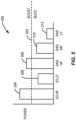
- Figure 5 illustrates a bar graph 500, which shows the various modes and their power requirements.
- Line 502 shows an abstract representation of where the DC-DC converter switches between buck to boost modes.
- the 2G high power column 504 and high-power later generation column 506 are boost modes and the remaining columns (i.e., 2G low power column 508, later generation midpower column 510 and later generation low power column 512) are all buck mode power requirements.
- the present disclosure contemplates a special PMIC 408, as better illustrated in Figures 6A and 6B .
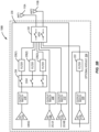
- the PMIC 408 has a first buck-boost DC-DC converter 600 and a second buck-boost DC-DC converter 602, along with a control circuit 604.
- the control circuit 604 controls how and when the outputs of the DC-DC converters 600 and 602 are combined.
- switches 606(1)-606(4) may be controlled by the control circuit 604 to direct a combined power signal to a multigenerational power amplifier 310, or a single switch 606(1) may provide a single power signal to the basic multigenerational power amplifier 312 as shown in Figure 6A .
- switches 608(1)-608(4) may provide a combined power signal to the multigenerational main power amplifier 302, and a single switch 608(1) may provide a single power signal to the ENDC power amplifier 304.
- a local control circuit in the FEM may provide instructions to each element by writing appropriate values into a corresponding setting register (not shown) after retrieving such values from a local memory (e.g., a LUT). While, in theory, the local control circuit could calculate these values dynamically, current commercial constraints on the size and power of the control circuit preclude such an approach, and a local LUT is more practical.
- the BBP 104 could send values over the communication bus to the FEM. These values could be stored in memory (e.g., in a LUT) in the BBP 104 or calculated dynamically.
- the current communication bus under the current MIPI standard is a fairly narrow band channel, and the volume of settings would likely exceed the bandwidth capacity of the bus under the current MIPI standard.
- example aspects of the present disclosure contemplate a local control circuit 700 using a local memory 702 (which may be read-only memory (ROM)) to store settings for per mode optimization.
- these settings are stored in a LUT.
- LUT may be a multipage LUT and store information such as settings for an input match circuit, an interstage match circuit, an output match circuit, a harmonic filter, attenuation settings, reconfiguration, class settings, linearization, analog predistortion, and the like.
- some settings may still come from the BBP 104, such as the band, mode, power level, bias settings, or the like.
- some of the adjustable elements may be formed in CMOS structures and may be controlled through a corresponding digital to analog (DAC) 704(1)-704(N).
- DAC digital to analog
- Figure 8 illustrates a graph 800 showing how capacitance on y-axis 802 varies as a function of input voltage on x-axis 804. While class A and class C operations are fairly stable, class AB has a large capacitance variation.
- aspects of the present disclosure may include a tunable capacitive element at an input to a power amplifier as better seen in Figures 9A and 9B .
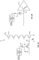
- a CMOS power amplifier 900 formed from a stack of cascoded FETs 902(1)-902(M)
- an input 904 may receive a bias signal from an adjustable bias circuit 418 as well as have this bias signal pass through a tunable capacitance circuit 906 and a variable resistor 908.
- the tunable capacitance circuit 906 may be programmed by DAC (not shown) to sum with the input capacitance of the power amplifier 900 to provide a constant total input capacitance.
- a tunable capacitance circuit 922 may be provided between the adjustable bias circuit 418 and the input 924 of the power amplifier 920. Still, other arrangements are possible without departing from the present disclosure.
- FIG. 10 illustrates a FEM 1000 having a predriver amplifier 1002, a driver amplifier 1004, and a main power amplifier 1006.
- a control circuit 1008 may provide settings for setting registers (not shown explicitly) for a first bias circuit 1010 that biases the predriver amplifier 1002, a second bias circuit 1012 that biases the driver amplifier 1004, and a third bias circuit 1014 that biases the main power amplifier 1006.
- the control circuit 1008 may adapt a bandwidth for each amplifier 1002, 1004, 1006 using bandwidth adjustment circuits 1016, 1018, and 1020 respectively.
- the control circuit 1008 may adapt frequency per band using DACs 1022, 1024, and 1026 for amplifiers 1002, 1004, and 1006 respectively.
- the 2G Vramp is also included in the multigenerational power amplifier, it may be appropriate to provide a closed loop bias, as better seen in Figure 11 , where a FEM 1100 has power amplifiers 1002, 1004, and 1006 along with bias circuits 1010, 1012, and 1014, as previously described as well as other components described above, but not replicated for simplicity.
- a power detector 1102 may be present at an output of the power amplifier 1006 and provide a feedback signal to a Vramp amplifier 1104 and power control circuit 1106.
- the signals from the power control circuit 1106 may be combined with the bias signals for each of the power amplifiers 1002, 1004, and 1006. Note that the signals need not be uniform.
- FIG 12 illustrates an analog-pre-distribution (APD) circuit 1200 used with the FEM 1100.
- a power detector 1202 senses power in the driver amplifier 1004 and may provide a signal to the adaptive bias circuit 1012.
- Figure 12 also provides additional details about a possible circuit for the bias circuit 1012.
- the bias circuit 1012 may be a form of open loop bias and is given by a diode connected FET 1204 in mirror 1206. If no current is injected into the kick resistor 1208, the bias voltage (Vbias) is equal to the Vgs of the diode connected FET 1204.
- the kick resistor 1208 may also be used to help linearize the amplitude modulation-amplitude modulation (AM-AM) APD by the APD circuit 1200.
- AM-AM amplitude modulation-amplitude modulation
- Variable capacitors e.g., capacitor DACs
- 1210(1)-1210(3) may be used to adapt the bandwidth of the bias and reduce the noise impact of the kick resistor 1208.
- bias circuit 1300 eliminates the kick resistor, thereby reducing the noise and reducing the need for bias bandwidth adjustment.
- APD and Vramp power control are done with fast mirrors 1302, 1304 in place of the kick resistor.
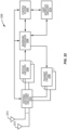
- a BBP sends information to the FEM where the information contains a mode and band (and optionally bias and/or power levels) (block 1402).
- the control circuit in the FEM determines what settings are needed based on the mode and band information from the BBP (block 1404).
- the control circuit pulls settings from the LUT (block 1406) and writes the settings to the settings registers for the adjustable elements within the FEM (block 1408).
- the adjustable elements do adjust based on the new settings in the settings registers (block 1410), and the signal is amplified using the new configuration (block 1412).
- a primary amplifier chip may have a prestage structure that precedes an input to the driver amplifier of the primary amplifier chip and a poststage structure that follows an output of the output stage amplifier.
- the prestage and poststage structures may be implemented in silicon and may be part of the same physical device (e.g., same chip or module).
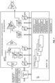
- Figures 15A & 15B illustrate an amplifier chain 1500 with a transceiver circuit 1502, a prestage structure 1504, a primary amplifier structure 1506, and a poststage structure 1508.
- the primary amplifier structure 1506 is made from GaAs or the like and includes a driver amplifier (e.g., driver amplifier 404) and an output stage amplifier (e.g., the output stage amplifier - i.e., power amplifier 402).
- the prestage structure 1504 and the poststage structure 1508 are made from silicon.
- the prestage structure 1504 may include a predriver amplifier (e.g., predriver amplifier 406) and supporting circuitry.
- the poststage structure 1508 may include switching networks, impedance matching circuits, filters, and the like (e.g., load line tuning circuits 414 and harmonic trap circuits 412). Additionally, a control circuit 1510 may also be implemented in silicon. The control circuit 1510 may also be co-located with bias circuitry (not shown) that works with the primary amplifier structure 1506. In one aspect, the structures 1504, 1508, and the control circuit 1510 are in the same chip, but such an arrangement is not required.
- the DC-DC converter 1512A is a buck-boost converter that has the ability to boost the signal to the high levels required by 2G systems (e.g., the dual PMIC 408) and may directly connect to the primary amplifier structure 1506.
- the DC-DC converter 1512B has a bypass switch 1514 that allows Vbatt to couple directly to the primary amplifier structure 1506 so as to provide the high power required for 2G operation.
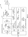
- Figure 16 provides some additional details about possible ways to implement the prestage structure 1504 in which elements already discussed may be positioned in the silicon of the prestage structure 1504.
- signals arrive and are demultiplexed by demultiplexer 420.
- 2G signals may go through the predriver amplifier 406, while other signals may go through the variable attenuator 426.
- the signals are multiplexed by the mux 428.
- the variable CDACs 704(1) are used to control variations between modes at this stage.
- the local memory 702 and registers 1600 may be used to control the variable attenuator 426 and CDACs 704(1).
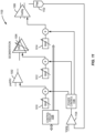
- Figure 17 expands on the prestage structure 1504 showing how a power detector 1700 may detect power at the input to provide information to an input power limiter circuit 1702.
- the input power limiter circuit 1702 may use information about the input power to set DACs 1704(1)-1704(3) that assist in controlling the bias circuits 424, 418(1), and 418(2).
- This arrangement may assist in protecting the circuits from overpower conditions based on mode. That is, certain modes may need different power levels, as previously described, and the ability to control the biases to stay within the desired power level of the mode is desirable.
- the input signal may vary in different ranges depending on the mode, and adapting to that input is desirable.
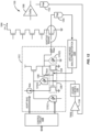
- Figure 18 adds an output power detector 1800 in the poststage structure 1508, which may be used by a power protection circuit 1802 to adjust bias circuits 418(1), 418(2).
- the various modes may require different power levels, and while the various adjustments made possible by the present disclosure contemplate dialing in the power levels to the desired levels through the adjustments, having an additional protection circuit may assist in preventing damage from overpower conditions.
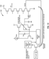
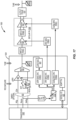
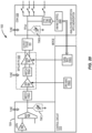
- Figure 19 illustrates another option in terms of a protection circuit. More particularly, a voltage detector 1900 may snoop the supply voltages supplied to the driver amplifier 404 and/or the power amplifier 402. A current detector 1902 may detect a bias current provided to the power amplifier 402. This information may then be provided to an overcurrent protection circuit 1904, which with information from the power detector 1700 and the output power detector 1800, may determine when an overcurrent condition exists and adjust one or more bias circuits, such as the output bias circuit 418(1).
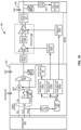
- Figure 21 adds an AM-PM APD circuit 2100 that receives information about a phase distortion and uses a variable capacitor 2102 to inject phase predistortion either at the interstage matching circuit 416(1) or the interstage matching circuit 416(2).
- the user elements 2200 may be implemented in various types of user elements 2200, such as mobile terminals, smart watches, tablets, computers, navigation devices, access points, and like wireless communication devices that support wireless communications, such as cellular, wireless local area network (WLAN), Bluetooth, and near field communications.
- the user elements 2200 will generally include a control system 2202, a baseband processor 2204, transmit circuitry 2206, receive circuitry 2208, antenna switching circuitry 2210, multiple antennas 2212, and user interface circuitry 2214.
- the control system 2202 can be a field-programmable gate array (FPGA) or an application-specific integrated circuit (ASIC), as an example.
- FPGA field-programmable gate array
- ASIC application-specific integrated circuit
- control system 2202 can include at least a microprocessor(s), an embedded memory circuit(s), and a communication bus interface(s).
- the receive circuitry 2208 receives radio frequency signals via the antennas 2212 and through the antenna switching circuitry 2210 from one or more base stations.
- a low noise amplifier and a filter of the receive circuitry 2208 cooperate to amplify and remove broadband interference from the received signal for processing.
- Downconversion and digitization circuitry (not shown) will then downconvert the filtered, received signal to an intermediate or baseband frequency signal, which is then digitized into one or more digital streams using an analog-to-digital converter(s) (ADC).
- ADC analog-to-digital converter
- the baseband processor 2204 processes the digitized received signal to extract the information or data bits conveyed in the received signal. This processing typically comprises demodulation, decoding, and error correction operations.
- the baseband processor 2204 is generally implemented in one or more digital signal processors (DSPs) and ASICs.
- the baseband processor 2204 receives digitized data, which may represent voice, data, or control information, from the control system 2202, which it encodes for transmission.
- the encoded data is output to the transmit circuitry 2206, where a digital-to-analog converter(s) (DAC) converts the digitally encoded data into an analog signal, and a modulator modulates the analog signal onto a carrier signal that is at a desired transmit frequency or frequencies.
- DAC digital-to-analog converter
- a power amplifier will amplify the modulated carrier signal to a level appropriate for transmission and deliver the modulated carrier signal to the antennas 2212 through the antenna switching circuitry 2210 to the antennas 2212.
- the multiple antennas 2212 and the replicated transmit and receive circuitries 2206, 2208 may provide spatial diversity. Modulation and processing details will be understood by those skilled in the art.
- Clause 8 The FEM of any of clauses 1 to 7, wherein the control circuit is configured to cause the at least one of the plurality of adjustable elements to adjust an operating bandwidth.
- Clause 17 The method of clause 14, 15 or 16, further comprising combining signals from a first power amplifier whose operation is changed by the at least one adjustable element and a second power amplifier to provide carrier aggregation.
Landscapes
- Engineering & Computer Science (AREA)
- Power Engineering (AREA)
- Computer Networks & Wireless Communication (AREA)
- Signal Processing (AREA)
- Microelectronics & Electronic Packaging (AREA)
- Amplifiers (AREA)
Applications Claiming Priority (4)
| Application Number | Priority Date | Filing Date | Title |
|---|---|---|---|
| US202363586807P | 2023-09-29 | 2023-09-29 | |
| US202363542946P | 2023-10-06 | 2023-10-06 | |
| US202363607710P | 2023-12-08 | 2023-12-08 | |
| US18/891,610 US20250112601A1 (en) | 2023-09-29 | 2024-09-20 | Multigenerational front-end module (fem) |
Publications (1)
| Publication Number | Publication Date |
|---|---|
| EP4531280A1 true EP4531280A1 (fr) | 2025-04-02 |
Family
ID=92925879
Family Applications (1)
| Application Number | Title | Priority Date | Filing Date |
|---|---|---|---|
| EP24203336.3A Pending EP4531280A1 (fr) | 2023-09-29 | 2024-09-27 | Module frontal multigénérationnel (fem) |
Country Status (3)
| Country | Link |
|---|---|
| US (1) | US20250112601A1 (fr) |
| EP (1) | EP4531280A1 (fr) |
| CN (1) | CN119743160A (fr) |
Citations (10)
| Publication number | Priority date | Publication date | Assignee | Title |
|---|---|---|---|---|
| US20130027129A1 (en) * | 2011-07-27 | 2013-01-31 | Intel Mobile Communications GmbH | Transmit circuit, method for adjusting a bias of a power amplifier and method for adapting the provision of a bias information |
| US8599726B2 (en) * | 2010-06-03 | 2013-12-03 | Broadcom Corporation | Front end module with a tunable balancing network |
| EP2582038B1 (fr) * | 2011-10-14 | 2014-12-17 | BlackBerry Limited | Procédés et appareil pour contrôler la puissance |
| US20150148095A1 (en) * | 2013-11-26 | 2015-05-28 | Skyworks Solutions, Inc | Multi-mode power amplifier |
| US20180226927A1 (en) * | 2015-12-30 | 2018-08-09 | Skyworks Solutions, Inc. | Multi-mode power amplifier module |
| US10069479B1 (en) * | 2013-12-31 | 2018-09-04 | Ethertronics, Inc. | Tunable filter for RF circuits |
| EP3993261A1 (fr) * | 2020-11-02 | 2022-05-04 | Nokia Solutions and Networks Oy | Appareil radio |
| WO2023141443A1 (fr) * | 2022-01-18 | 2023-07-27 | Qorvo Us, Inc. | Fonctionnement frontal linéarisé utilisant des informations provenant d'un circuit en bande de base |
| WO2023150587A1 (fr) * | 2022-02-04 | 2023-08-10 | Qorvo Us, Inc. | Circuit de polarisation pour amplificateur de puissance |
| WO2023164036A1 (fr) * | 2022-02-23 | 2023-08-31 | Qorvo Us, Inc. | Amplificateur de puissance avec boucle de protection |
-
2024
- 2024-09-20 US US18/891,610 patent/US20250112601A1/en active Pending
- 2024-09-27 CN CN202411355171.6A patent/CN119743160A/zh active Pending
- 2024-09-27 EP EP24203336.3A patent/EP4531280A1/fr active Pending
Patent Citations (10)
| Publication number | Priority date | Publication date | Assignee | Title |
|---|---|---|---|---|
| US8599726B2 (en) * | 2010-06-03 | 2013-12-03 | Broadcom Corporation | Front end module with a tunable balancing network |
| US20130027129A1 (en) * | 2011-07-27 | 2013-01-31 | Intel Mobile Communications GmbH | Transmit circuit, method for adjusting a bias of a power amplifier and method for adapting the provision of a bias information |
| EP2582038B1 (fr) * | 2011-10-14 | 2014-12-17 | BlackBerry Limited | Procédés et appareil pour contrôler la puissance |
| US20150148095A1 (en) * | 2013-11-26 | 2015-05-28 | Skyworks Solutions, Inc | Multi-mode power amplifier |
| US10069479B1 (en) * | 2013-12-31 | 2018-09-04 | Ethertronics, Inc. | Tunable filter for RF circuits |
| US20180226927A1 (en) * | 2015-12-30 | 2018-08-09 | Skyworks Solutions, Inc. | Multi-mode power amplifier module |
| EP3993261A1 (fr) * | 2020-11-02 | 2022-05-04 | Nokia Solutions and Networks Oy | Appareil radio |
| WO2023141443A1 (fr) * | 2022-01-18 | 2023-07-27 | Qorvo Us, Inc. | Fonctionnement frontal linéarisé utilisant des informations provenant d'un circuit en bande de base |
| WO2023150587A1 (fr) * | 2022-02-04 | 2023-08-10 | Qorvo Us, Inc. | Circuit de polarisation pour amplificateur de puissance |
| WO2023164036A1 (fr) * | 2022-02-23 | 2023-08-31 | Qorvo Us, Inc. | Amplificateur de puissance avec boucle de protection |
Also Published As
| Publication number | Publication date |
|---|---|
| CN119743160A (zh) | 2025-04-01 |
| US20250112601A1 (en) | 2025-04-03 |
Similar Documents
| Publication | Publication Date | Title |
|---|---|---|
| US11728773B2 (en) | Apparatus and methods for bias switching of power amplifiers | |
| US10516368B2 (en) | Fast envelope tracking systems for power amplifiers | |
| US10566943B2 (en) | Apparatus and methods for biasing of power amplifiers | |
| US9876478B2 (en) | Apparatus and methods for wide local area network power amplifiers | |
| US20140327483A1 (en) | Complementary metal oxide semiconductor power amplifier | |
| JP2016042695A (ja) | 信号合成器、電力増幅器モジュール、および無線装置 | |
| CN114024507B (zh) | 功率放大电路、射频前端电路、电子设备及信号放大方法 | |
| US12212284B2 (en) | Saturation detection of power amplifiers | |
| US11368176B2 (en) | Transmission unit | |
| CN109120233B (zh) | 射频放大系统、装置和方法 | |
| US12580537B2 (en) | Saturation detection bandwidth enhancement using virtual grounds | |
| JPWO2014050721A1 (ja) | 増幅装置および増幅装置を搭載した無線通信装置 | |
| EP4531280A1 (fr) | Module frontal multigénérationnel (fem) | |
| US20240297624A1 (en) | Amplifier circuit assembly, a radio frequency module and a mobile device including the same | |
| WO2025235102A1 (fr) | Circuit d'attaque d'émetteur-suiveur pour amplificateur de puissance | |
| Balteanu | Envelope tracking techniques | |
| HK1260594A1 (en) | Radio-frequency amplification systems, devices and methods | |
| HK1225868A1 (zh) | 具有多个小型化单频带功率放大器的多频带装置 | |
| HK1260594B (en) | Radio-frequency amplification systems, devices and methods |
Legal Events
| Date | Code | Title | Description |
|---|---|---|---|
| PUAI | Public reference made under article 153(3) epc to a published international application that has entered the european phase |
Free format text: ORIGINAL CODE: 0009012 |
|
| STAA | Information on the status of an ep patent application or granted ep patent |
Free format text: STATUS: THE APPLICATION HAS BEEN PUBLISHED |
|
| AK | Designated contracting states |
Kind code of ref document: A1 Designated state(s): AL AT BE BG CH CY CZ DE DK EE ES FI FR GB GR HR HU IE IS IT LI LT LU LV MC ME MK MT NL NO PL PT RO RS SE SI SK SM TR |
|
| STAA | Information on the status of an ep patent application or granted ep patent |
Free format text: STATUS: REQUEST FOR EXAMINATION WAS MADE |
|
| 17P | Request for examination filed |
Effective date: 20250926 |