EP4535560A1 - Antennenstruktur und elektronische vorrichtung damit - Google Patents
Antennenstruktur und elektronische vorrichtung damit Download PDFInfo
- Publication number
- EP4535560A1 EP4535560A1 EP24751968.9A EP24751968A EP4535560A1 EP 4535560 A1 EP4535560 A1 EP 4535560A1 EP 24751968 A EP24751968 A EP 24751968A EP 4535560 A1 EP4535560 A1 EP 4535560A1
- Authority
- EP
- European Patent Office
- Prior art keywords
- electronic device
- housing
- area
- sidewall
- contact portion
- Prior art date
- Legal status (The legal status is an assumption and is not a legal conclusion. Google has not performed a legal analysis and makes no representation as to the accuracy of the status listed.)
- Pending
Links
Images





Classifications
-
- H—ELECTRICITY
- H04—ELECTRIC COMMUNICATION TECHNIQUE
- H04M—TELEPHONIC COMMUNICATION
- H04M1/00—Substation equipment, e.g. for use by subscribers
- H04M1/02—Constructional features of telephone sets
- H04M1/0202—Portable telephone sets, e.g. cordless phones, mobile phones or bar type handsets
- H04M1/0206—Portable telephones comprising a plurality of mechanically joined movable body parts, e.g. hinged housings
- H04M1/0208—Portable telephones comprising a plurality of mechanically joined movable body parts, e.g. hinged housings characterized by the relative motions of the body parts
- H04M1/0235—Slidable or telescopic telephones, i.e. with a relative translation movement of the body parts; Telephones using a combination of translation and other relative motions of the body parts
- H04M1/0237—Sliding mechanism with one degree of freedom
-
- H—ELECTRICITY
- H01—ELECTRIC ELEMENTS
- H01Q—ANTENNAS, i.e. RADIO AERIALS
- H01Q1/00—Details of, or arrangements associated with, antennas
- H01Q1/12—Supports; Mounting means
- H01Q1/22—Supports; Mounting means by structural association with other equipment or articles
- H01Q1/24—Supports; Mounting means by structural association with other equipment or articles with receiving set
- H01Q1/241—Supports; Mounting means by structural association with other equipment or articles with receiving set used in mobile communications, e.g. GSM
- H01Q1/242—Supports; Mounting means by structural association with other equipment or articles with receiving set used in mobile communications, e.g. GSM specially adapted for hand-held use
- H01Q1/243—Supports; Mounting means by structural association with other equipment or articles with receiving set used in mobile communications, e.g. GSM specially adapted for hand-held use with built-in antennas
-
- H—ELECTRICITY
- H01—ELECTRIC ELEMENTS
- H01Q—ANTENNAS, i.e. RADIO AERIALS
- H01Q21/00—Antenna arrays or systems
- H01Q21/28—Combinations of substantially independent non-interacting antenna units or systems
-
- H—ELECTRICITY
- H01—ELECTRIC ELEMENTS
- H01Q—ANTENNAS, i.e. RADIO AERIALS
- H01Q9/00—Electrically-short antennas having dimensions not more than twice the operating wavelength and consisting of conductive active radiating elements
- H01Q9/04—Resonant antennas
- H01Q9/0407—Substantially flat resonant element parallel to ground plane, e.g. patch antenna
- H01Q9/0421—Substantially flat resonant element parallel to ground plane, e.g. patch antenna with a shorting wall or a shorting pin at one end of the element
-
- H—ELECTRICITY
- H04—ELECTRIC COMMUNICATION TECHNIQUE
- H04M—TELEPHONIC COMMUNICATION
- H04M1/00—Substation equipment, e.g. for use by subscribers
- H04M1/02—Constructional features of telephone sets
- H04M1/0202—Portable telephone sets, e.g. cordless phones, mobile phones or bar type handsets
- H04M1/026—Details of the structure or mounting of specific components
-
- H—ELECTRICITY
- H04—ELECTRIC COMMUNICATION TECHNIQUE
- H04M—TELEPHONIC COMMUNICATION
- H04M1/00—Substation equipment, e.g. for use by subscribers
- H04M1/02—Constructional features of telephone sets
- H04M1/0202—Portable telephone sets, e.g. cordless phones, mobile phones or bar type handsets
- H04M1/026—Details of the structure or mounting of specific components
- H04M1/0266—Details of the structure or mounting of specific components for a display module assembly
- H04M1/0268—Details of the structure or mounting of specific components for a display module assembly including a flexible display panel
Definitions
- an electronic device e.g., an antenna structure and an electronic device including the same.
- the term "electronic device” may mean a device performing a particular function according to its equipped program, such as a home appliance, an electronic scheduler, a portable multimedia player, a mobile communication terminal, a tablet PC, a video/sound device, a desktop PC or laptop computer, a navigation for automobile, etc.
- the electronic devices may output stored information as voices or images.
- an electronic device such as a mobile communication terminal, is recently being equipped with various functions.
- an electronic device comes with the integrated functionality, including an entertainment function, such as playing video games, a multimedia function, such as replaying music/videos, a communication and security function for mobile banking, and a scheduling or e-wallet function. These electronic devices have been downsized to be conveniently carried by users.
- the display of the electronic device may be increased to allow the user satisfactory use of multimedia services as well as voice call or text messaging services.
- an electronic device may comprise a first housing including a first antenna and a first side surface, a second housing including a second antenna and a second side surface facing the first side surface, and configured to move relative to the first housing between a retracted position and an extended position, and a linear guide including a first guide portion coupled to the first side surface, a second guide portion movably coupled to the first guide portion and coupled to the second side surface, and a conductive contact portion protruded from the second guide portion.
- the first side surface includes an inclined area inclined with respect to a moving direction of the second housing. When the second housing is located at the retracted position or the extended position, the conductive contact portion may be configured to be electrically connected to the inclined area.
- an electronic device may comprise a first housing including a first side surface, a second housing including a second side surface facing the first side surface, and configured to move relative to the first housing between a retracted position and an extended position, a flexible display supported by the first housing and the second housing, a linear guide including a first guide portion coupled to the first side surface, a second guide portion coupled to the second side surface and movably coupled to the first guide portion, and a conductive contact portion protruding from the second guide portion.
- the first side surface may include an inclined area inclined with respect to a moving direction of the second housing. When the second housing is located at the retracted position or the extended position, the conductive contact portion may be configured to be electrically connected to the inclined area.
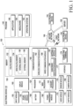
- FIG. 1 is a block diagram illustrating an electronic device 101 in a network environment 100 according to various embodiments.
- the electronic device 101 may include a processor 120, memory 130, an input module 150, a sound output module 155, a display module 160, an audio module 170, a sensor module 176, an interface 177, a connecting terminal
- the display module 160 may include a first display module 351 corresponding to the user's left eye and/or a second display module 353 corresponding to the user's right eye., a haptic module 179, a camera module 180, a power management module 188, a battery 189, a communication module 190, a subscriber identification module (SIM) 196, or an antenna module 197.
- SIM subscriber identification module
- At least one (e.g., the connecting terminal 178) of the components may be omitted from the electronic device 101, or one or more other components may be added in the electronic device 101.
- some (e.g., the sensor module 176, the camera module 180, or the antenna module 197) of the components may be integrated into a single component (e.g., the display module 160).
- the processor 120 may execute, for example, software (e.g., a program 140) to control at least one other component (e.g., a hardware or software component) of the electronic device 101 coupled with the processor 120, and may perform various data processing or computation.
- the processor 120 may store a command or data received from another component (e.g., the sensor module 176 or the communication module 190) in volatile memory 132, process the command or the data stored in the volatile memory 132, and store resulting data in non-volatile memory 134.
- the processor 120 may include a main processor 121 (e.g., a central processing unit (CPU) or an application processor (AP)), or an auxiliary processor 123 (e.g., a graphics processing unit (GPU), a neural processing unit (NPU), an image signal processor (ISP), a sensor hub processor, or a communication processor (CP)) that is operable independently from, or in conjunction with, the main processor 121.
- a main processor 121 e.g., a central processing unit (CPU) or an application processor (AP)
- auxiliary processor 123 e.g., a graphics processing unit (GPU), a neural processing unit (NPU), an image signal processor (ISP), a sensor hub processor, or a communication processor (CP)
- the main processor 121 may be configured to use lower power than the main processor 121 or to be specified for a designated function.
- the auxiliary processor 123 may be implemented as separate from, or as part of the main processor 121.
- the auxiliary processor 123 may control at least some of functions or states related to at least one component (e.g., the display module 160, the sensor module 176, or the communication module 190) among the components of the electronic device 101, instead of the main processor 121 while the main processor 121 is in an inactive (e.g., sleep) state, or together with the main processor 121 while the main processor 121 is in an active state (e.g., executing an application).
- the auxiliary processor 123 e.g., an image signal processor or a communication processor
- the auxiliary processor 123 may include a hardware structure specified for artificial intelligence model processing.
- the artificial intelligence model may be generated via machine learning. Such learning may be performed, e.g., by the electronic device 101 where the artificial intelligence is performed or via a separate server (e.g., the server 108). Learning algorithms may include, but are not limited to, e.g., supervised learning, unsupervised learning, semi-supervised learning, or reinforcement learning.
- the artificial intelligence model may include a plurality of artificial neural network layers.
- the artificial neural network may be a deep neural network (DNN), a convolutional neural network (CNN), a recurrent neural network (RNN), a restricted Boltzmann machine (RBM), a deep belief network (DBN), a bidirectional recurrent deep neural network (BRDNN), deep Q-network or a combination of two or more thereof but is not limited thereto.
- the artificial intelligence model may, additionally or alternatively, include a software structure other than the hardware structure.
- the memory 130 may store various data used by at least one component (e.g., the processor 120 or the sensor module 176) of the electronic device 101.
- the various data may include, for example, software (e.g., the program 140) and input data or output data for a command related thereto.
- the memory 130 may include the volatile memory 132 or the non-volatile memory 134.
- the program 140 may be stored in the memory 130 as software, and may include, for example, an operating system (OS) 142, middleware 144, or an application 146.
- OS operating system
- middleware middleware
- application application
- the input module 150 may receive a command or data to be used by other component (e.g., the processor 120) of the electronic device 101, from the outside (e.g., a user) of the electronic device 101.
- the input module 150 may include, for example, a microphone, a mouse, a keyboard, keys (e.g., buttons), or a digital pen (e.g., a stylus pen).
- the sound output module 155 may output sound signals to the outside of the electronic device 101.
- the sound output module 155 may include, for example, a speaker or a receiver.
- the speaker may be used for general purposes, such as playing multimedia or playing record.
- the receiver may be used for receiving incoming calls. According to an embodiment, the receiver may be implemented as separate from, or as part of the speaker.
- the display module 160 may visually provide information to the outside (e.g., a user) of the electronic device 101.
- the display 160 may include, for example, a display, a hologram device, or a projector and control circuitry to control a corresponding one of the display, hologram device, and projector.
- the display 160 may include a touch sensor configured to detect a touch, or a pressure sensor configured to measure the intensity of a force generated by the touch.
- the audio module 170 may convert a sound into an electrical signal and vice versa. According to an embodiment, the audio module 170 may obtain the sound via the input module 150, or output the sound via the sound output module 155 or a headphone of an external electronic device (e.g., an electronic device 102) directly (e.g., wiredly) or wirelessly coupled with the electronic device 101.
- an external electronic device e.g., an electronic device 102
- directly e.g., wiredly
- wirelessly e.g., wirelessly
- the sensor module 176 may detect an operational state (e.g., power or temperature) of the electronic device 101 or an environmental state (e.g., a state of a user) external to the electronic device 101, and then generate an electrical signal or data value corresponding to the detected state.
- the sensor module 176 may include, for example, a gesture sensor, a gyro sensor, an atmospheric pressure sensor, a magnetic sensor, an accelerometer, a grip sensor, a proximity sensor, a color sensor, an infrared (IR) sensor, a biometric sensor, a temperature sensor, a humidity sensor, or an illuminance sensor.
- the haptic module 179 may convert an electrical signal into a mechanical stimulus (e.g., a vibration or motion) or electrical stimulus which may be recognized by a user via his tactile sensation or kinesthetic sensation.
- the haptic module 179 may include, for example, a motor, a piezoelectric element, or an electric stimulator.
- the camera module 180 may capture a still image or moving images.
- the camera module 180 may include one or more lenses, image sensors, image signal processors, or flashes.
- the power management module 188 may manage power supplied to the electronic device 101.
- the power management module 188 may be implemented as at least part of, for example, a power management integrated circuit (PMIC).
- PMIC power management integrated circuit
- the battery 189 may supply power to at least one component of the electronic device 101.
- the battery 189 may include, for example, a primary cell which is not rechargeable, a secondary cell which is rechargeable, or a fuel cell.
- the communication module 190 may include a wireless communication module 192 (e.g., a cellular communication module, a short-range wireless communication module, or a global navigation satellite system (GNSS) communication module) or a wired communication module 194 (e.g., a local area network (LAN) communication module or a power line communication (PLC) module).
- a wireless communication module 192 e.g., a cellular communication module, a short-range wireless communication module, or a global navigation satellite system (GNSS) communication module
- GNSS global navigation satellite system
- wired communication module 194 e.g., a local area network (LAN) communication module or a power line communication (PLC) module.
- LAN local area network
- PLC power line communication
- the wireless communication module 192 may identify or authenticate the electronic device 101 in a communication network, such as the first network 198 or the second network 199, using subscriber information (e.g., international mobile subscriber identity (IMSI)) stored in the subscriber identification module 196.
- subscriber information e.g., international mobile subscriber identity (IMSI)
- the wireless communication module 192 may support a 5G network, after a 4G network, and next-generation communication technology, e.g., new radio (NR) access technology.
- the NR access technology may support enhanced mobile broadband (eMBB), massive machine type communications (mMTC), or ultra-reliable and low-latency communications (URLLC).
- eMBB enhanced mobile broadband
- mMTC massive machine type communications
- URLLC ultra-reliable and low-latency communications
- the wireless communication module 192 may support a high-frequency band (e.g., the mmWave band) to achieve, e.g., a high data transmission rate.
- the wireless communication module 192 may support various technologies for securing performance on a high-frequency band, such as, e.g., beamforming, massive multiple-input and multiple-output (massive MIMO), full dimensional MIMO (FD-MIMO), array antenna, analog beam-forming, or large scale antenna.
- the wireless communication module 192 may support various requirements specified in the electronic device 101, an external electronic device (e.g., the electronic device 104), or a network system (e.g., the second network 199).
- the wireless communication module 192 may support a peak data rate (e.g., 20Gbps or more) for implementing eMBB, loss coverage (e.g., 164dB or less) for implementing mMTC, or U-plane latency (e.g., 0.5ms or less for each of downlink (DL) and uplink (UL), or a round trip of 1ms or less) for implementing URLLC.
- a peak data rate e.g., 20Gbps or more
- loss coverage e.g., 164dB or less
- U-plane latency e.g., 0.5ms or less for each of downlink (DL) and uplink (UL), or a round trip of 1ms or less
- the antenna module 197 may transmit or receive a signal or power to or from the outside (e.g., the external electronic device).
- the antenna module 197 may include one antenna including a radiator formed of a conductor or conductive pattern formed on a substrate (e.g., a printed circuit board (PCB)).
- the antenna module 197 may include a plurality of antennas (e.g., an antenna array). In this case, at least one antenna appropriate for a communication scheme used in a communication network, such as the first network 198 or the second network 199, may be selected from the plurality of antennas by, e.g., the communication module 190.
- the signal or the power may then be transmitted or received between the communication module 190 and the external electronic device via the selected at least one antenna.
- other parts e.g., radio frequency integrated circuit (RFIC)
- RFIC radio frequency integrated circuit
- the antenna module 197 may form a mmWave antenna module.
- the mmWave antenna module may include a printed circuit board, a RFIC disposed on a first surface (e.g., the bottom surface) of the printed circuit board, or adjacent to the first surface and capable of supporting a designated high-frequency band (e.g., the mmWave band), and a plurality of antennas (e.g., array antennas) disposed on a second surface (e.g., the top or a side surface) of the printed circuit board, or adjacent to the second surface and capable of transmitting or receiving signals of the designated high-frequency band.
- a RFIC disposed on a first surface (e.g., the bottom surface) of the printed circuit board, or adjacent to the first surface and capable of supporting a designated high-frequency band (e.g., the mmWave band)
- a plurality of antennas e.g., array antennas
- At least some of the above-described components may be coupled mutually and communicate signals (e.g., commands or data) therebetween via an inter-peripheral communication scheme (e.g., a bus, general purpose input and output (GPIO), serial peripheral interface (SPI), or mobile industry processor interface (MIPI)).
- an inter-peripheral communication scheme e.g., a bus, general purpose input and output (GPIO), serial peripheral interface (SPI), or mobile industry processor interface (MIPI)
- commands or data may be transmitted or received between the electronic device 101 and the external electronic device 104 via the server 108 coupled with the second network 199.
- the external electronic devices 102 or 104 each may be a device of the same or a different type from the electronic device 101.
- all or some of operations to be executed at the electronic device 101 may be executed at one or more of the external electronic devices 102, 104, or 108. For example, if the electronic device 101 should perform a function or a service automatically, or in response to a request from a user or another device, the electronic device 101, instead of, or in addition to, executing the function or the service, may request the one or more external electronic devices to perform at least part of the function or the service.
- the one or more external electronic devices receiving the request may perform the at least part of the function or the service requested, or an additional function or an additional service related to the request, and transfer an outcome of the performing to the electronic device 101.
- the electronic device 101 may provide the outcome, with or without further processing of the outcome, as at least part of a reply to the request.
- a cloud computing, distributed computing, mobile edge computing (MEC), or client-server computing technology may be used, for example.
- the electronic device 101 may provide ultra low-latency services using, e.g., distributed computing or mobile edge computing.
- the external electronic device 104 may include an Internet-of-things (IoT) device.
- the server 108 may be an intelligent server using machine learning and/or a neural network.
- the external electronic device 104 or the server 108 may be included in the second network 199.
- the electronic device 101 may be applied to intelligent services (e.g., smart home, smart city, smart car, or health-care) based on 5G communication technology or IoT-related technology.
- the electronic device may be one of various types of electronic devices.
- the electronic devices may include, for example, a portable communication device (e.g., a smartphone), a computer device, a portable multimedia device, a portable medical device, a camera, a wearable device, or a home appliance.
- a portable communication device e.g., a smartphone
- a computer device e.g., a laptop, a desktop, a tablet, or a portable multimedia device
- a portable medical device e.g., a portable medical device
- camera e.g., a camera
- a wearable device e.g., a portable medical device
- each of such phrases as “A or B,” “at least one of A and B,” “at least one of A or B,” “A, B, or C,” “at least one of A, B, and C,” and “at least one of A, B, or C,” may include all possible combinations of the items enumerated together in a corresponding one of the phrases.
- such terms as “1st” and “2nd,” or “first” and “second” may be used to simply distinguish a corresponding component from another, and does not limit the components in other aspect (e.g., importance or order).
- an element e.g., a first element
- the element may be coupled with the other element directly (e.g., wiredly), wirelessly, or via a third element.
- module may include a unit implemented in hardware, software, or firmware, and may interchangeably be used with other terms, for example, “logic,” “logic block,” “part,” or “circuitry”.
- a module may be a single integral component, or a minimum unit or part thereof, adapted to perform one or more functions.
- the module may be implemented in a form of an application-specific integrated circuit (ASIC).
- ASIC application-specific integrated circuit
- Various embodiments as set forth herein may be implemented as software (e.g., the program 140) including one or more instructions that are stored in a storage medium (e.g., internal memory 136 or external memory 138) that is readable by a machine (e.g., the electronic device 101).
- a processor e.g., the processor 120
- the machine e.g., the electronic device 101
- the one or more instructions may include a code generated by a complier or a code executable by an interpreter.
- the storage medium readable by the machine may be provided in the form of a non-transitory storage medium.
- the term “non-transitory” simply means that the storage medium is a tangible device, and does not include a signal (e.g., an electromagnetic wave), but this term does not differentiate between where data is semi-permanently stored in the storage medium and where the data is temporarily stored in the storage medium.
- a method may be included and provided in a computer program product.
- the computer program products may be traded as commodities between sellers and buyers.
- the computer program product may be distributed in the form of a machine-readable storage medium (e.g., compact disc read only memory (CD-ROM)), or be distributed (e.g., downloaded or uploaded) online via an application store (e.g., Play Store TM ), or between two user devices (e.g., smart phones) directly. If distributed online, at least part of the computer program product may be temporarily generated or at least temporarily stored in the machine-readable storage medium, such as memory of the manufacturer's server, a server of the application store, or a relay server.
- CD-ROM compact disc read only memory
- an application store e.g., Play Store TM
- two user devices e.g., smart phones
- each component e.g., a module or a program of the above-described components may include a single entity or multiple entities. Some of the plurality of entities may be separately disposed in different components. According to various embodiments, one or more of the above-described components may be omitted, or one or more other components may be added. Alternatively or additionally, a plurality of components (e.g., modules or programs) may be integrated into a single component. In such a case, according to various embodiments, the integrated component may still perform one or more functions of each of the plurality of components in the same or similar manner as they are performed by a corresponding one of the plurality of components before the integration.
- operations performed by the module, the program, or another component may be carried out sequentially, in parallel, repeatedly, or heuristically, or one or more of the operations may be executed in a different order or omitted, or one or more other operations may be added.
- FIG. 2 is a view illustrating a state in which a second display area (e.g., the display area A2 of FIG. 3 ) of a display is received in a housing according to an embodiment of the disclosure.
- a second display area e.g., the display area A2 of FIG. 3
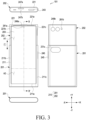
- FIG. 3 is a view illustrating a state in which a second display area of a display is exposed to the outside of a housing according to an embodiment of the disclosure.
- FIGS. 2 and 3 illustrate a structure in which the display 203 (e.g., flexible display or rollable display) is extended in the length direction (e.g., +Y direction) when the electronic device 101 is viewed from the front.
- the extending direction of the display 203 is not limited to one direction (e.g., +Y direction).
- the extending direction of the display 203 may be changed in design to be extendable in the upper direction (+Y direction), right direction (e.g., +X direction), left direction (e.g., -X direction), and/or lower direction (e.g., -Y direction).
- the state illustrated in FIG. 3 may be referred to as a slide-out state of the electronic device 101 or a state in which the second display area A2 of the display 203 is open.
- FIGS. 2 and 3 may be combined with the embodiment of FIG. 1 or the embodiments of FIGS. 4 to 14B .
- an electronic device 101 may include a housing 210.
- the housing 210 may include a first housing portion 201 and a second housing portion 202 disposed to be movable relative to the first housing portion 201.
- the electronic device 101 may be interpreted as having a structure in which the first housing portion 201 is disposed to be slidable with respect to the second housing portion 202.
- the second housing portion 202 may be disposed to perform reciprocating motion by a predetermined distance in a predetermined direction with respect to the first housing portion 201, for example, a direction indicated by an arrow 1.
- the first housing portion 201 may be referred to as a first housing 201.
- the second housing portion 202 may be referred to as a second housing 202.
- the second housing portion 202 may be referred to as a slide portion or a slide housing, and may be movable relative to the first housing portion 201.
- the second housing portion 202 may receive various electrical and electronic components, such as a circuit board or a battery.
- the second housing portion 202 When the electronic device 101 is in the slide-in state, the second housing portion 202 may be defined as being at a retracted position, and when the electronic device 101 is in the slide-out state, the second housing portion 202 may be defined as being at an extended position.
- the second housing portion 202 may be configured to move between the retracted position and the extended position with respect to the first housing portion 201.
- the slide-in state of the electronic device 101 may be changed into the slide-out state of the electronic device 101 (or the slide-in state of the electronic device 101) based on a predefined user input.
- the slide-in state of the electronic device 101 may be changed into the slide-out state (or the slide-in state of the electronic device 101) in response to a user input to a physical button exposed through a portion of the first housing portion 201 or a portion of the second housing portion 202.
- the slide-in state (or the slide-out state of the electronic device 101) may be changed into the slide-out state (or the slide-in state of the electronic device 101) in response to a touch input to an executable object displayed in the screen display area (e.g., the first display area A1).
- the slide-in state (or the slide-out state of the electronic device 101) may be changed into the slide-out state (or the slide-in state of the electronic device 101) in response to a touch input having a pressing strength of a reference strength or more at a contact point on the screen display area (e.g., the first display area A1).
- the slide-in state (or the slide-out state of the electronic device 101) may be changed into the slide-out state (or the slide-in state of the electronic device 101) in response to a voice input received through the microphone of the electronic device 101.
- the slide-in state (or the slide-out state of the electronic device 101) may be changed into the slide-out state (or the slide-in state of the electronic device 101) in response to an external force applied to the first housing portion 201 and/or the second housing portion 202 to move the second housing portion 202 with respect to the first housing portion 201.
- the slide-in state (or the slide-out state of the electronic device 101) may be changed into the slide-out state (or the slide-in state of the electronic device 101) in response to a user input identified from an external electronic device (e.g., earbuds or a smart watch) connected with the electronic device 101.
- an external electronic device e.g., earbuds or a smart watch
- the slide in-out operations of the electronic device 101 are not limited thereto.
- the first housing portion 201 may receive an actuator (e.g., a motor), a speaker, a sim socket, and/or a sub circuit board electrically connected with a main circuit board.
- the second housing portion 202 may receive a main circuit board on which electric components, such as an application processor (AP) or a communication processor (CP) are mounted.
- the second housing portion 202 may receive the actuator, speaker, sim socket, and/or the sub circuit board electrically connected with the main circuit board, and the first housing portion 201 may receive the main circuit board where electrical components, such as an application processor (AP) or a communication processor (CP), are mounted.
- the sub circuit board and the main circuit board may be disposed in the first housing portion 201 or the second housing portion 202.
- the first housing portion 201 may include a first cover member 211 (e.g., a main case).
- the first cover member 211 may include a 1-1th sidewall 211a, a 1-2th sidewall 211b extending from the 1-1th sidewall 211a, and a 1-3th sidewall 211c extending from the 1-1th sidewall 211a and substantially parallel to the 1-2th sidewall 211b.
- the 1-2th sidewall 211b and the 1-3th sidewall 211c may be formed substantially perpendicular to the 1-1th sidewall 211a.
- the 1-1th sidewall 211a, 1-2th sidewall 211b, and 1-3th sidewall 211c of the first cover member 211 may be formed to have an opening in a side surface (e.g., a front surface or front face) to receive (or surround) at least a portion of the second housing portion 202.
- a side surface e.g., a front surface or front face
- at least a portion of the second housing portion 202 may be surrounded by the first housing portion 201 and be slid in the direction parallel to the first surface (e.g., the first surface F1 of FIG. 4 ), e.g., arrow 1 direction, while being guided by the first housing portion 201.
- the 1-1th sidewall 211a, the 1-2th sidewall 211b, and/or the 1-3th sidewall 211c of the first cover member 211 may be integrally formed. According to an embodiment, the 1-1th sidewall 211a, the 1-2th sidewall 211b, and/or the 1-3th sidewall 211c of the first cover member 211 may be formed as separate structures and be combined or assembled.
- the first cover member 211 may be formed to surround at least a portion of the display 203.
- at least a portion of the display 203 may be formed to be surrounded by the 1-1th sidewall 211a, the 1-2th sidewall 211b, and/or the 1-3th sidewall 211c of the first cover member 211.
- the second housing portion 202 may include a second cover member 221 (e.g., a slide plate).
- the second cover member 221 may have a plate shape and include a first surface (e.g., the first surface F1 of FIG. 4 ) supporting internal components.
- the second cover member 221 may support at least a portion of the display 203 (e.g., the first display area A1).
- the second cover member 221 may be referred to as a front cover.
- the second cover member 221 may include a 2-1th sidewall 221a, a 2-2th sidewall 221b extending from the 2-1th sidewall 221a, and a 2-3th sidewall 221c extending from the 2-1th sidewall 221a and substantially parallel to the 2-2th sidewall 221b.
- the 2-2th sidewall 221b and the 2-3th sidewall 221c may be formed substantially perpendicular to the 2-1th sidewall 221a.
- the slide-in state and slide-out state of the electronic device 101 may be formed.
- the second housing portion 202 may be positioned at a first distance from the 1-1th sidewall 211a of the first housing portion 201.
- the second housing portion 202 may move to be positioned at a second distance larger than the first distance from the 1-1th sidewall 211a of the first housing portion 201.
- the first housing portion 201 may be formed to surround a portion of the 2-2th sidewall 221b and the 2-3th sidewall 221c.
- the area exposed to the outside may vary.
- the ratio of the width (e.g., length in the X direction) to the height (e.g., length in the Y direction) of the display 203 and/or the distance between the 1-1th sidewall 211a and the 2-1th sidewall 221a may be changed based on the slide of the electronic device 101.
- the electronic device 101 may include a display 203, a key input device 245, a connector hole 243, audio modules 247a and 247b, or camera modules 249a and 249b.
- the electronic device 101 may further include an indicator (e.g., a light emitting diode (LED) device) or various sensor modules.
- an indicator e.g., a light emitting diode (LED) device
- the display 203 may be formed so that the size of a portion of the housing 210, which may be viewed from the front, is changed based on the slide of the second housing portion 202.
- the display 203 may include a first display area A1 and a second display area A2 configured to be exposed to the outside of the electronic device 101 based on the slide of the second housing portion 202.
- the first display area A1 may be disposed on the second housing portion 202.
- the first display area A1 may be disposed on the second cover member 221 of the second housing portion 202.
- the second display area A2 may extend from the first display area A1, and the second display area A2 may be received in, or visually exposed to the outside of, the first housing portion 201 as the second housing portion 202 slides relative to the first housing portion 201.
- the display 203 may extend in the lower direction (e.g., -Y direction) of the electronic device 101.
- the second display area A2 may be visually exposed under the display 203 (e.g., in the -Y direction).
- the display 203 may extend in the upper direction (e.g., +Y direction) of the electronic device 101.
- the second display area A2 may be visually exposed above the display 203 (e.g., in the +Y direction).
- the second cover member 221 e.g., front cover
- the electronic device 101 changes from the slide-in state to slide-out state (e.g., if the second housing portion 202 slides to extend from the first housing portion 201)
- the second display area A2 may be gradually exposed to the outside of the first housing portion 201 and, together with the first display area A1, form a substantially flat surface.
- the display 203 may be coupled with or disposed adjacent to a touch detection circuit, a pressure sensor capable of measuring the strength (pressure) of touches, and/or a digitizer for detecting a magnetic field-type stylus pen.
- the exposed portion of the second display area A2 may be positioned on a portion (e.g., the curved surface 213a of FIG. 4 ) of the first housing portion, and a portion of the second display area A2 may remain in the curved shape in the position corresponding to the curved surface 213a.
- the key input device 245 may be positioned in an area of the housing 210 (e.g., the first housing portion 201 and/or second housing portion 202). Depending on the appearance and the state of use, the electronic device 101 may be designed to omit the illustrated key input device 245 or to include additional key input device(s). According to an embodiment, the electronic device 101 may include a key input device (not shown), e.g., a home key button or a touchpad disposed around the home key button. According to an embodiment, at least a portion of the key input device 245 may be disposed on the 1-1th sidewall 211a, the 1-2th sidewall 211b, or the 1-3th sidewall 211c of the first housing portion 201. According to an embodiment, at least a portion of the key input device 245 may be disposed on the 2-1th sidewall 221a, the 2-2th sidewall 221b, and/or the 2-3th sidewall 221c of the second housing portion 202.
- a key input device not shown
- the connector hole 243 may be omitted or may receive a connector (e.g., a universal serial bus (USB) connector) for transmitting and receiving power and/or data with an external electronic device.
- the electronic device 101 may include a plurality of connector holes 243, and some of the plurality of connector holes 243 may function as connector holes for transmitting/receiving audio signals with an external electronic device.
- the connector hole 243 is disposed in the second housing portion 202, but is not limited thereto.
- the connector hole 243 or a connector hole not shown may be disposed in the first housing portion 201.
- the audio modules 247a and 247b may include at least one speaker hole 247a or at least one microphone hole 247b.
- One of the speaker holes 247a may be provided as a receiver hole for voice calls, and the other may be provided as an external speaker hole.
- the electronic device 101 may include a microphone for obtaining sound. The microphone may obtain external sound of the electronic device 101 through the microphone hole 247b.
- the electronic device 101 may include a plurality of microphones to detect the direction of sound.
- the electronic device 101 may include an audio module in which the speaker hole 247a and the microphone hole 247b are implemented as one hole or may include a speaker without the speaker hole 247a (e.g., a piezo speaker).
- the speaker hole 247a and the microphone hole 247b may be positioned in the first housing portion 201 and/or the second housing portion 202.
- the first camera module 249a may be disposed to face in the same direction as the display 203.
- the first camera module 249a may be disposed in an area around the first display area A1 or overlapping the display 203.
- the first camera module 249a may capture the subject through the display 203.
- the first camera module 249a may include an under display camera (UDC) that has a screen display area (e.g., the first display area A1) that may not be visually exposed but hidden.
- the second camera module 249b may capture the subject in a direction opposite to the first display area A1.
- the first camera module 249a and/or the second camera module 249b may be disposed on the second housing portion 202.
- a plurality of second camera modules 249b may be formed to provide various arrays.
- the plurality of second camera modules 249b may be arranged along a width direction (X-axis direction) that is substantially perpendicular to the sliding direction (e.g., Y-axis direction) of the electronic device 101.
- the plurality of second camera modules 249b may be arranged along the sliding direction (e.g., Y-axis direction) of the electronic device 101.
- the plurality of second camera modules 249b may be arranged along N * M rows and columns like a matrix.
- the second camera module 249b is not visually exposed to the outside of the electronic device 101 in the slide-in state of the electronic device 101 and, in the slide-out state of the electronic device 101, may capture the outside of the electronic device 101.
- the second camera module 249b may capture the outside of the electronic device 101 in the slide-in state and/or slide-out state of the electronic device 101.
- at least a portion (e.g., the first rear plate 215 and/or the second rear plate 225 of FIG. 4 ) of the housing 210 may be substantially transparent.
- the second camera module 249b may capture the outside of the electronic device 101 through the first rear plate 215 and/or the second rear plate 225.
- the sensor modules 261a and 261b may include a first sensor module 261a (e.g., proximity sensor or illuminance sensor) disposed on the front surface of the electronic device 101 and/or a second sensor module 261b (e.g., heart rate monitoring (HRM) sensor) disposed on the rear surface of the electronic device 101.
- a first sensor module 261a e.g., proximity sensor or illuminance sensor
- a second sensor module 261b e.g., heart rate monitoring (HRM) sensor
- FIG. 5A is a cross-sectional view taken along line A-A' of FIG. 2 according to an embodiment of the disclosure.
- FIG. 5B is a cross-sectional view taken along line B-B' of FIG. 3 according to an embodiment of the disclosure.
- the first housing portion 201 may include a first cover member 211 (e.g., the first cover member 211 of FIGS. 2 and 3 ), a frame 213, and a first rear plate 215.
- a first cover member 211 e.g., the first cover member 211 of FIGS. 2 and 3
- a frame 213 e.g., the first rear plate 215.
- the first cover member 211 may receive at least a portion of the frame 213 and receive a component (e.g., battery 289) positioned in the frame 213.
- the first cover member 211 may be formed to surround at least a portion of the second housing portion 202.
- the first cover member 211 may protect the components (e.g., the second circuit board 249 and the frame 213) positioned in the first housing portion 201 from external impact.
- the second circuit board 249 electrically connected with an electric component e.g., an actuator, a speaker, a sim socket, and/or the first circuit board 248) may be connected to the first cover member 211.
- the first rear plate 215 may substantially form at least a portion of the exterior of the first housing portion 201 or the electronic device 101.
- the first rear plate 215 may be coupled to the outer surface of the first cover member 211.
- the first rear plate 215 may provide a decorative effect on the exterior of the electronic device 101.
- the first rear plate 215 may be formed of at least one of metal, glass, synthetic resin, or ceramic.
- the second cover member 221 may support at least a portion of the display 231.
- the second cover member 221 may include a first surface F1.
- the first display area A1 of the display 231 may be substantially positioned on the first surface F1 to maintain a flat panel shape.
- the second cover member 221 may be formed of a metal material and/or a non-metal (e.g., polymer) material.
- the first circuit board 248 receiving the electronic component e.g., the processor 120 and/or the memory 130 of FIG. 1
- the second cover member 221 may protect the components (e.g., the first circuit board 248 and the rear cover 223) positioned in the second housing portion 202 from external impact.
- the at least one antenna element 223a may include a laser direct structuring (LDS) antenna pattern formed on the outer surface of the rear cover 223.
- LDS laser direct structuring
- the at least one antenna element 223a may be formed to be embedded when the rear cover 223 is injection-molded.
- the at least one antenna element 223a may be configured to transmit or receive wireless signals in a designated frequency band (e.g., a legacy band) by electrically connecting with a wireless communication circuit (e.g., the wireless communication module 192 of FIG. 1 ) disposed on the first circuit board 248.
- a wireless communication circuit e.g., the wireless communication module 192 of FIG. 1
- the display assembly 230 may include a display 231 (e.g., the display 203 of FIGS. 2 and/or 3) and a multi-bar structure 232 supporting the display 231.
- the display 231 may be referred to as a flexible display, a foldable display, and/or a rollable display.
- the first display area A1 of the display 231 may be supported by a rigid body.
- the second display area A2 may be supported by a bendable structure.
- the first display area A1 may be supported by the first surface F1 of the second cover member 221 or a plate (not shown).
- the second display area A2 may be supported by the multi-bar structure 232.
- the driving structure 240 may move the second housing portion 202 relative to the first housing portion 201.
- the driving structure 240 may include an actuator 241 configured to generate a driving force for sliding the second housing portion 202 with respect to the first housing portion 201.
- the driving structure 240 may include a gear 244 (e.g., a pinion) connected to the actuator 241 and a rack 242 configured to mesh with the gear.
- FIG. 4 illustrates components (e.g., the actuator 241, the rack 242, and the gear 244) of the driving structure 240 inverted (e.g., facing in the -Z-axis direction) in the circle P1.
- the memory may include, e.g., a volatile or non-volatile memory.
- the interface may include, e.g., a high definition multimedia interface (HDMI), a universal serial bus (USB) interface, a secure digital (SD) card interface, and/or an audio interface.
- HDMI high definition multimedia interface
- USB universal serial bus
- SD secure digital
- the interface may electrically or physically connect, e.g., the electronic device 101 with an external electronic device and may include a USB connector, an SD card/multimedia card (MMC) connector, or an audio connector.
- MMC multimedia card
- the inner portion 252 of the guide rail 250 may provide a force to the multi-bar structure 232.
- the multi-bar structure 232 provided with the force may move along the slit 251 of the guide rail 250, and the second housing portion 202 may slide to extend with respect to the first housing portion 201.
- At least a portion of the display assembly 230 received between the first cover member 211 and the frame 213 may extend to the front surface.
- the second housing portion 202 may slide to be inserted into the first housing portion 201 through driving of the actuator 241.
- the gear 244 may rotate in a second rotation direction opposite to the first rotation direction based on the driving of the actuator 241.
- the second housing portion 202 may slide to enter the first housing portion 201 based on the sliding movement of the rack 242 toward the slide-in direction.
- the electronic device 101 may be configured to stop in a designated intermediate state between the slide-in state and the slide-out state by controlling driving of the actuator 241 (free stop function). According to an embodiment, the electronic device 101 may be changed to the slide-in state, the intermediate state, or the slide-out state through the user's manipulation in the state in which the driving force is not provided to the actuator 241.
- the configuration of the first housing portion 301 or the second housing portion 302 of FIGS. 6A and 6B may be identical in whole or part to the configuration of the first housing portion 201 or the second housing portion 202 of FIGS. 2 to 5B .
- the first housing portion 301 may include a first cover member 311 (e.g., the first cover member 211 of FIGS. 2 to 5B ).
- the second housing portion 302 may include a second cover member 321 (e.g., the second cover member 221 of FIGS. 2 to 5B ).
- the first housing portion 301 may be referred to as a first housing 301, and the second housing portion 302 may be referred to as a second housing 302.
- the first cover member 311 may include a first flat portion 311d, a 1-1th sidewall 311a (e.g., the 1-1th sidewall 211a of FIGS. 2 and 3 ), a 1-2th sidewall 311b (e.g., the 1-2th sidewall 211b of FIGS. 2 and 3 ), or a 1-3th sidewall 311c (e.g., the 1-3th sidewall 211c of FIGS. 2 and 3 ).
- a 1-1th sidewall 311a e.g., the 1-1th sidewall 211a of FIGS. 2 and 3
- a 1-2th sidewall 311b e.g., the 1-2th sidewall 211b of FIGS. 2 and 3
- a 1-3th sidewall 311c e.g., the 1-3th sidewall 211c of FIGS. 2 and 3
- the 1-3th sidewall 311c may be connected to the first flat portion 311d.
- the 1-3th sidewall 311c may be disposed perpendicular to the 1-1th sidewall 311a or may extend in a direction perpendicular to the 1-1th sidewall 311a.
- the 1-3th sidewall 311c may be disposed parallel to the 1-2th sidewall 311b.
- the second cover member 321 may include a second flat portion 321d, a 2-1th sidewall 321a (e.g., the 2-1th sidewall 221a of FIGS. 2 and 3 ), a 2-2th sidewall 321b (e.g., the 2-2th sidewall 221b of FIGS. 2 and 3 ), or a 2-3th sidewall 321c (e.g., the 2-3th sidewall 221c of FIGS. 2 and 3 ).
- the 2-3th sidewall 321c may be connected to the second flat portion 321d.
- the 2-3th sidewall 321c may be disposed perpendicular to the 2-1th sidewall 321a or may extend in a direction perpendicular to the 2-1th sidewall 321a.
- the 2-3th sidewall 321c may be disposed parallel to the 2-2th sidewall 321b.
- At least a portion of the first display area (e.g., the first display area A1 of FIG. 4 ) of the display may be disposed on or coupled to the other surface (e.g., the surface facing in the +Z direction of FIGS. 4 to 5B or the first surface F1 of FIG. 4 ) of the second flat portion 321d of the second cover member 321.
- the second cover member 321 may be configured to move between a retracted position (e.g., FIG. 2 , FIG. 5A , or FIG. 6A ) and an extended position (e.g.,
- the 2-2th sidewall 321b when the electronic device 101 is in the closed state (e.g., FIG. 2 , FIG. 5A , or FIG. 6A ), the 2-2th sidewall 321b may face the 1-2th sidewall 311b, and the 1-2th sidewall 311b may cover the 2-2th sidewall 321b.
- the 2-3th sidewall 321c When the electronic device 101 is in the closed state, the 2-3th sidewall 321c may face the 1-3th sidewall 311c, and the 1-3th sidewall 311c may cover the 2-3th sidewall 321c.
- At least a portion of the 2-2th sidewall 321b and/or at least a portion of the 2-3th sidewall 321c may be disposed to be exposed to the outside of the first housing portion 301 (or the first cover member 311).
- At least one of the 1-1th sidewall 311a, the 1-2th sidewall 311b, and the 1-3th sidewall 311c may include a first metallic area including a metallic material (e.g., aluminum or stainless steel) and a first non-metallic area including a non-metallic material (e.g., polymer).
- the first metallic area may be defined and/or denoted as a first conductive area including a conductive material.
- the first non-metallic area may be defined and/or denoted as a first non-conductive area including a non-conductive material.
- the first metallic area may form at least a portion of each of the 1-1th sidewall 311a, the 1-2th sidewall 311b, and/or the 1-3th sidewall 311c.
- the first non-metallic area may form the remaining portion of each of the 1-1th sidewall 311a, the 1-2th sidewall 311b, and/or the 1-3th sidewall 311c.
- the first metallic area may be defined as a frame forming at least a portion of the sidewalls 311a, 311b, and 311c of the first cover member 311, and the first non-metallic area may be defined as a segmentation portion forming the rest of the sidewalls 311a, 311b, and 311c.
- the segmentation portion may segment the frame into a plurality of metallic areas.
- the first antenna 312 may be electrically connected to at least a portion of the second housing portion 302 (or the second cover member 321) through the ground structure 330.
- the first antenna 312 may be electrically connected to the second metallic area of the second cover member 321 through the ground structure 330.
- the second metallic area of the second cover member 321 may provide a ground for the first antenna 312 through the ground structure 330.
- At least one of the 2-1th sidewall 321a, the 2-2th sidewall 321b, and the 2-3th sidewall 321c may include a second metallic area including a metallic material (e.g., aluminum or stainless steel) and a second non-metallic area including a non-metallic material (e.g., polymer).
- the second metallic area may be defined and/or denoted as a second conductive area including a conductive material.
- the second non-metallic area may be defined and/or denoted as a second non-conductive area including a non-conductive material.
- the second metallic area may form at least a portion of each of the 2-1th sidewall 321a, the 2-2th sidewall 321b, and/or the 2-3th sidewall 321c.
- the second non-metallic area may form the rest of each of the 2-1th sidewall 321a, the 2-2th sidewall 321b, and/or the 2-3th sidewall 321c.
- the second metallic area may be defined as a frame forming at least a portion of the sidewalls 321a, 321b, and 321c of the second cover member 321, and the second non-metallic area may be defined as a segmentation portion forming the rest of the sidewalls 321a, 321b, and 321c of the second cover member 321.
- the segmentation portion may segment the frame into a plurality of metallic areas.
- the second metallic area of the second cover member 321 may be electrically connected to a communication module (e.g., the communication module 190 of FIG. 1 ).
- the second metallic area of the second cover member 321 may be utilized as an antenna radiator (e.g., the antenna module 197 of FIG. 1 ) of the electronic device 101.
- the second antenna 322 may be defined and/or denoted as a second antenna radiator, a second antenna element, a second antenna module, or a second antenna device.
- the second antenna 322 may be electrically connected to the communication module.
- the electronic device 101 may be configured to transmit/receive signals to/from an external electronic device (e.g., the electronic devices 102 and 104 of FIG. 1 ) using the second antenna 322.
- the second antenna 322 may be electrically connected to at least a portion of the first housing portion 301 (or the first cover member 311) through the ground structure 330.
- the second antenna 322 may be electrically connected to the first metallic area of the first cover member 311 through the ground structure 330.
- the first metallic area of the first cover member 311 may provide a ground for the second antenna 322 through the ground structure 330.
- the electronic device 101 may further include a ground structure 330 that electrically connects the first metallic area of the first cover member 311 and the second metallic area of the second cover member 321.
- the ground structure 330 may radiate an antenna signal through an antenna radiator (e.g., the first antenna 311) formed in the first metallic area, thereby preventing the antenna performance of the electronic device 101 from deteriorating.
- an antenna radiator e.g., the first antenna 311
- the ground structure 330 may electrically connect the first antenna 312 provided by the first metallic area forming at least a portion of the sidewalls 311a, 311b, and 311c of the first cover member 311 and the second antenna 322 provided by the second metallic area forming at least a portion of the sidewalls 321a, 321b, and 321c of the second cover member 321.
- a signal fed to the second antenna 322 of the second cover member 321 through a circuit board e.g., the first circuit board 248 of FIG.
- the ground structure 330 may electrically connect the second antenna 322 of the second cover member 321 and the first metallic area of the first cover member 311.
- the second antenna 322 may receive a ground from the first metallic area of the first cover member 311 through the ground structure 330 in the open state of the electronic device 101. Accordingly, in the open state of the electronic device 101, the performance degradation of the second antenna 322 may be limited or reduced.
- the first antenna 312 may remain electrically connected to the second antenna 322 (or the second metallic area) through the ground structure 330.
- FIG. 7 may be combined with the embodiments of FIGS. 1 to 6B or the embodiments of FIGS. 8 to 14B .
- an electronic device 101 may include a first cover member 311 or a ground structure 330.
- the configuration of the first cover member 311 or the ground structure 330 of FIG. 7 may be identical in whole or part to the configuration of the first cover member 311 or the ground structure 330 of FIGS. 6A and 6B .
- the first cover member 311 may include a 1-2th sidewall 311b (e.g., the 1-2th sidewall 311b of FIGS. 6A and 6B ).
- the ground structure 330 may be formed of a conductive material or a metallic material.
- the ground structure 330 may be referred to as a linear guide (e.g., the linear guide 400 of FIG. 8 ).
- the ground structure 330 may include a first guide portion 331, a second guide portion (e.g., the second guide portion 420 of FIG. 8 ), or a conductive contact portion 333.
- the conductive contact portion 333 may protrude from the second guide portion.
- the conductive contact portion 333 may include a coupling portion 3331 coupled to the second guide portion.
- the conductive contact portion 333 may include a first contact portion 3332 or a second contact portion 3333.
- the first contact portion 3332 may protrude from the coupling portion 3331 toward the 1-2th sidewall 311b of the first cover member 311.
- the first contact portion 3332 may extend to be inclined with respect to the coupling portion 3331.
- the first cover member 311 and/or the 1-2th sidewall 311b may include an accommodation space 313.
- the accommodation space 313 may provide a space in which the conductive contact portion 333 is movable.
- the accommodation space 313 may be formed on an inner surface (e.g., a surface facing in the +X direction of FIGS. 6B to 8 ) of the 1-2th sidewall 311b facing the 2-2th sidewall (e.g., the 2-2th sidewall 321b of FIG. 6B or the 2-2th sidewall 321b of FIG. 8 ).
- the accommodation space 313 may be defined and/or denoted as a recess or groove recessed in the inner surface of the 1-2th sidewall 311b.
- the accommodation space 313 may include an extended area 3131, a first inclined area 3132, or a second inclined area 3133.
- the extended area 3131 may be disposed between the first inclined area 3132 and the second inclined area 3133.
- the extended area 3131 may be parallel to the moving direction (e.g., the Y-axis direction of FIGS. 7 to 8 ) of the second housing portion (e.g., the second housing portion 302 of FIG. 8 ).
- the extended area 3131 may be substantially parallel to the extending direction (e.g., the Y-axis direction of FIGS. 7 to 8 ) of the 1-2th sidewall 311b.
- the extended area 3131 like the first inclined area 3132 and/or the second inclined area 3133, may be inclined with respect to the moving direction (e.g., the Y-axis direction of FIGS. 7 to 8 ) of the second housing portion.
- the extended area 3131 may include a partial area at least partially inclined with respect to the moving direction of the second housing portion.
- the first inclined area 3132 may be inclined with respect to the moving direction of the second housing portion.
- the first inclined area 3132 may be inclined with respect to the extended area 3131.
- the first inclined area 3132 may contact the first contact portion 3332 when the state of the electronic device 101 is the closed state (e.g., FIG. 2 , FIG. 5A , or FIG. 6A ).
- the first inclined area 3132 may be electrically connected to the first contact portion 3332 through the first metal sheet 3352 in the closed state of the electronic device 101.
- the second inclined area 3133 may be inclined with respect to the moving direction of the second housing portion.
- the second inclined area 3133 may be inclined with respect to the extended area 3131.
- the second inclined area 3133 may contact the second contact portion 3333 when the state of the electronic device 101 is the open state (e.g., FIG. 3 , FIG. 5B , or FIG. 6B ).
- the second inclined area 3133 may be electrically connected to the second contact portion 3333 through the second metal sheet 3353 in the closed state of the electronic device 101.
- the conductive contact portion 333 may be configured to be electrically connected to the inclined areas 3132 and 3133 when the second housing portion is located at a retracted position or an extended position.
- the conductive contact portion 333 may be configured to be electrically connected to the first inclined area 3132 when the second housing portion is located at the retracted position (e.g., FIG. 2 , FIG. 5A , or FIG. 6A ).
- the conductive contact portion 333 may be configured to be electrically connected to the second inclined area 3133 when the second housing portion is located at an extended position (e.g., FIG. 3 , FIG. 5B , or FIG. 6B ).
- the ground structure 330 may electrically connect the first metallic area (or first conductive area) of the first cover member 311 and the second metallic area (or second conductive area) of the second cover member (e.g., the second cover member 321 of FIG. 6B or the second cover member 321 of FIG. 8 ).
- the first contact portion 3332 may contact the first metal sheet 3352.
- the first metallic area (or the first conductive area) of the first cover member 311 may be electrically connected to the second metallic area (or the second conductive area) of the second cover member (e.g., the second cover member 321 of FIG. 6B or the second cover member 321 of FIG. 8 ) through the first inclined area 3132, the first metal sheet 3352, the first contact portion 3332, the coupling portion 3331, the first guide portion 331, and the second guide portion (e.g., the second guide portion 420 of FIG. 8 ).
- the second contact portion 3333 may contact the second metal sheet 3353.
- the first metallic area (or the second conductive area) of the first cover member 311 may be electrically connected to the second metallic area (or the second conductive area) of the second cover member (e.g., the second cover member 321 of FIG. 6B or the second cover member 321 of FIG. 8 ) through the second inclined area 3133, the second metal sheet 3353, the second contact portion 3333, the coupling portion 3331, the first guide portion 331, and the second guide portion (e.g., the second guide portion 420 of FIG. 8 ).
- the first contact portion 3332 and/or the second contact portion 3333 may not contact the extended area 3131 but may be spaced apart from the extended area 3131. Accordingly, when the second housing portion (e.g., the second housing portion 302 of FIG. 8 ) moves, as the conductive contact portion 333 is spaced apart from the extended area 3131, the occurrence of scratches in the extended area 3131 may be limited or reduced. Further, damage to the conductive contact portion 333 may be limited or reduced.
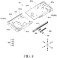
- FIG. 8 is a perspective view illustrating an electronic device according to an embodiment of the disclosure.
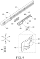
- FIG. 9 is an exploded perspective view illustrating a linear guide according to an embodiment of the disclosure.
- FIG. 10A is a side view illustrating an electronic device in a closed state thereof according to an embodiment of the disclosure.
- FIG. 10A is a side view illustrating an electronic device in an open state thereof according to an embodiment of the disclosure.
- FIGS. 8 to 10B may be combined with the embodiments of FIGS. 1 to 7 , or the embodiments of FIGS. 11 to 12B .
- an electronic device 101 may include a first housing portion 301, a second housing portion 302, or a linear guide 400.
- the configuration of the first housing portion 301 or the second housing portion 302 of FIGS. 8 to 10B may be identical in whole or part to the configuration of the first housing portion 301 or the second housing portion 302 of FIGS. 6A and 6B .
- the configuration of the linear guide 400 of FIGS. 8 to 10B may be identical in whole or part to the configuration of the ground structure 330 of FIGS. 6A to 7 .
- the first housing portion 301 may include a first cover member 311 (e.g., the first cover member 311 of FIGS. 6A and 6B ).
- the first cover member 311 may include a 1-1th sidewall 311a (e.g., the 1-1th sidewall 311a of FIGS. 6A and 6B ), a 1-2th sidewall 311b (e.g., the 1-2th sidewall 311b of FIGS. 6A and 6B ), a 1-3th sidewall 311c (e.g., the 1-3th sidewall 311c of FIGS. 6A and 6B ), or a first flat portion 311d (e.g., the first flat portion 311d of FIGS. 6A and 6B ).
- the first housing portion 301 may be referred to as a first housing 301.
- the second housing portion 302 may include a second cover member 321 (e.g., the second cover member 321 of FIG. 6B ).
- the second cover member 321 may include a 2-1th sidewall 321a (e.g., the 2-1th sidewall 321a of FIG. 6B ), a 2-2th sidewall 321b (e.g., the 2-2th sidewall 321b of FIG. 6B ), a 2-3th sidewall 321c (e.g., the 2-3th sidewall 321c of FIG. 6B ), or a second flat portion 321d (e.g., the second flat portion 321d of FIG. 6B ).
- the second housing portion 302 may be referred to as a second housing 302.
- the first housing portion 301 may include an accommodation space 313 (e.g., the accommodation space 313 of FIG. 7 ).
- the accommodation space 313 may be formed in each of the 1-2th sidewall 311b and the 1-3th sidewall 311c.
- the accommodation space 313 formed in the 1-2th sidewall 311b is described as an example, but the description thereof may be equally applied and/or understood for the accommodation space formed in the 1-3th sidewall 311c.
- the accommodation space 313 may be recessed in a portion of the first side surface 311b or 311c that faces the second side surface 321b or 321c.
- the electronic device 101 may further include a linear guide 400.
- a linear guide 400 may be provided.
- One of the pair of linear guides 400 may be disposed between the 1-2th sidewall 311b and the 2-2th sidewall 321b, and the other one of the pair of linear guides 400 may be disposed between the 1-3th sidewall 311c and the 2-3th sidewall 321c.
- the linear guide 400 disposed between the 1-3th sidewall 311c and the 2-3th sidewall 321c is described as an example, but the description thereof may be equally applied and/or understood for the linear guide disposed between the 1-2th sidewall 311b and the 2-2th sidewall 321b.
- the 1-2th sidewall 311b and/or the 1-3th sidewall 311c of the first cover member 311 on which the linear guide 400 is disposed may be defined and/or denoted as the first side surface 311b or 311c of the first housing 301.
- the 2-2th sidewall 321b or 321c of the second cover member 321 on which the linear guide 400 is disposed may be defined and/or denoted as the second side surface 321b or 321c of the second housing 302.
- the first housing portion 301 may include first side surfaces 311b and 311c or a first antenna (e.g., the first antenna 312 of FIGS. 6A and 6B ).
- the second housing portion 302 may include second side surfaces 321b and 321c or a second antenna (e.g., the second antenna 322 of FIG. 6B ).
- the second side surfaces 321b and 321c may face the first side surfaces 311b and 311c.
- the linear guide 400 may be configured to stably guide the sliding movement of the second housing portion 302.
- the linear guide 400 may restrict or reduce the movement or shaking of the second housing portion 302 relative to the first housing portion 301 in the front direction (e.g., the +Z direction of FIG. 8 ) and/or the rear direction (e.g., the -Z direction of FIG. 8 ) of the electronic device 101.
- the linear guide 400 may stably guide the sliding movement of the second housing portion 302 in a linear direction.
- the linear guide 400 may include a first guide portion 410 (e.g., the first guide portion 331 of FIG. 7 ), a second guide portion 420, a conductive contact portion 430 (e.g., the conductive contact portion 333 of FIG. 7 ), or a bearing 440.
- the first guide portion 410 may be disposed on the 1-3th sidewall 311c.
- the first guide portion 410 may be coupled to or fixed to an inner surface (e.g., a surface facing the -X direction of FIG. 8 ) of the 1-3th sidewall 311c facing the 2-3th sidewall 321c.
- the second guide portion 420 may be slidably coupled to the first guide portion 410.
- the first guide portion 410 may include a first body portion 411, a rail 412, a first coupling hole 413, or a damper 414.
- the first body portion 411 may be coupled to the 1-3th sidewall 311c.
- the first body portion 411 may be fixed to the 1-3th sidewall 311c through a fastening member (e.g., a bolt or pin) disposed in the first coupling hole 413 formed through the first body portion 411.
- the first body portion 411 may be formed of a metallic material.
- the rail 412 may be recessed from at least a portion of the first body portion 411.
- the second body portion 421 of the second guide portion 420 may be inserted into the rail 412.
- the rail 412 may extend in a sliding direction (e.g., the Y-axis direction of FIG. 8 ) of the second housing portion 302.
- the second body portion 422 of the second guide portion 420 may slide on the rail 412.
- the damper 414 may be disposed on the rail 412.
- the damper 414 may be coupled to one end (e.g., an end facing in the -Y direction of FIG. 9 ) of the second body portion 421 of the second guide portion 420.
- the damper 414 may be formed of an elastically deformable material (e.g., rubber). The damper 414 may reduce or restrict excessive impact from being transferred to one end of the second body portion 421 when the second guide portion 420 slides.
- the second guide portion 420 may include a second body portion 421, a recess 422, a second coupling hole 423, or a seat portion 424.
- the second body portion 421 may be coupled to the 2-3th sidewall 321c.
- the second body portion 421 may be fixed to the 2-3th sidewall 321c through a fastening member (e.g., a bolt or pin) disposed in the second coupling hole 423 formed through the second body portion 421.
- the second body portion 421 may be formed of a metallic material.
- the recess 422 may be formed at each of an upper end (e.g., an end facing in the +Z direction of FIG. 9 ) and a lower end (e.g., an end facing in the -Z direction of FIG. 9 ) of the second body portion 421.
- the recess 422 may be recessed from at least a portion of the second body portion 421.
- the bearing 440 may be disposed between the recess 422 and the rail 412.
- the bearing 440 may include a ball bearing configured to reduce a frictional force generated between the second guide portion 420 and the first guide portion 410 when the second guide portion 420 moves with respect to the first guide portion 410.
- the seat portion 424 may be recessed in one surface of the second body portion 421 that faces the 1-3th sidewall 311c.
- the seat portion 424 may be defined as a recess or groove for receiving the conductive contact portion 430.
- the conductive contact portion 430 may be formed of a metallic material.
- the conductive contact portion 430 may include a coupling portion 431 coupled to or accommodated in the seat portion 424.
- the conductive contact portion 430 may include a first contact portion 432 (e.g., the first contact portion 3332 of FIG. 7 ) protruding or extending from the coupling portion 431 (e.g., the coupling portion 3331 of FIG. 7 ), and/or a second contact portion 433 (e.g., the second contact portion 3333 of FIG. 7 ).
- the second guide portion 420 may move together with the second housing portion 302 as the second housing portion 302 moves. Further, as the second guide portion 420 moves, the conductive contact portion 430 may move together with the second guide portion 420 and/or the second housing portion 302.
- the first contact portion 432 may contact a first metal sheet (e.g., the first metal sheet 314a of FIG. 11 ).
- the second contact portion 433 may contact a second metal sheet (e.g., the second metal sheet 314b of FIG. 11 ) when the state of the electronic device 101 is the open state (e.g., FIG. 10B ).
- the first contact portion 432 and/or the second contact portion 433 may have a shape of a c-clip, but is not limited thereto. According to an embodiment, the first contact portion 432 and the second contact portion 433 may be disposed to cross each other. According to an embodiment (not shown), the first contact portion 432 and the second contact portion 433 may be defined by a portion of a dome structure.
- the conductive contact portion 430 may be formed to have the shape of a dome structure
- the first contact portion 432 may include an inclined surface defined by a partial area of the dome structure
- the second contact portion 433 may include an inclined surface defined by an area different from the partial area of the dome structure.
- FIG. 11 is a perspective view illustrating a first housing portion including a receiving space according to an embodiment of the disclosure.
- FIG. 12A is a cross-sectional view illustrating a first inclined area according to an embodiment of the disclosure.
- FIG. 12B is a cross-sectional view illustrating a second inclined area according to an embodiment of the disclosure.
- FIG. 13A is a cross-sectional view illustrating a linear guide in a closed state of an electronic device according to an embodiment of the disclosure.
- FIG. 13B is a cross-sectional view illustrating a linear guide in an open state of an electronic device according to an embodiment of the disclosure.
- FIG. 14B is a view illustrating a conductive contact portion in an open state of an electronic device according to an embodiment of the disclosure.
- FIGS. 11 to 14B may be combined with the embodiments of FIGS. 1 to 10B .
- the configuration of the first housing portion 301 or the linear guide 400 of FIGS. 11 to 14B may be identical in whole or part to the configuration of the first housing portion 301 or the linear guide 400 of FIGS. 8 to 10B .
- the at least one metal sheet 314 may include a first metal sheet 314a or a second metal sheet 314b.
- the 1-1th inclined area 3132a may be inclined with respect to the sliding direction (e.g., the Y-axis direction of FIGS. 8 to 12B ) of the second housing portion (e.g., the second housing portion 302 of FIGS. 8 to 10B ).
- the inclination angle d1 between the 1-1th inclination area 3132a and the sliding direction may be about 13 to 17 degrees.
- the inclination angle d1 may be about 15 degrees.
- the 2-1th inclined area 3133a may be inclined with respect to the sliding direction (e.g., the Y-axis direction of FIGS. 8 to 12B ) of the second housing portion (e.g., the second housing portion 302 of FIGS. 8 to 10B ).
- the inclination angle d2 between the 2-1th inclination area 3133a and the sliding direction may be about 13 to 17 degrees.
- the inclination angle d2 may be about 15 degrees.
- the conductive contact portion 430 may include a coupling portion 431 (e.g., the coupling portion 431 of FIG. 9 ), a first contact portion 432 (e.g., the first contact portion 432 of FIG. 9 ), or a second contact portion 433 (e.g., the second contact portion 433 of FIG. 9 ).
- the conductive contact portion 430 may be configured to be electrically connected to the inclined areas 3132 and 3133 when the second housing portion 302 is located at a retracted position or an extended position.
- the conductive contact portion 430 may be configured to be electrically connected to the first inclined area 3132 when the second housing portion 302 is located at the retracted position (e.g., FIG. 2 , FIG. 5A , FIG. 6A , FIG. 10A , FIG. 13A , or FIG. 14A ).
- the conductive contact portion 430 may be configured to be electrically connected to the second inclined area 3133 when the second housing portion 302 is located at an extended position (e.g., FIG. 3 , FIG. 5B , FIG. 6B , FIG. 10B , FIG. 13B , or FIG. 14B ).
- FIGS. 13A and 14A are cross-sectional views illustrating a linear guide 400 when the electronic device 101 is in a closed state (e.g., FIG. 2 , FIG. 5A , FIG. 6A , or FIG. 10A ).
- the first contact portion 432 when the electronic device 101 is in the closed state, the first contact portion 432 (e.g., the first contact portion 432 of FIG. 9 ) may contact the first metal sheet 314a. As the first contact portion 432 contacts the first metal sheet 314a, the conductive contact portion 430 may be electrically connected to the 1-1th inclined area 314a through the first metal sheet 314a.
- the depth t1 (e.g., the depth in the X-axis direction of FIG. 13A ) of the seat portion 424 (e.g., the seat portion 424 of FIG. 9 ) may be about 0.2 mm to about 0.4 mm.
- the depth t1 may be about 0.3 mm.
- the coupling portion 431 of the conductive contact portion 430 may be disposed or accommodated in the seat portion 424 of the second guide portion 420.
- a gap t2 (e.g., the gap t2 of FIG. 13A ) formed between the second guide portion 420 and the 1-2th sidewall 311b may be about 0.2 mm to about 0.4 mm.
- the gap t2 may be about 0.3 mm.
- first metal sheet 314a may be spaced apart from the seat portion 424 by a second vertical distance h2 (e.g., the distance in the X-axis direction in FIG. 13A ) larger than the first vertical distance h1.
- the first vertical distance h1 may be about 0.5 mm to about 0.7 mm
- the second vertical distance h2 may be about 0.9 mm to about 1.1 mm.
- the first vertical distance h1 may be about 0.6 mm
- the second vertical distance h2 may be about 1.0 mm.
- the first contact portion 432 may smoothly contact the first metal sheet 314a.
- the first contact portion 432 may contact the first metal sheet 314a and may be at least partially elastically deformed.
- the first contact portion 432 may not be stuck to the first metal sheet 314a. Accordingly, an electrical connection structure between the first contact portion 432 and the first metal sheet 314a may be stably provided.
- the second contact portion 433 when the electronic device 101 is in the open state, the second contact portion 433 (e.g., the second contact portion 433 of FIG. 9 ) may contact the second metal sheet 314b. As the second contact portion 433 contacts the second metal sheet 314b, the conductive contact portion 430 may be electrically connected to the 2-1th inclined area 314b through the second metal sheet 314b.
- the first vertical distance h1 may be about 0.5 mm to about 0.7 mm
- the second vertical distance h2 may be about 0.9 mm to about 1.1 mm
- the first vertical distance h1 may be about 0.6 mm
- the second vertical distance h2 may be about 1.0 mm.
- the second contact portion 433 may smoothly contact the second metal sheet 314b.
- the second housing portion 302 moves in the slide-out direction (e.g., the +Y direction of FIG. 13B )
- the second contact portion 433 may contact the second metal sheet 314b and may be at least partially elastically deformed.
- the second contact portion 433 may not be stuck to the second metal sheet 314b, and thus an electrical connection structure between the second contact portion 433 and the second metal sheet 314b may be stably provided.
- an antenna structure or an antenna radiator may be formed or disposed in each of the first housing and the second housing. Since at least one of the antenna structure or the antenna radiator formed in each of the first housing and the second housing is disposed adjacent to another antenna structure or antenna radiator, it may be difficult to sufficiently secure antenna performance.
- the first side surface 311b or 311c may include an accommodation space 313.
- the accommodation space 313 may be recessed in a portion of the first side surface 311b or 311c that faces the second side surface 321b or 321c.
- the accommodation space 313 may include the inclined area 3132 or 3133 or an extended area 3131.
- the extended area 3131 may extend from the inclined area 3132 or 3133.
- the extended area 3131 may be spaced apart from the conductive contact portion 430.
- the inclined area 3132 or 3233 may include a first inclined area 3132 or a second inclined area 3133.
- the first inclined area 3132 may be configured to be electrically connected to the conductive contact portion 430 when the second housing 202 or 302 is located at the retracted position.
- the second inclined area 3133 may be configured to be electrically connected to the conductive contact portion 430 when the second housing 202 or 302 are located at the extended position.
- the extended area 3131 may extend parallel to a moving direction of the second housing 202 or 302.
- the first inclined area 3132 may be connected to one end of the extended area 3131.
- the second inclined area 3133 may be connected to another end of the extended area 3131.
- a direction in which the first inclined area 3132 is inclined with respect to the extended area 3131 may be different from a direction in which the second inclined area 3133 is inclined with respect to the extended area 3131.
- the second guide portion 420 may include a second body portion 421 or a seat portion 424.
- the second body portion 421 may be coupled to the second side surface 321b or 321c.
- the second body portion 421 may be movably coupled to the rail 412.
- the seat portion 424 may be recessed from at least a portion of the second body portion 421.
- the conductive contact portion 430 may be disposed on the seat portion 424.
- the conductive contact portion 430 may include a coupling portion 431, a first contact portion 432, or a second contact portion 433.
- the coupling portion 431 may be coupled to the seat portion 424.
- the first contact portion 432 may protrude from the coupling portion 431.
- the second contact portion 433 may protrude from the coupling portion 432.
- the second contact portion 433 may be spaced apart from the first contact portion 432.
- the linear guide 400 includes a first guide portion 410, a second guide portion 420, or a conductive contact portion 430.
- the first guide portion 410 is coupled to the first side surface 311b or 311c.
- the second guide portion 420 is coupled to the second side surface 321b or 321c.
- the second guide portion 420 is movable relative to the first guide portion 410.
- the conductive contact portion 430 protrudes from the second guide portion 420.
- the first side surface 311b or 311c includes an inclined area 3132 or 3133.
- the inclined area 3132 or 3133 is inclined with respect to a moving direction of the second housing 202 or 302.
- the conductive contact portion 430 is configured to be electrically connected to the inclined area 3132 or 3133 when the second housing 202 or 302 is located at the retracted position or the extended position.
- the linear guide 400 may further include a bearing 440.
- the bearing 440 may be disposed between the first guide portion 410 and the second guide portion 420.
- the second guide portion 420 may include a second body portion 421 or a seat portion 424.
- the second body portion 421 may be coupled to the second side surface 321b or 321c.
- the second body portion 421 may be movably coupled to the rail 412.
- the seat portion 424 may be recessed from at least a portion of the second body portion 421.
- the conductive contact portion 430 may be disposed on the seat portion 424.
Landscapes
- Engineering & Computer Science (AREA)
- Computer Networks & Wireless Communication (AREA)
- Signal Processing (AREA)
- Telephone Set Structure (AREA)
Applications Claiming Priority (3)
| Application Number | Priority Date | Filing Date | Title |
|---|---|---|---|
| KR20230108977 | 2023-08-21 | ||
| KR1020230115553A KR20250028155A (ko) | 2023-08-21 | 2023-08-31 | 안테나 구조 및 이를 포함하는 전자 장치 |
| PCT/KR2024/011674 WO2025042094A1 (ko) | 2023-08-21 | 2024-08-07 | 안테나 구조 및 이를 포함하는 전자 장치 |
Publications (2)
| Publication Number | Publication Date |
|---|---|
| EP4535560A1 true EP4535560A1 (de) | 2025-04-09 |
| EP4535560A4 EP4535560A4 (de) | 2025-08-20 |
Family
ID=92494396
Family Applications (1)
| Application Number | Title | Priority Date | Filing Date |
|---|---|---|---|
| EP24751968.9A Pending EP4535560A4 (de) | 2023-08-21 | 2024-08-07 | Antennenstruktur und elektronische vorrichtung damit |
Country Status (3)
| Country | Link |
|---|---|
| EP (1) | EP4535560A4 (de) |
| CN (1) | CN121713331A (de) |
| WO (1) | WO2025042094A1 (de) |
Family Cites Families (6)
| Publication number | Priority date | Publication date | Assignee | Title |
|---|---|---|---|---|
| US12284307B2 (en) * | 2020-01-09 | 2025-04-22 | Lg Electronics Inc. | Mobile terminal |
| KR20220027600A (ko) * | 2020-08-27 | 2022-03-08 | 삼성전자주식회사 | 안테나 및 이를 구비한 전자 장치 |
| KR102290231B1 (ko) * | 2020-09-28 | 2021-08-20 | 삼성전자주식회사 | 플렉서블 디스플레이를 포함하는 전자 장치 |
| EP4136705A4 (de) * | 2020-10-12 | 2023-10-25 | Samsung Electronics Co., Ltd. | Elektronische vorrichtung mit antenne |
| KR102950194B1 (ko) * | 2020-11-16 | 2026-04-08 | 삼성전자주식회사 | 안테나를 포함하는 전자 장치 |
| KR20230071672A (ko) * | 2021-11-16 | 2023-05-23 | 삼성전자주식회사 | 접지 구조를 포함하는 전자 장치 |
-
2024
- 2024-08-07 WO PCT/KR2024/011674 patent/WO2025042094A1/ko active Pending
- 2024-08-07 CN CN202480053004.8A patent/CN121713331A/zh active Pending
- 2024-08-07 EP EP24751968.9A patent/EP4535560A4/de active Pending
Also Published As
| Publication number | Publication date |
|---|---|
| WO2025042094A1 (ko) | 2025-02-27 |
| CN121713331A (zh) | 2026-03-20 |
| EP4535560A4 (de) | 2025-08-20 |
Similar Documents
| Publication | Publication Date | Title |
|---|---|---|
| EP4492190A1 (de) | Aufrollbare elektronische vorrichtung mit mehrstangenstruktur | |
| US20230195167A1 (en) | Heat dissipation structure and electronic device including the same | |
| US20250140496A1 (en) | Rollable electronic device comprising button structure | |
| US20250030789A1 (en) | Driving structure and electronic device comprising same | |
| KR20230143905A (ko) | 구동 구조 및 이를 포함하는 전자 장치 | |
| EP4535560A1 (de) | Antennenstruktur und elektronische vorrichtung damit | |
| EP4492568A1 (de) | Antennenstruktur und elektronische vorrichtung damit | |
| EP4274024A1 (de) | Antennenstruktur und elektronische vorrichtung damit | |
| US20250016940A1 (en) | Antenna structure and electronic device including same | |
| EP4542975B1 (de) | Antriebsstruktur und elektronische vorrichtung damit | |
| EP4738049A1 (de) | Transparentes fenster und elektronische vorrichtung damit | |
| US20240431048A1 (en) | Rollable electronic device comprising guide assembly | |
| EP4722853A1 (de) | Führungsstruktur und elektronische vorrichtung damit | |
| EP4645287A1 (de) | Rollbare anzeige und elektronische vorrichtung damit | |
| EP4498662B1 (de) | Elektronische vorrichtung mit drahtloser ladefunktion und betriebsverfahren dafür | |
| US20260051649A1 (en) | Electronic device comprising flexible display | |
| EP4529367A1 (de) | Elektronische vorrichtung mit flexibler leiterplatte | |
| EP4723604A1 (de) | Elektronische vorrichtung mit antriebsanordnung | |
| US20250318060A1 (en) | Electronic device for controlling driving module on basis of detection of fall, and control method therefor | |
| EP4730071A1 (de) | Flexible anzeige und elektronische vorrichtung damit | |
| US12603413B2 (en) | Electronic apparatus including antenna | |
| EP4622231A1 (de) | Rollbare elektronische vorrichtung mit messschaltung | |
| US12596406B2 (en) | Electronic device comprising driving element | |
| US12439535B2 (en) | Electronic device including elastic member | |
| KR20250028155A (ko) | 안테나 구조 및 이를 포함하는 전자 장치 |
Legal Events
| Date | Code | Title | Description |
|---|---|---|---|
| STAA | Information on the status of an ep patent application or granted ep patent |
Free format text: STATUS: UNKNOWN |
|
| STAA | Information on the status of an ep patent application or granted ep patent |
Free format text: STATUS: THE INTERNATIONAL PUBLICATION HAS BEEN MADE |
|
| PUAI | Public reference made under article 153(3) epc to a published international application that has entered the european phase |
Free format text: ORIGINAL CODE: 0009012 |
|
| STAA | Information on the status of an ep patent application or granted ep patent |
Free format text: STATUS: REQUEST FOR EXAMINATION WAS MADE |
|
| 17P | Request for examination filed |
Effective date: 20240815 |
|
| AK | Designated contracting states |
Kind code of ref document: A1 Designated state(s): AL AT BE BG CH CY CZ DE DK EE ES FI FR GB GR HR HU IE IS IT LI LT LU LV MC ME MK MT NL NO PL PT RO RS SE SI SK SM TR |
|
| A4 | Supplementary search report drawn up and despatched |
Effective date: 20250717 |
|
| RIC1 | Information provided on ipc code assigned before grant |
Ipc: H01Q 1/24 20060101AFI20250711BHEP Ipc: H04M 1/02 20060101ALI20250711BHEP Ipc: H01Q 1/48 20060101ALI20250711BHEP |
|
| GRAP | Despatch of communication of intention to grant a patent |
Free format text: ORIGINAL CODE: EPIDOSNIGR1 |
|
| STAA | Information on the status of an ep patent application or granted ep patent |
Free format text: STATUS: GRANT OF PATENT IS INTENDED |
|
| RIC1 | Information provided on ipc code assigned before grant |
Ipc: H01Q 1/24 20060101AFI20251128BHEP Ipc: H04M 1/02 20060101ALI20251128BHEP Ipc: H01Q 21/28 20060101ALI20251128BHEP Ipc: H01Q 9/04 20060101ALI20251128BHEP |
|
| DAV | Request for validation of the european patent (deleted) | ||
| DAX | Request for extension of the european patent (deleted) | ||
| INTG | Intention to grant announced |
Effective date: 20260102 |
|
| RIN1 | Information on inventor provided before grant (corrected) |
Inventor name: KIM, HYUNSUK Inventor name: KANG, JOOYOUNG Inventor name: KIM, YOUNGCHUL Inventor name: PARK, HONGBUM Inventor name: YUN, INKUK Inventor name: LEE, SOYOUNG Inventor name: LEE, WONHO Inventor name: JANG, SEOKMIN |
|
| GRAS | Grant fee paid |
Free format text: ORIGINAL CODE: EPIDOSNIGR3 |
|
| GRAA | (expected) grant |
Free format text: ORIGINAL CODE: 0009210 |
|
| STAA | Information on the status of an ep patent application or granted ep patent |
Free format text: STATUS: THE PATENT HAS BEEN GRANTED |