EP4535635A1 - Stromwandler und verfahren zum betrieb eines stromwandlers - Google Patents
Stromwandler und verfahren zum betrieb eines stromwandlers Download PDFInfo
- Publication number
- EP4535635A1 EP4535635A1 EP23202168.3A EP23202168A EP4535635A1 EP 4535635 A1 EP4535635 A1 EP 4535635A1 EP 23202168 A EP23202168 A EP 23202168A EP 4535635 A1 EP4535635 A1 EP 4535635A1
- Authority
- EP
- European Patent Office
- Prior art keywords
- power converter
- switch
- coupled
- capacitor
- terminal
- Prior art date
- Legal status (The legal status is an assumption and is not a legal conclusion. Google has not performed a legal analysis and makes no representation as to the accuracy of the status listed.)
- Pending
Links
Images


Classifications
-
- H—ELECTRICITY
- H02—GENERATION; CONVERSION OR DISTRIBUTION OF ELECTRIC POWER
- H02M—APPARATUS FOR CONVERSION BETWEEN AC AND AC, BETWEEN AC AND DC, OR BETWEEN DC AND DC, AND FOR USE WITH MAINS OR SIMILAR POWER SUPPLY SYSTEMS; CONVERSION OF DC OR AC INPUT POWER INTO SURGE OUTPUT POWER; CONTROL OR REGULATION THEREOF
- H02M1/00—Details of apparatus for conversion
- H02M1/42—Circuits or arrangements for compensating for or adjusting power factor in converters or inverters
- H02M1/4208—Arrangements for improving power factor of AC input
-
- H—ELECTRICITY
- H02—GENERATION; CONVERSION OR DISTRIBUTION OF ELECTRIC POWER
- H02M—APPARATUS FOR CONVERSION BETWEEN AC AND AC, BETWEEN AC AND DC, OR BETWEEN DC AND DC, AND FOR USE WITH MAINS OR SIMILAR POWER SUPPLY SYSTEMS; CONVERSION OF DC OR AC INPUT POWER INTO SURGE OUTPUT POWER; CONTROL OR REGULATION THEREOF
- H02M7/00—Conversion of AC power input into DC power output; Conversion of DC power input into AC power output
- H02M7/02—Conversion of AC power input into DC power output without possibility of reversal
- H02M7/04—Conversion of AC power input into DC power output without possibility of reversal by static converters
- H02M7/12—Conversion of AC power input into DC power output without possibility of reversal by static converters using discharge tubes with control electrode or semiconductor devices with control electrode
- H02M7/21—Conversion of AC power input into DC power output without possibility of reversal by static converters using discharge tubes with control electrode or semiconductor devices with control electrode using devices of a triode or transistor type requiring continuous application of a control signal
- H02M7/217—Conversion of AC power input into DC power output without possibility of reversal by static converters using discharge tubes with control electrode or semiconductor devices with control electrode using devices of a triode or transistor type requiring continuous application of a control signal using semiconductor devices only
-
- H—ELECTRICITY
- H02—GENERATION; CONVERSION OR DISTRIBUTION OF ELECTRIC POWER
- H02M—APPARATUS FOR CONVERSION BETWEEN AC AND AC, BETWEEN AC AND DC, OR BETWEEN DC AND DC, AND FOR USE WITH MAINS OR SIMILAR POWER SUPPLY SYSTEMS; CONVERSION OF DC OR AC INPUT POWER INTO SURGE OUTPUT POWER; CONTROL OR REGULATION THEREOF
- H02M3/00—Conversion of DC power input into DC power output
- H02M3/02—Conversion of DC power input into DC power output without intermediate conversion into AC
- H02M3/04—Conversion of DC power input into DC power output without intermediate conversion into AC by static converters
- H02M3/10—Conversion of DC power input into DC power output without intermediate conversion into AC by static converters using discharge tubes with control electrode or semiconductor devices with control electrode
- H02M3/145—Conversion of DC power input into DC power output without intermediate conversion into AC by static converters using discharge tubes with control electrode or semiconductor devices with control electrode using devices of a triode or transistor type requiring continuous application of a control signal
- H02M3/155—Conversion of DC power input into DC power output without intermediate conversion into AC by static converters using discharge tubes with control electrode or semiconductor devices with control electrode using devices of a triode or transistor type requiring continuous application of a control signal using semiconductor devices only
- H02M3/156—Conversion of DC power input into DC power output without intermediate conversion into AC by static converters using discharge tubes with control electrode or semiconductor devices with control electrode using devices of a triode or transistor type requiring continuous application of a control signal using semiconductor devices only with automatic control of output voltage or current, e.g. switching regulators
- H02M3/158—Conversion of DC power input into DC power output without intermediate conversion into AC by static converters using discharge tubes with control electrode or semiconductor devices with control electrode using devices of a triode or transistor type requiring continuous application of a control signal using semiconductor devices only with automatic control of output voltage or current, e.g. switching regulators including plural semiconductor devices as final control devices for a single load
- H02M3/1582—Buck-boost converters
Definitions
- the present application relates to power converters and to methods of operating power converters.
- Power converters are generally used to convert an input electrical power to an output electrical power.
- a mains AC (alternating current) voltage e.g., 110 V or 220 V, depending on the country, may be converted to a DC (direct current) voltage of 5 V, 12 V, 24 V or any other voltage required for a particular application.
- DC (direct current) voltage e.g., 5 V, 12 V, 24 V or any other voltage required for a particular application.
- Various kinds of power converters are conventionally known, like buck converters, boost converters, buck-boost converters, flyback converters, etc.
- more than one power converter stage is used in a power converter.
- a first stage may be used for so called power factor correction, which reduces losses due to the real power not matching the apparent power in the system.
- This first stage converts the input AC power to an intermediate DC voltage, also referred to as bus voltage.
- a first stage for example buck converters, boost converters or buck-boost converters may be used.
- a second stage for example a flyback converter, then converts the bus voltage to the desired output voltage.
- a power converter as defined in claim 1 and a method as defined in claim 11 are provided.
- the dependent claims define further embodiments.
- a corresponding controller as defined in claim 12, a system as defined in claim 13 and a computer program as defined in claim 14 are also provided.
- a power converter comprising:
- a method of operating a power converter as mentioned above comprising:
- connections or couplings shown in the drawings or described herein refer to electrical connections or couplings unless noted otherwise. Such connections or couplings are to be understood in a functional way, i.e., to provide a certain function within the circuits discussed herein. The connections or couplings may be modified for example by adding or removing elements, as long as the respective function of the connection or coupling is preserved.
- Embodiments discussed herein use diode components.
- a diode component, as used herein, is a component that is or includes a diode.
- a diode component may be a PN diode, a PIN diode, a transistor coupled as a diode, a transistor having a body diode (which is then the diode of the diode component), and which may remain in a switched off state such that only the diode is operative, etc.
- Switches as used herein may be implemented as transistor switches.
- switches may be implemented as bidirectional switches.
- a bidirectional switch when switched off, does not conduct current in either direction.
- Bidirectional switches may be implemented using gallium nitride (GaN) transistors, where body diodes, if present, have a high forward voltage and therefore in the voltage range the transistor is intended for does not conduct current, or may be switched off for both current directions by applying a negative gate voltage.
- GaN gallium nitride
- MOSFET transistors per se usually do not qualify as bidirectional switches because of their body diode.
- a bidirectional switch may be constructed based on two MOSFET transistors in series with opposite orientations of source and drain.
- Other transistor types than field effect transistors may also be used, like bipolar junction transistors (BJTs) or insulated gate bipolar transistors (IGBTs), such that showing and describing specific transistor types herein is not to be construed as limiting.
- a switch is referred to as off or opened when it is essentially non-conducting between its terminals, and as on or closed if it conducts current between its terminals.
- Embodiments herein relate to a new topology of power converters which essentially may act as buck-boost converters, i.e., converting an input voltage to a higher or lower output voltage.
- Such converters as described herein may be used as standalone power converters, but may also be used as a stage of a multistage power converter, for example a power factor correction stage.
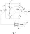
- Fig. 1 is a circuit diagram of a power converter according to an embodiment.
- the power converter of Fig. 1 comprises a first input node 10 and a second input node 11.
- An AC input voltage, symbolized by a current source AC, in operation is coupled between first input node 10 and second input node 11.
- a current supplied to the power converter in operation is labelled Iin in Fig. 1 , and a corresponding input voltage Vin.
- a first diode D 1 is coupled between first input node 10 and intermediate node 12, and a second diode D 2 is coupled between second input node 11 and intermediate node 12.
- the polarities of diodes D 1 and D 2 are opposite each other, such that for both diodes, the anode sides are coupled to the respective first or second input terminal 10, 11 and both cathode sides are coupled to intermediate node 12.
- An inductor L1 is coupled between first intermediate node 12 and a second intermediate node 13.
- a first terminal of inductor L1 is coupled to first intermediate node 12, and a second terminal of inductor L1 is coupled to a second intermediate node 13.
- a first switch S 4 is coupled between first input terminal 10 and second intermediate node 13, and a second switch S 3 is coupled between second input terminal 11 and second intermediate node 13.
- Switches S 4 , S 3 may be bidirectional switches, for example GaN (Gallium Nitride) based switches.
- a diode D 3 is coupled between second intermediate node 13 and a first terminal of an output capacitor C1, with an anode side towards second intermediate node 13 and a cathode side towards a first terminal of capacitor C1.
- the first terminal of inductor L1 and a second terminal of capacitor C1 are coupled to ground as shown. In Fig. 1 they are coupled with each other and then to ground, but in other embodiments they may be connected to (the same) ground separately. Instead of ground, another reference potential may also be used.
- An output current Iout is supplied by an output voltage Vout across capacitor C1 as shown.
- the arrows at Iin, Iout and Vout denote the positive direction of the corresponding current or voltage used in signal graphs in the following.
- inductor L1 and capacitor C1 may be selected based on an intended operation range of the power converter.
- ranges e.g. input voltage range, output voltage range etc.
- mean values, maximum values typical values or values resulting in maximum loading of the inductor L of the ranges may be used for selecting L.
- controller 15 Operation of the power converter of Fig. 1 may be controlled by controller 15.
- controller is not to be construed as limiting and refers to any entity which is capable of controlling the power converter for the functions explained below, and may for example include a microprocessor programmed accordingly, an application specific integrated circuit (ASIC), gate drivers for driving switches S 3 and S 4 etc.
- ASIC application specific integrated circuit
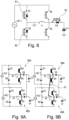
- the negative charging phase is shown in Fig. 2C , when the input voltage is negative.
- Fig. 2C by applying corresponding gate source voltages to switches S 3 and S 4 , first switch S 4 is on, and second switch S 3 is off.
Landscapes
- Engineering & Computer Science (AREA)
- Power Engineering (AREA)
- Rectifiers (AREA)
Priority Applications (1)
| Application Number | Priority Date | Filing Date | Title |
|---|---|---|---|
| EP23202168.3A EP4535635A1 (de) | 2023-10-06 | 2023-10-06 | Stromwandler und verfahren zum betrieb eines stromwandlers |
Applications Claiming Priority (1)
| Application Number | Priority Date | Filing Date | Title |
|---|---|---|---|
| EP23202168.3A EP4535635A1 (de) | 2023-10-06 | 2023-10-06 | Stromwandler und verfahren zum betrieb eines stromwandlers |
Publications (1)
| Publication Number | Publication Date |
|---|---|
| EP4535635A1 true EP4535635A1 (de) | 2025-04-09 |
Family
ID=88295797
Family Applications (1)
| Application Number | Title | Priority Date | Filing Date |
|---|---|---|---|
| EP23202168.3A Pending EP4535635A1 (de) | 2023-10-06 | 2023-10-06 | Stromwandler und verfahren zum betrieb eines stromwandlers |
Country Status (1)
| Country | Link |
|---|---|
| EP (1) | EP4535635A1 (de) |
Citations (1)
| Publication number | Priority date | Publication date | Assignee | Title |
|---|---|---|---|---|
| US8233298B2 (en) * | 2008-06-05 | 2012-07-31 | Delta Electronics, Inc. | Power factor correction rectifier that operates efficiently over a range of input voltage conditions |
-
2023
- 2023-10-06 EP EP23202168.3A patent/EP4535635A1/de active Pending
Patent Citations (1)
| Publication number | Priority date | Publication date | Assignee | Title |
|---|---|---|---|---|
| US8233298B2 (en) * | 2008-06-05 | 2012-07-31 | Delta Electronics, Inc. | Power factor correction rectifier that operates efficiently over a range of input voltage conditions |
Non-Patent Citations (3)
| Title |
|---|
| BANAGAR MARUTHI ET AL: "Design and simulation of bridgeless PFC buck boost converter fed BLDC motor drive", 2017 INNOVATIONS IN POWER AND ADVANCED COMPUTING TECHNOLOGIES (I-PACT), IEEE, 21 April 2017 (2017-04-21), pages 1 - 7, XP033287574, DOI: 10.1109/IPACT.2017.8244880 * |
| HOU XIAOHAN ET AL: "A Novel Lower Inductance Quasi-bridgeless Active Power Factor Corrector", 2019 14TH IEEE CONFERENCE ON INDUSTRIAL ELECTRONICS AND APPLICATIONS (ICIEA), IEEE, 19 June 2019 (2019-06-19), pages 1307 - 1312, XP033616251, DOI: 10.1109/ICIEA.2019.8833951 * |
| ZHAO BEN ET AL: "Family of Bridgeless Buck-Boost PFC Rectifiers", IEEE TRANSACTIONS ON POWER ELECTRONICS, INSTITUTE OF ELECTRICAL AND ELECTRONICS ENGINEERS, USA, vol. 30, no. 12, 1 December 2015 (2015-12-01), pages 6524 - 6527, XP011667353, ISSN: 0885-8993, [retrieved on 20150824], DOI: 10.1109/TPEL.2015.2445779 * |
Similar Documents
| Publication | Publication Date | Title |
|---|---|---|
| US10651731B1 (en) | Zero voltage switching of interleaved switched-capacitor converters | |
| US10727747B2 (en) | Hybrid buck-boost converter | |
| US10833594B2 (en) | System and method of controlling a power converter having an LC tank coupled between a switching network and a transformer winding | |
| US6310785B1 (en) | Zero voltage switching DC-DC converter | |
| US8233298B2 (en) | Power factor correction rectifier that operates efficiently over a range of input voltage conditions | |
| US10819222B2 (en) | Circuitry for power factor correction and methods of operation | |
| EP1331723A2 (de) | Mehrphasige Gleichstrom/Gleichstrom-Spannungsversorgung mit niedriger Ausgangsspannung, starkem Strom, Halbbrücke und Reihenresonanz | |
| EP3267568A1 (de) | Stromwandler | |
| EP3553928B1 (de) | Entstörerschaltung und ein dieses verwendende leistungsumwandlungssystem | |
| WO2012001828A1 (ja) | Dc/dc電力変換装置 | |
| US10361624B2 (en) | Multi-cell power converter with improved start-up routine | |
| US10193464B2 (en) | DC-DC converter | |
| US11296607B2 (en) | DC-DC converter | |
| CN115868105A (zh) | 软开关脉冲宽度调制dc-dc功率转换器 | |
| CN103731047A (zh) | 电源设备 | |
| US10097106B1 (en) | Power converter | |
| CN108475991B (zh) | 隔离式直流-直流变换器及其电压变换方法 | |
| KR20190115364A (ko) | 단상 및 3상 겸용 충전기 | |
| EP1763124A2 (de) | Gleichstromwandler | |
| US11705809B2 (en) | Voltage converter | |
| EP4535635A1 (de) | Stromwandler und verfahren zum betrieb eines stromwandlers | |
| CN107005174B (zh) | 隔离直流/直流转换器及电压转换方法 | |
| CN102710131A (zh) | 变换器及其驱动方法及包含该变换器的功率因数校正装置 | |
| Jiang et al. | A single-stage 6.78 MHz transmitter with the improved light load efficiency for wireless power transfer applications | |
| EP2680418A2 (de) | Resonanzwandler mit Common-Core zur Leistungsfaktorkorrektur |
Legal Events
| Date | Code | Title | Description |
|---|---|---|---|
| PUAI | Public reference made under article 153(3) epc to a published international application that has entered the european phase |
Free format text: ORIGINAL CODE: 0009012 |
|
| STAA | Information on the status of an ep patent application or granted ep patent |
Free format text: STATUS: THE APPLICATION HAS BEEN PUBLISHED |
|
| AK | Designated contracting states |
Kind code of ref document: A1 Designated state(s): AL AT BE BG CH CY CZ DE DK EE ES FI FR GB GR HR HU IE IS IT LI LT LU LV MC ME MK MT NL NO PL PT RO RS SE SI SK SM TR |
|
| STAA | Information on the status of an ep patent application or granted ep patent |
Free format text: STATUS: REQUEST FOR EXAMINATION WAS MADE |
|
| 17P | Request for examination filed |
Effective date: 20251008 |